Article

Light Confinement in Twisted Single-Layer 2D+ Moiré Photonic Crystals and Bilayer Moiré Photonic Crystals

1
Department of Physics, University of North Texas, Denton, TX 76203, USA
2
Department of Materials Science and Engineering, University of North Texas, Denton, TX 76203, USA
3
Department of Electrical Engineering, University of North Texas, Denton, TX 76203, USA
*
Author to whom correspondence should be addressed.
Photonics 2024, 11(1), 13; https://doi.org/10.3390/photonics11010013
Submission received: 6 November 2023 / Revised: 21 December 2023 / Accepted: 23 December 2023 / Published: 25 December 2023
(This article belongs to the Special Issue Recent Advances in Micro-Nano Optics)

Abstract

:
Twisted photonic crystals are photonic analogs of twisted monolayer materials such as graphene and their optical property studies are still in their infancy. This paper reports optical properties of twisted single-layer 2D+ moiré photonic crystals where there is a weak modulation in z direction, and bilayer moiré-overlapping-moiré photonic crystals. In weak-coupling bilayer moiré-overlapping-moiré photonic crystals, the light source is less localized with an increasing twist angle, similar to the results reported by the Harvard research group in References 37 and 38 on twisted bilayer photonic crystals, although there is a gradient pattern in the former case. In a strong-coupling case, however, the light source is tightly localized in AA-stacked region in bilayer PhCs with a large twist angle. For single-layer 2D+ moiré photonic crystals, the light source in Ex polarization can be localized and forms resonance modes when the single-layer 2D+ moiré photonic crystal is integrated on a glass substrate. This study leads to a potential application of 2D+ moiré photonic crystal in future on-chip optoelectronic integration.

1. Introduction

Recent studies of twisted moiré graphene (twistronics) have resulted in numerous exotic phenomena including magic-angle physics and magic-angle flat-band superconductivity [1,2,3,4,5,6]. This explosion of magic-angle physics has advanced from bilayer moiré graphene [7,8] to twisted bilayers of two-dimensional (2D) transition metal dichalcogenide materials [9,10,11,12], to the recent mixing of moiré surface and bulk states in graphite [13] and moiré quasicrystals [6]. With increasing moiré periods in length scale, the twistronics for electrons has been advanced to twisted metasurfaces [14,15,16] and twisted photonic crystals (PhCs) (twistoptics for photons) [17,18]. There are also flat-band modes and magic angles in twisted bilayer PhCs through the mode coupling between two twisted layers [19,20,21,22,23,24,25]. Moiré flat-band thresholdless lasing [22] in twistoptics is the optical analogy to superconductivity in twistronics.
Moiré PhCs can be twisted bilayers [8,18,20,21,23,24,26,27,28,29,30,31,32,33,34,35,36,37,38] that can be ideally fabricated by E-beam lithography or a twisted single-layer moiré pattern [19,22,39,40,41,42,43,44,45,46,47,48], which is formed by laser interference in photorefractive crystals, holographic lithography, or E-beam lithography. The single-layer moiré photonic lattice has been generated in a photorefractive crystal by a shallow modulation of the refractive index induced by two mutually twisted laser interferences. However, both sublattices interfere in one plane [39,40,45]. When four laser beams are arranged in a cone geometry and form an interference pattern, a conventional PhC can be obtained through holographic lithography. When eight laser beams are separated into two sets with each arranged in different cone angles (where one cone angle is much larger than the other) in holographic interference geometry, twisted moiré PhCs can be fabricated holographically [49,50,51]. By including a central laser beam with eight laser beams in cone arrangement, three-dimensional (3D) moiré PhCs have been fabricated [52,53].
These single-layer moiré PhCs can be easily fabricated by holographic fabrication while the fabrication of bilayer PhCs is rather complicated. Resonance modes have been observed in twisted single-layer moiré PhCs covering Mie resonances, photonic band edge resonances, and resonance modes above the light line that might be topological bound states in continuum (BIC), assuming a 2D pattern [17]. Actually, the interference pattern formed by eight beams in two-cone geometry is not 2D because there is a weak modulation in z direction. Here, we name them as twisted 2D+ moiré PhCs. It is interesting to know whether the light can be confined in these 2D+ moiré PhCs. In this paper, light confinement is studied in two types of twisted PhCs: moiré PhCs superposed against each other with a relative rotation angle (moiré-overlapping-moiré) and single-layer 2D+ moiré PhCs. We initially repeat our simulations and compare them with the Harvard research group results in References 37 and 38. Then, we study the light confinement in 2D+ moiré silicon PhCs with a certain thickness, and thereafter the case where the 2D+ moiré silicon PhCs is on a glass substrate.

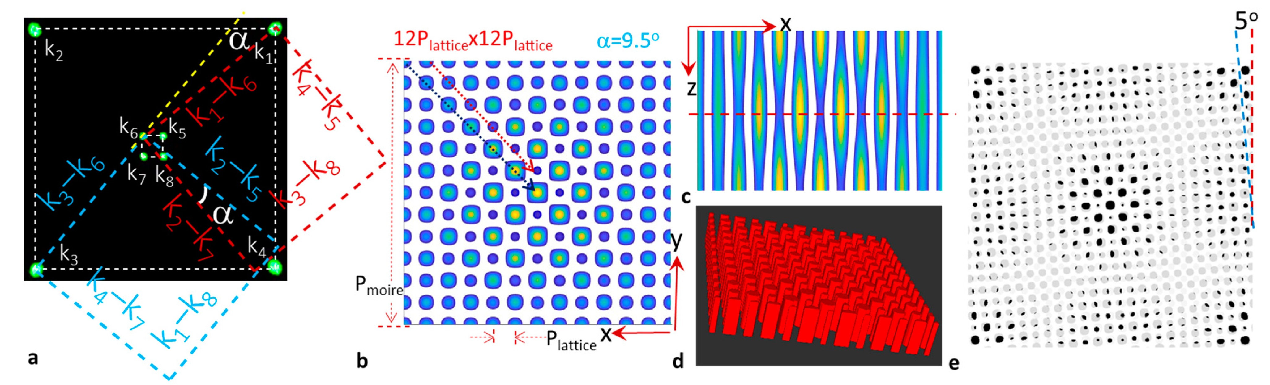
2. Concepts and Simulation Methods

The orientation of the interference pattern of two laser beams with wavevectors of kn and km is determined by the wave vector difference km-kn. Two sets of laser beams are shown in Figure 1a in the Fourier filter of 4f imaging system as green spots. The wavevectors in the xy plane of four outer beams are labeled as k1, k2, k3, and k4, while the xy components of four inner beams are k5, k6, k7, and k8. As shown in Figure 1a, the wave vector difference (k3-k6) is rotated from (k1-k6) by an angle of α. The blue dashed square formed by (k3-k6), (k4-k7), (k1-k8), and (k2-k5) is rotated from the red dashed square of (k3-k8), (k4-k5), (k1-k6), and (k2-k7) by an angle of α, as well. When all eight beams are overlapped, a moiré interference pattern can be formed as seen in Figure 1b, where the moiré period Pmoiré and lattice period Plattice are indicated. The moiré interference intensity of these eight beams, I (x,y,z), can be calculated by Equation (1):
I   x , y , z = i = 1 8 E i 2 ( x , y , z , t ) + i < j 8 E i E j e i · e j c o s k j k i · r + ( δ j δ i )
where e is the polarization of the electric field, k is the wave vector of laser beams, E is the electric field, and δ is the initial phase. These four outer beams, k1, k2, k3, and k4, determine the lattice constant Plattice. When the interference angles among the four inner beams, k5, k6, k7, and k8, are much smaller than those of the four outer beams, then k5, k6, k7, and k8 determine the moiré lattice constant Pmoire. Thus, the relationship between Pmoiré and Plattice with the twist angle α can be approximately calculated by Equation (2) [17]:
P m o i r e P l a t t i c e tan α 2
For the interference pattern in xy plane in Figure 1b with a unit super-cell size of 12plattice × 12plattice, the twist angle is calculated to be 9.5 degrees using Equation (2). There are two sublattices as indicated by the blue dashed arrow for motif size increase and red dashed arrow for motif size decrease. The interference pattern in the xz plane is shown in Figure 1c with one z period. There is a modulation in z direction, however, the modulation is gradient. It is stronger in the central region than at the edge in Figure 1c. The weak coupling between dual sublattices lead to a disappearance of the first-order diffraction spots of (1, 0), (0, 1), (−1, 0), and (0, −1) as confirmed by the experiments [48].
Here, we generate two types of patterns. One type is for conventional twisted PhCs where there is no z-direction modulation in the top or bottom layer PhC separated by a spacer in order to compare our results with the Harvard research group [37,38]. However, we add a moiré pattern in the top or bottom layer that is different from the Harvard research group. There are many parameters of top (bottom) layer thickness, spacer thickness, rotation angle, and material permittivity that can modify the light confinement. We start with parameters of top (bottom) layer thickness, spacer thickness, and rotation angles from the Harvard research group in References 37 and 38, then further evaluate the light confinement related to the thickness and material permittivity. The second type of pattern maintains the z-direction modulation in Figure 1c.
We describe the generation of the first type of pattern below. For moiré PhC rotating by an angle of α and overlaying on another moiré PhC, we calculate the interference intensity for the xy plane in z location as indicated by the red dashed line in Figure 1c using a Python program. When the intensity of interference = I (x,y,0) is larger than the threshold intensity Ith which is 18% of maximum of I (x,y,z) (Imax), we assign a refractive index n = 3.48; otherwise, n = 1 (air). In the Python program, a certain thickness of pattern was obtained by filling it with the pattern I (x,y,0) as shown in Figure 1d, an output image of the Python simulation. However, for the pattern in Figure 1e, we assign n = 1 if I (x,y,z) > Ith; otherwise, n = 3.48 in order to have a clear visual image of moiré patterns.
Due to the large unit super cell used in twisted PhCs, machine learning will be preferred; otherwise, it is not possible for human force to finish the simulations with many variables. It is better to have simulations in Python language instead of a conventional scheme language. We setup a detailed material parameter alignment as follows:
def Et(r):
                                            return np.sum(doEside(r),axis = 0)
def It(r):
                                            return np.dot(Et(r),np.conj(Et(r)))
             def matfunc1(r):
                                                    newvec = np.array([r [0], r [1], z_slice])
                        Itnewvec = It(newvec)
                          if Itnewvec.real > thres:
            return mathigh
else:      
            return matlow
where matlow = square of 1 and mathigh = square of 3.48 in our simulations in Figure 2.
For the generation of the second type of pattern for single-layer 2D+ moiré PhCs, we assign the interference intensity I (x,y,z) to a p-type silicon [54] in Figure 1c when Ith > Imax; otherwise, to air (n = 1). In the simulation, we setup a basis of 1 μm for the lattice constant Plattice (a in the simulation program). A super cell of 24Plattice × 24Plattice is used for one-layer PhC. Actually, the simulation is scalable with the parameter a. If the frequency f = a/λ = 0.3, then we can change the parameter a based on the wavelength of interest. The permittivity of p-type silicon in the simulation program is also scalable with the parameter a. We use the Drude model in Equation (3) for a p-type silicon as follows:
ε ω = ε b ω p 2 ω 2 + i Γ p ω
where the background permittivity ε b   i s   11.7 , the plasma frequency ω p   i s   0.47   e V , and the carrier relaxation rate Γ p i s   0.095   e V . We convert these parameters to use them for MEEP codes from eV to angular frequency ω and by normalizing them to MEEP units, divided by ωλ/a. In the Python program, we setup the scalable permittivity as follows:
# pSi
                    Si_eps_inf = 11.7
               Si_frq = 1e−20
                                Si_gam = 0.076622725*a
                                                           Si_sig = ((0.379080721*a)**2)/(Si_frq**2)
                                                                                                      pSi_susc = [mp.DrudeSusceptibility(frequency = Si_frq, gamma = Si_gam,sigma = Si_sig)]
                                                                                                            pSi = mp.Medium(epsilon = Si_eps_inf, E_susceptibilities = pSi_susc)
Thus, the material of rod-type structure is a p-type silicon or n = 1, while the hole is air.
A Gaussian source is placed in the middle of the simulation cell whose size spans the xy dimensions of the photonic crystal. The width of the source (Δf) is broadband. We set Δf = fmax − fmin, where fmax and fmin are the maximum frequency and minimum frequency, respectively. We set the source to be broadband to study the light confinement, while df = 0.002 was used for the study of resonance modes [17]. To collect the output, we take either a vertical (zy) or horizontal (xy) slice through the center of the simulation cell and output the E-field intensity on that plane. The simulation code was written in Python and made use of the program MEEP [55], which is a finite-difference time-domain (FDTD) simulation software package developed at MIT to model electromagnetic systems. The code was run using Amazon’s web servers on the AWS platform. The quality factor (Q-factor) in resonance mode was calculated using the harmonic inversion function that was included in the MIT MEEP. The runtime for each simulation was in general around 45 min.

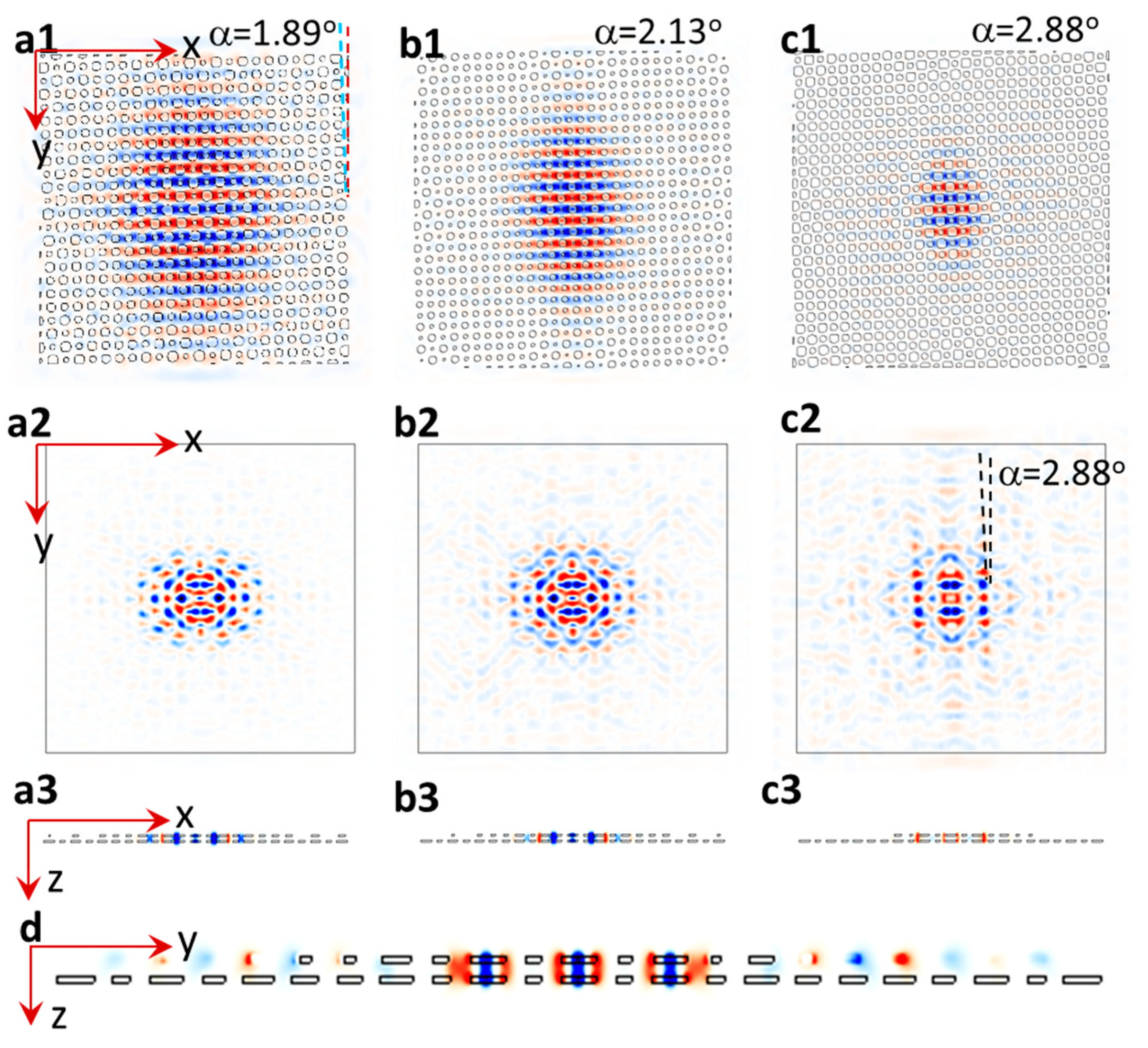
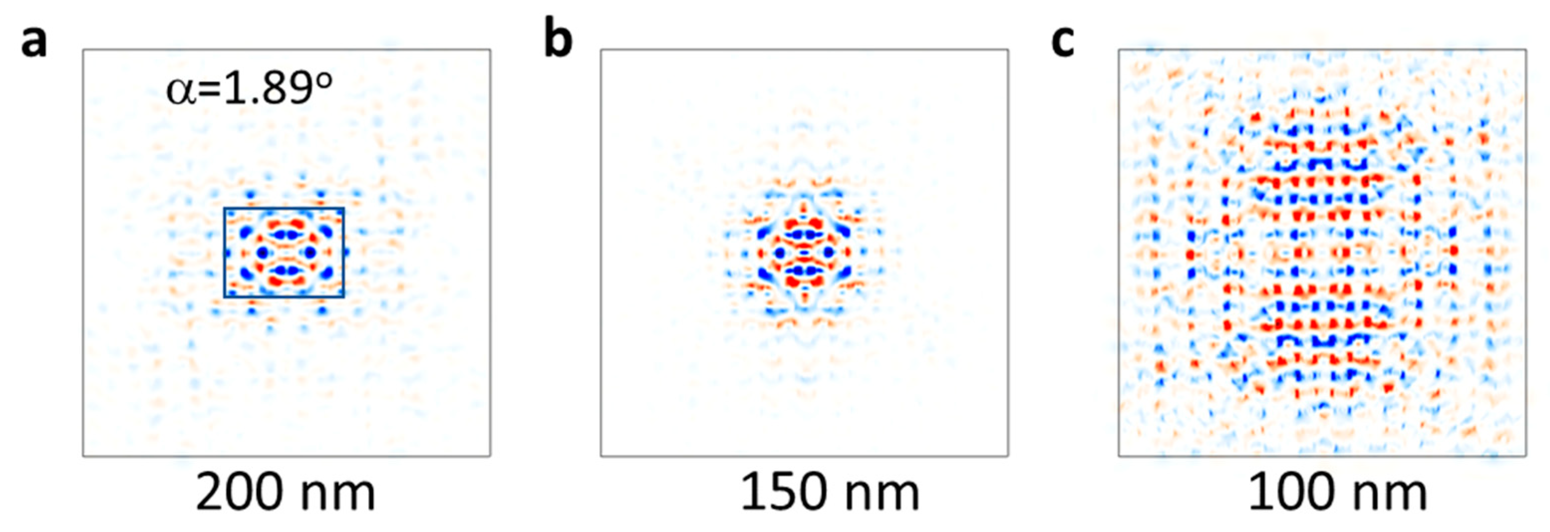
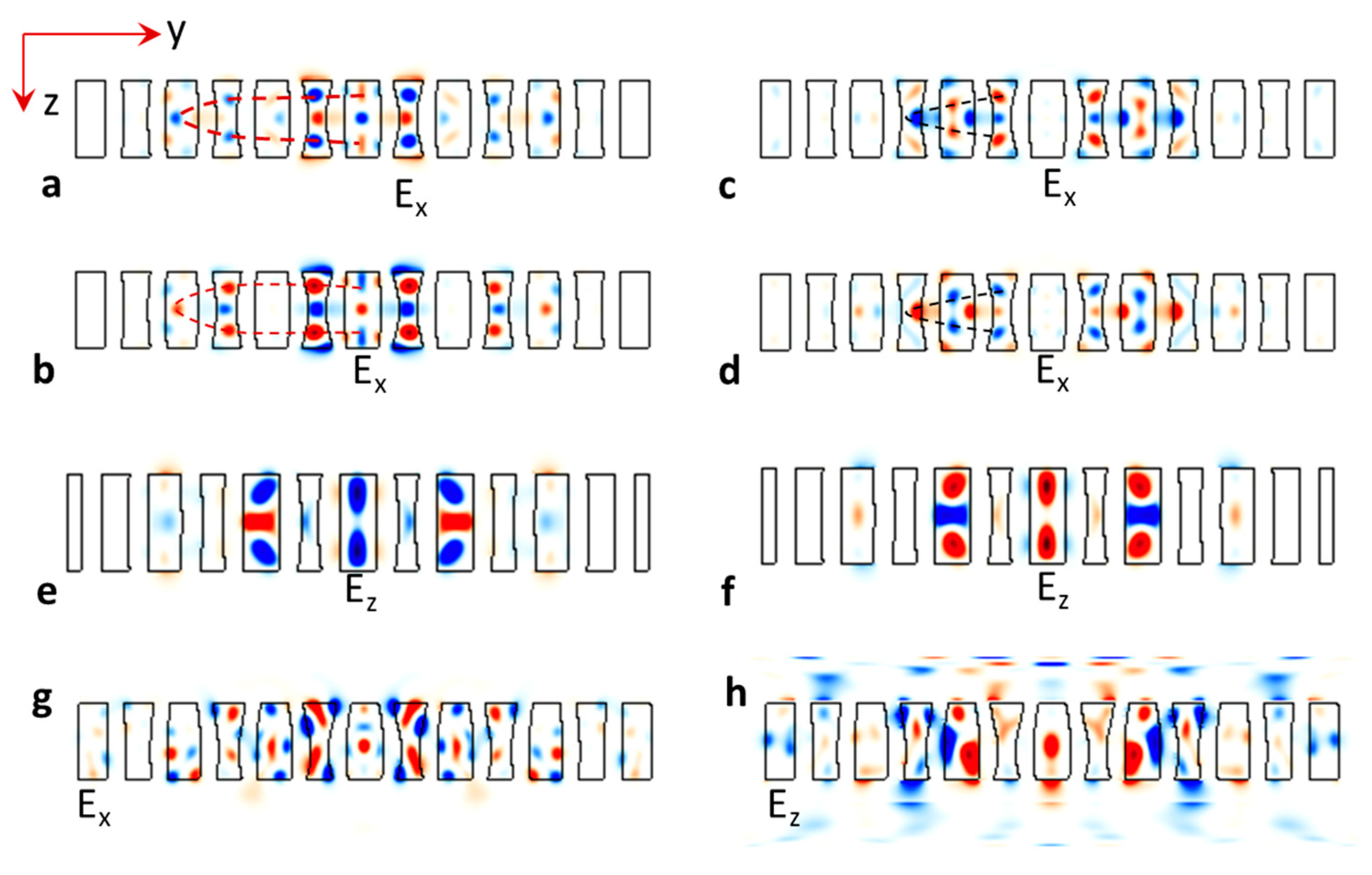
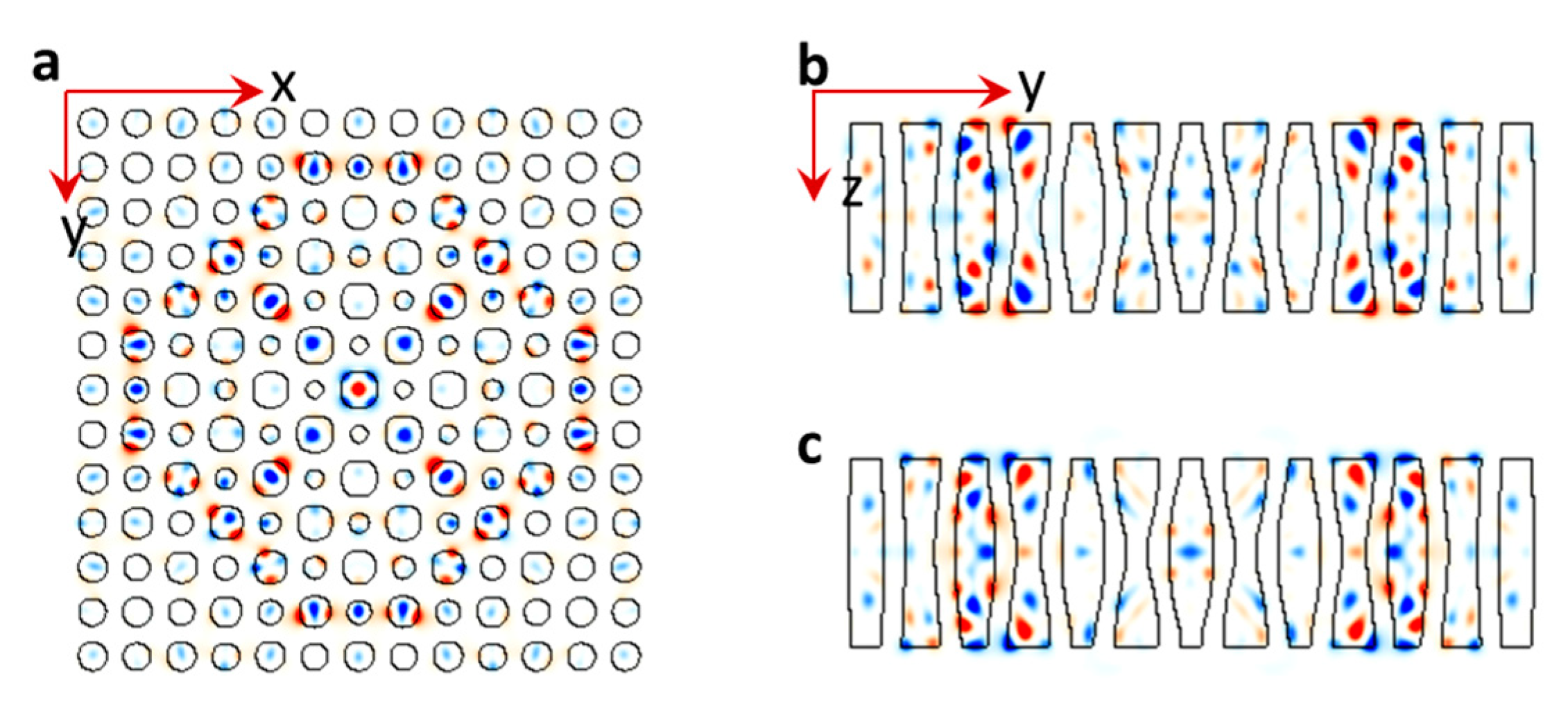
3. Results of Light Confinement in Bilayer Moiré-Over-Moiré PhCs

The bilayer moiré-over-moiré PhCs in Figure 2(a1,b1,c1) are designed following the Harvard research group design [37,38]: top moiré PhC has a thickness of 180 nm with a refractive index contrast of 3.48/1; the coupler (spacer) between two moiré PhCs has a thickness of 36 nm for a strong coupling and n = 1.48 for polymethyl methacrylate (PMMA) [38]; the bottom moiré PhC has the same structural and material parameters as the top one but is rotated by twist angles of 1.89, 2.13, and 2.88 degrees in Figure 2(a1,b1,c1), respectively. When a light source with both Ex and Ey polarization was used, there was a coupling between the top and bottom layers of PhCs. In this study, we also set a light source in an Ey polarization. The light is confined in AA-stacked region, similar to the Harvard research group results. When the twist angle increases from 1.89 to 2.13 and 2.88 degrees, the AA-stacked region becomes smaller; therefore, it is reasonable to see that the light is confined to a smaller region in Figure 2(b1) and mostly localized in Figure 2(c1).
We also calculate the E field in xy plane in twisted bilayer moiré-over-moiré PhCs for a weak-coupling case, where the top and bottom moiré layer thickness is 220 nm and the spacer thickness is 250 nm [37] for different twist angles of 1.89, 2.13, and 2.88 degrees in Figure 2(a2,b2,c2), respectively. Similar to the Harvard research group results, the light becomes less localized when the twist angle is increased from 1.89 to 2.13, and further to 2.88 degrees [37]. E-field intensity in xz-plane in Figure 2(a3,b3,c3) shows the light coupling between layers. In Figure 2(c2), the light appears outside the AA-stacked region and travels in the direction of lattice orientation of the top moiré layer, which is 2.88 degrees away from the y-axis as indicated in the figure. The cross-section view of E-field intensity in yz plane in Figure 2d shows a coupling of light in AA-stacked region and light propagation in the top moiré layer. The weak coupling of E fields between dual sublattices is also observed as the blue colors concentrated in one set of lattices in Figure 2d.
Besides the above simulations with structural parameters and twist angles from the Harvard research group [37,38], we perform more simulations on the relationship between the light confinement and spacer thickness. Starting from the structural parameters in Figure 2(a2) with (220, 250, 220) nm for the thickness of (top layer, spacer, bottom layer), we change the spacer thickness to be 200, 150, and 100 nm. The twist angle is still 1.89 degrees. Figure 3 shows the simulation results. With the thickness of 200 nm, the light is confined inside the region as indicated by a rectangle in Figure 3a, similar to the results in Figure 2(a2). There is no significant change in Figure 3b when the spacer thickness is decreased to 150 nm. However, the light confinement is very weak in Figure 3c when the spacer thickness is 100 nm. We can see that the E-field distribution looks like a dumbbell shape. With a small spacer thickness, the light confinement in the spacer is competing with those in the AA region. This can lead to an application of reconfigurable light confinement or cavity for nanophotonics by a tunable thickness or refractive index of the spacer.
Now, we keep the same layer thickness and twist angle of 1.89 degrees as those in Figure 2(a2); however, we change the material property from n = 3.48 for rod-type motif to a real p-type silicon for top and bottom layers. Figure 4a shows the E-field intensity in xy plane in twisted bilayer moiré-over-moiré PhC with layer thicknesses of (220, 250, 220 nm) at times of 8/24 (Figure 4a1) and 16/24 (Figure 4(a2)) of one time period when the E-field intensity switches color from red-blue (Figure 4(a1)) to blue-red (Figure 4(a2)). There are more modes confined inside or outside the rectangle in Figure 4(a1) than those in Figure 2(a2) and Figure 3a (the rectangle is not drawn and mode numbers are compared). It seems that the real silicon has a dispersion that can meet the requirement of resonance condition for more modes.
We assume that a small thickness of the spacer relative to that in the top or bottom layer in Figure 2(a1) and Figure 3c leads to a weak light confinement. We increase the thickness to 455 nm for the top and bottom layers, keep the same thickness of 36 nm for the spacer, and change the material property from n = 3.48 for the rod-type motif to a real p-type silicon for the top and bottom layers. Figure 4(b1,b2) shows the E-field intensity in xz plane in the twisted bilayer moiré-over-moiré PhC at times of 1/24 (Figure 4(b1)) and 9/24 (Figure 4(b2)) of one time period, respectively. Figure 4c shows the E-field intensity in yz plane in the same structure as (Figure 4b). With a large thickness in the top and bottom layers, the light is confined in the middle of the structure. The total thickness of 455 nm for the top layer and 455 nm for the bottom layer is close to half of the z-modulation period in Figure 1c. The fabrication of twisted PhCs has used a complex process of E-beam lithography patterning, SU-8 based suspending, spacing, and bonding [26]. Instead of further studying the multi-layer moiré-over-moiré PhCs, we turn to a single-layer 2D+ moiré silicon PhC in the next section. Furthermore, it may not be easy to directly integrate the bilayer moiré PhCs in a nanophotonic device; however, a single-layer 2D+ moiré silicon PhC is as easy as a conventional PhC for nanophotonics integration. A very recent publication [56] in reconfigurable moiré laser further stimulates this research.

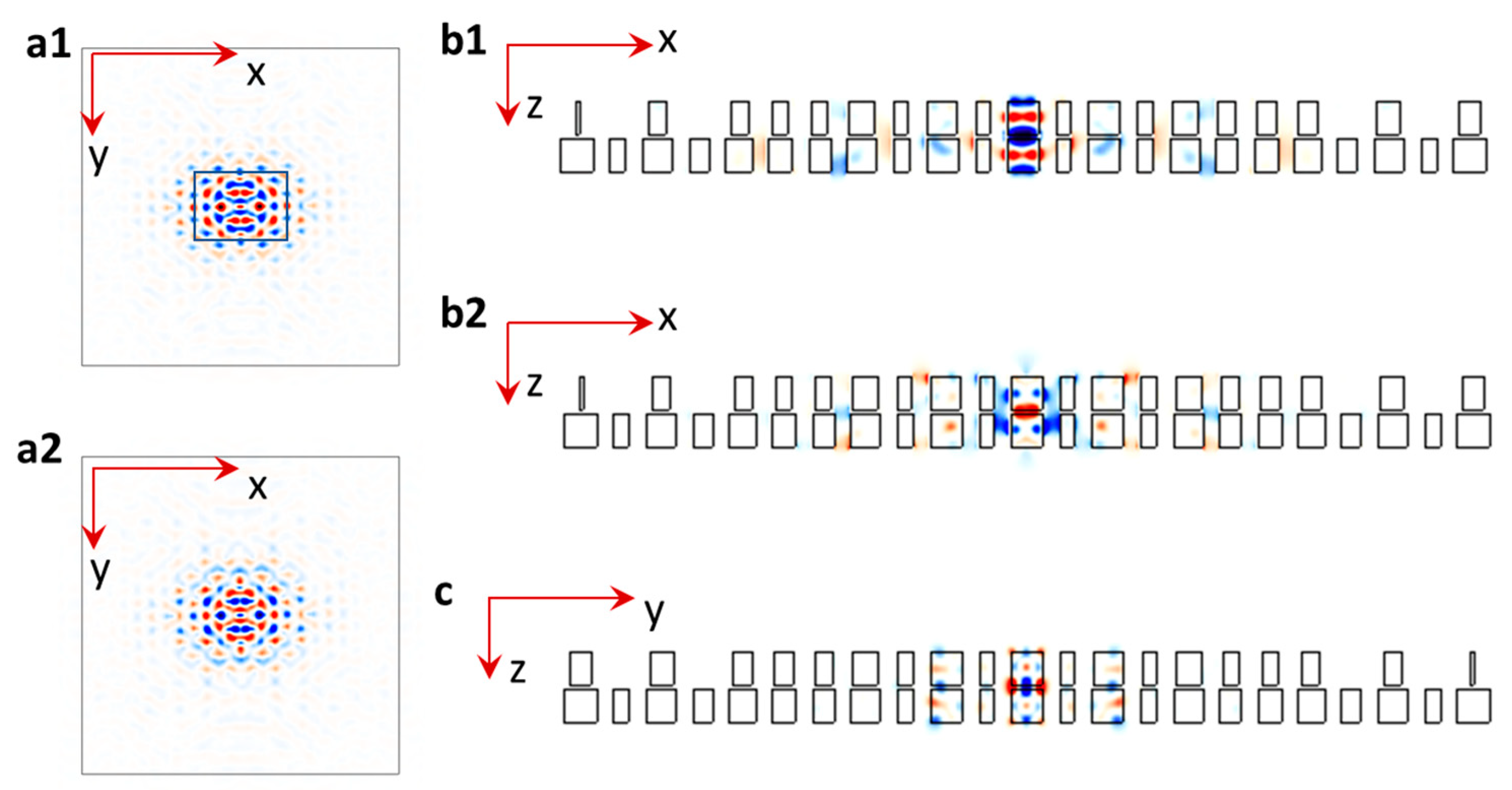
4. Results of Light Confinement in 2D+ Moiré Silicon PhCs

The fabrication of a single-layer 2D+ moiré silicon can start from a thick photoresist of SU-8 instead of dipentaerythritol penta-/hexa-acrylate (DPHPA), which is recently used for 3D moiré PhCs [52,53]. The eight-beam interference pattern can be recorded in SU-8, which can be post exposure baked and developed. The developed PhCs in SU-8 can be filled with SiO2, and then burn away SU-8. Thereafter, PhCs in SiO2 can be filled with silicon and SiO2 is etched away (a double-conversion process) [57]. We set the thickness of 2D+ moiré silicon PhCs to be half of the z-modulation period. The simulated E-field intensity has been outputted into 20 images at the (1/20), (2/20), (3/20) … (20/20) step of one time period. Figure 5a,b shows the E-field intensity in 2D+ moiré silicon PhCs in two of the above moments when their intensities are switched, i.e., the blue color becomes red while the red color becomes blue. In the central regions, the motif in single-layer moiré PhC looks like an alternative concave and convex lens. As indicated by the red dashed line, the light in Ex polarization is converged into a point as it travels from the central region to the left in Figure 5a,b. In Figure 5c,d, the red color switches to a blue color and the light source in Ex polarization is converged as indicated by the red dashed line. Figure 5e,f shows the E-field intensity in zy plane in twisted single-layer moiré PhC with a thickness equal to half of the z-modulation period in pairs that switch the E-field strength in Ez polarization during oscillations. They look like a standing wave with top and bottom edges as boundaries. If the single-layer moiré PhCs are fabricated on a substrate, these modes will radiate into the substrate and air as shown below.
Figure 5g,h shows the E-field intensity in zy plane for polarization Ex and Ez, respectively, in a twisted single-layer moiré PhC with a thickness equal to half of the z-modulation period on a 500 nm glass substrate. The oscillation modes in both figures maintain a mirror symmetry along y = 0; however, they do not have a mirror symmetry along z = 0 as expected. It is clearly observed that the light source in Ex polarization is localized in the single-layer moiré PhC; however, the localization cannot sustain the Ez polarization in Figure 5h.

5. Discussion

In the simulation, we have used a resolution of 24 (relatively low) due to the large 3D unit super-cell size. In both fabrications and simulations, a thin single-layer moiré PhC is favored. Although the simulation of resonance modes and calculation of their Q-factors were not in high resolutions, we observed a trend of increasing Q-factors with an increasing thickness of single-layer moiré PhCs. The maximum Q-factor for resonance modes with Ex polarization is in the magnitude order of 103 for single-layer moiré PhCs with a thickness of 0.5 z-modulation period, while it is in the order of 104 when the thickness is one z-modulation period. Figure 6a–c show the E-field intensity in xy plane and zy planefor polarization Ex in twisted single-layer 2D+ moiré PhC with a thickness of one z-modulation period. Although it is a relatively low-resolution simulation, resonance modes are clearly visible and symmetric. As expected, the E field is propagating along the same set of sublattices. In the zy plane in Figure 6b,c, the resonance mode is not a standing wave in z direction and can survive when the single-layer 2D+ moiré PhCs are fabricated on a glass substrate.
The validation of simulation results is necessary as in recent applications [56]. The simulated E-field propagation along the same set of sublattices in Figure 5a,b,e corresponds to the disappearance of first-order diffraction spots that have recently been observed in experiments [48]. Next, we should work on the fabrication of single-layer 2D+ moiré PhCs in silicon through the double-conversion process described above [57]. For a lasing application of single-layer moiré PhCs in an active medium, the integration of 2D layered materials on moiré PhCs can be studied.

6. Conclusions

We have studied light confinement in bilayer twisted moiré-overlapping-moiré PhCs and single-layer 2D+ moiré PhCs. In weak-coupling moiré-overlapping-moiré PhCs, the light source is less localized with an increasing twist angle, while the light source is tightly localized with an increasing twist angle in the strong-coupling case. For the single-layer 2D+ moiré PhCs, the light source with Ez polarization cannot survive when the PhCs are integrated on a glass substrate. Lens effects and resonance modes are observed for the light source with Ex polarization in single-layer 2D+ moiré PhCs. Most importantly, we conclude that single-layer 2D+ moiré PhCs are very promising and ready for integration in nanophotonic devices.

Author Contributions

Conceptualization, Y.L., J.C. and A.B.K.; methodology, S.K., N.H.,Y.L. and J.C.; software, S.K., N.H. and Y.L.; investigation, S.K., N.H. and Y.L.; formal analysis, Y.L. and S.K.; writing—original draft preparation, S.K. and Y.L.; writing—review and editing, all authors; funding acquisition, A.B.K., J.C. and Y.L. All authors have read and agreed to the published version of the manuscript.

Funding

This research was partially supported by the US National Science Foundation, grant number 2128367 and by the Department of Energy/National Nuclear Security Administration under Award Number DE-NA0004114. This report was prepared as an account of work sponsored by an agency of the United States Government. Neither the United States Government nor any agency thereof, nor any of their employees, makes any warranty, express or implied, or assumes any legal liability or responsibility for the accuracy, completeness, or usefulness of any information, apparatus, product, or process disclosed, or represents that its use would not infringe privately owned rights. Reference herein to any specific commercial product, process, or service by trade name, trademark, manufacturer, or otherwise does not necessarily constitute or imply its endorsement, recommendation, or favoring by the United States Government or any agency thereof. The views and opinions of authors expressed herein do not necessarily state or reflect those of the United States Government or any agency thereof.

Informed Consent Statement

Not applicable.

Data Availability Statement

The data presented in this study are available on request from the corresponding author. The data are not publicly available due to limited access to Amazon Web Service.

Conflicts of Interest

The authors declare no conflict of interest.

References

  1. Cao, Y.; Fatemi, V.; Fang, S.; Watanabe, K.; Taniguchi, T.; Kaxiras, E.; Jarillo-Herrero, P. Unconventional Superconductivity in Magic-Angle Graphene Superlattices. Nature 2018, 556, 43–50. [Google Scholar] [CrossRef]
  2. Yankowitz, M.; Chen, S.; Polshyn, H.; Zhang, Y.; Watanabe, K.; Taniguchi, T.; Graf, D.; Young, A.F.; Dean, C.R. Tuning Superconductivity in Twisted Bilayer Graphene. Science 2019, 363, 1059–1064. [Google Scholar] [CrossRef] [PubMed]
  3. Balents, L.; Dean, C.R.; Efetov, D.K.; Young, A.F. Superconductivity and Strong Correlations in Moiré Flat Bands. Nat. Phys. 2020, 16, 725–733. [Google Scholar] [CrossRef]
  4. Arora, H.S.; Polski, R.; Zhang, Y.; Thomson, A.; Choi, Y.; Kim, H.; Lin, Z.; Wilson, I.Z.; Xu, X.; Chu, J.-H.; et al. Superconductivity in Metallic Twisted Bilayer Graphene Stabilized by WSe2. Nature 2020, 583, 379–384. [Google Scholar] [CrossRef] [PubMed]
  5. González, J.; Stauber, T. Kohn-Luttinger Superconductivity in Twisted Bilayer Graphene. Phys. Rev. Lett. 2019, 122, 026801. [Google Scholar] [CrossRef] [PubMed]
  6. Uri, A.; de la Barrera, S.C.; Randeria, M.T.; Rodan-Legrain, D.; Devakul, T.; Crowley, P.J.D.; Paul, N.; Watanabe, K.; Taniguchi, T.; Lifshitz, R.; et al. Superconductivity and Strong Interactions in a Tunable Moiré Quasicrystal. Nature 2023, 620, 762–767. [Google Scholar] [CrossRef]
  7. Uchida, K.; Furuya, S.; Iwata, J.-I.; Oshiyama, A. Atomic Corrugation and Electron Localization Due to Moiré Patterns in Twisted Bilayer Graphenes. Phys. Rev. B 2014, 90, 155451. [Google Scholar] [CrossRef]
  8. Sunku, S.S.; Ni, G.X.; Jiang, B.Y.; Yoo, H.; Sternbach, A.; McLeod, A.S.; Stauber, T.; Xiong, L.; Taniguchi, T.; Watanabe, K.; et al. Photonic Crystals for Nano-Light in Moiré Graphene Superlattices. Science 2018, 362, 1153–1156. [Google Scholar] [CrossRef]
  9. Wu, F.; Lovorn, T.; Tutuc, E.; Martin, I.; MacDonald, A.H. Topological Insulators in Twisted Transition Metal Dichalcogenide Homobilayers. Phys. Rev. Lett. 2019, 122, 086402. [Google Scholar] [CrossRef]
  10. Bai, Y.; Zhou, L.; Wang, J.; Wu, W.; McGilly, L.J.; Halbertal, D.; Lo, C.F.B.; Liu, F.; Ardelean, J.; Rivera, P.; et al. Excitons in Strain-Induced One-Dimensional Moiré Potentials at Transition Metal Dichalcogenide Heterojunctions. Nat. Mater. 2020, 19, 1068–1073. [Google Scholar] [CrossRef]
  11. Zhang, Z.; Wang, Y.; Watanabe, K.; Taniguchi, T.; Ueno, K.; Tutuc, E.; LeRoy, B.J. Flat Bands in Twisted Bilayer Transition Metal Dichalcogenides. Nat. Phys. 2020, 16, 1093–1096. [Google Scholar] [CrossRef]
  12. Naik, M.H.; Jain, M. Ultraflatbands and Shear Solitons in Moiré Patterns of Twisted Bilayer Transition Metal Dichalcogenides. Phys. Rev. Lett. 2018, 121, 266401. [Google Scholar] [CrossRef] [PubMed]
  13. Mullan, C.; Slizovskiy, S.; Yin, J.; Wang, Z.; Yang, Q.; Xu, S.; Yang, Y.; Piot, B.A.; Hu, S.; Taniguchi, T.; et al. Mixing of Moiré-Surface and Bulk States in Graphite. Nature 2023, 620, 756–761. [Google Scholar] [CrossRef] [PubMed]
  14. Liu, S.; Ma, S.; Shao, R.; Zhang, L.; Yan, T.; Ma, Q.; Zhang, S.; Cui, T.J. Moiré Metasurfaces for Dynamic Beamforming. Sci. Adv. 2022, 8, eabo1511. [Google Scholar] [CrossRef] [PubMed]
  15. Hu, G.; Wang, M.; Mazor, Y.; Qiu, C.-W.; Alù, A. Tailoring Light with Layered and Moiré Metasurfaces. Trends Chem. 2021, 3, 342–358. [Google Scholar] [CrossRef]
  16. Hu, G.; Krasnok, A.; Mazor, Y.; Qiu, C.-W.; Alù, A. Moiré Hyperbolic Metasurfaces. Nano Lett. 2020, 20, 3217–3224. [Google Scholar] [CrossRef] [PubMed]
  17. Alnasser, K.; Kamau, S.; Hurley, N.; Cui, J.; Lin, Y. Resonance Modes in Moiré Photonic Patterns for Twistoptics. OSA Contin. 2021, 4, 1339. [Google Scholar] [CrossRef]
  18. Duan, J.; Capote-Robayna, N.; Taboada-Gutiérrez, J.; Álvarez-Pérez, G.; Prieto, I.; Martín-Sánchez, J.; Nikitin, A.Y.; Alonso-González, P. Twisted Nano-Optics: Manipulating Light at the Nanoscale with Twisted Phonon Polaritonic Slabs. Nano Lett. 2020, 20, 5323–5329. [Google Scholar] [CrossRef]
  19. Lin, H.-M.; Lu, Y.-H.; Chang, Y.-J.; Yang, Y.-Y.; Jin, X.-M. Direct Observation of a Localized Flat-Band State in a Mapped Moiré Hubbard Photonic Lattice. Phys. Rev. Appl. 2022, 18, 054012. [Google Scholar] [CrossRef]
  20. Dong, K.; Zhang, T.; Li, J.; Wang, Q.; Yang, F.; Rho, Y.; Wang, D.; Grigoropoulos, C.P.; Wu, J.; Yao, J. Flat Bands in Magic-Angle Bilayer Photonic Crystals at Small Twists. Phys. Rev. Lett. 2021, 126, 223601. [Google Scholar] [CrossRef]
  21. Yi, C.-H.; Park, H.C.; Park, M.J. Strong Interlayer Coupling and Stable Topological Flat Bands in Twisted Bilayer Photonic Moiré Superlattices. Light Sci. Appl. 2022, 11, 289. [Google Scholar] [CrossRef] [PubMed]
  22. Mao, X.-R.; Shao, Z.-K.; Luan, H.-Y.; Wang, S.-L.; Ma, R.-M. Magic-Angle Lasers in Nanostructured Moiré Superlattice. Nat. Nanotechnol. 2021, 16, 1099–1105. [Google Scholar] [CrossRef] [PubMed]
  23. Nguyen, D.X.; Letartre, X.; Drouard, E.; Viktorovitch, P.; Nguyen, H.C.; Nguyen, H.S. Magic Configurations in Moiré Superlattice of Bilayer Photonic Crystals: Almost-Perfect Flatbands and Unconventional Localization. Phys. Rev. Res. 2022, 4, L032031. [Google Scholar] [CrossRef]
  24. Wang, H.; Ma, S.; Zhang, S.; Lei, D. Intrinsic Superflat Bands in General Twisted Bilayer Systems. Light Sci. Appl. 2022, 11, 159. [Google Scholar] [CrossRef] [PubMed]
  25. Zhou, J.; Xie, S.; Nie, C.; Xu, P.; Yi, J.; Liu, E. Optical Properties of a Moiré-Lattice Photonic Crystal Fiber with Controllable Magic Angle. Results Phys. 2023, 51, 106659. [Google Scholar] [CrossRef]
  26. Tang, H.; Lou, B.; Du, F.; Zhang, M.; Ni, X.; Xu, W.; Jin, R.; Fan, S.; Mazur, E. Experimental Probe of Twist Angle–Dependent Band Structure of on-Chip Optical Bilayer Photonic Crystal. Sci. Adv. 2023, 9, eadh8498. [Google Scholar] [CrossRef] [PubMed]
  27. Lou, B.; Wang, B.; Rodríguez, J.A.; Cappelli, M.; Fan, S. Tunable Guided Resonance in Twisted Bilayer Photonic Crystal. Sci. Adv. 2022, 8, eadd4339. [Google Scholar] [CrossRef]
  28. Lou, B.; Zhao, N.; Minkov, M.; Guo, C.; Orenstein, M.; Fan, S. Theory for Twisted Bilayer Photonic Crystal Slabs. Phys. Rev. Lett. 2021, 126, 136101. [Google Scholar] [CrossRef]
  29. Huang, L.; Zhang, W.; Zhang, X. Moiré Quasibound States in the Continuum. Phys. Rev. Lett. 2022, 128, 253901. [Google Scholar] [CrossRef]
  30. Hu, G.; Zheng, C.; Ni, J.; Qiu, C.-W.; Alù, A. Enhanced Light-Matter Interactions at Photonic Magic-Angle Topological Transitions. Appl. Phys. Lett. 2021, 118, 211101. [Google Scholar] [CrossRef]
  31. Krasnok, A.; Alù, A. Low-Symmetry Nanophotonics. ACS Photonics 2022, 9, 2–24. [Google Scholar] [CrossRef]
  32. Chen, J.; Lin, X.; Chen, M.; Low, T.; Chen, H.; Dai, S. A Perspective of Twisted Photonic Structures. Appl. Phys. Lett. 2021, 119, 240501. [Google Scholar] [CrossRef]
  33. Wu, Z.; Zheng, Y. Moiré Chiral Metamaterials. Adv. Opt. Mater. 2017, 5, 1700034. [Google Scholar] [CrossRef]
  34. Lou, B.; Fan, S. Tunable frequency filter based on twisted bilayer photonic crystal slabs. ACS Photonics 2022, 9, 800–805. [Google Scholar] [CrossRef]
  35. Zhang, T.; Dong, K.; Li, J.; Meng, F.; Li, J.; Munagavalasa, S.; Grigoropoulos, C.P.; Wu, J.; Yao, J. Twisted Moiré Photonic Crystal Enabled Optical Vortex Generation through Bound States in the Continuum. Nat. Commun. 2023, 14, 6014. [Google Scholar] [CrossRef] [PubMed]
  36. Meng, Z.; Wang, L.; Han, W.; Liu, F.; Wen, K.; Gao, C.; Wang, P.; Chin, C.; Zhang, J. Atomic Bose–Einstein condensate in twisted-bilayer optical lattices. Nature 2023, 615, 231–236. [Google Scholar] [CrossRef] [PubMed]
  37. Tang, H.; Du, F.; Carr, S.; DeVault, C.; Mello, O.; Mazur, E. Modeling the Optical Properties of Twisted Bilayer Photonic Crystals. Light Sci. Appl. 2021, 10, 157. [Google Scholar] [CrossRef] [PubMed]
  38. Tang, H.; Ni, X.; Du, F.; Srikrishna, V.; Mazur, E. On-Chip Light Trapping in Bilayer Moiré Photonic Crystal Slabs. Appl. Phys. Lett. 2022, 121, 231702. [Google Scholar] [CrossRef]
  39. Zeng, J.; Hu, Y.; Zhang, X.; Fu, S.; Yin, H.; Li, Z.; Chen, Z. Localization-to-Delocalization Transition of Light in Frequency-Tuned Photonic Moiré Lattices. Opt. Express 2021, 29, 25388. [Google Scholar] [CrossRef]
  40. Fu, Q.; Wang, P.; Huang, C.; Kartashov, Y.V.; Torner, L.; Konotop, V.V.; Ye, F. Optical Soliton Formation Controlled by Angle Twisting in Photonic Moiré Lattices. Nat. Photonics 2020, 14, 663–668. [Google Scholar] [CrossRef]
  41. Talukdar, T.H.; Hardison, A.L.; Ryckman, J.D. Moiré Effects in Silicon Photonic Nanowires. ACS Photonics 2022, 9, 1286–1294. [Google Scholar] [CrossRef]
  42. Zhou, X.; Lin, Z.; Lu, W.; Lai, Y.; Hou, B.; Jiang, J. Twisted Quadrupole Topological Photonic Crystals. Laser Photon Rev. 2020, 14, 2000010. [Google Scholar] [CrossRef]
  43. Shang, C.; Lu, C.; Tang, S.; Gao, Y.; Wen, Z. Generation of Gradient Photonic Moiré Lattice Fields. Opt. Express 2021, 29, 29116. [Google Scholar] [CrossRef] [PubMed]
  44. Han, J.-H.; Kim, I.; Ryu, J.-W.; Kim, J.; Cho, J.-H.; Yim, G.-S.; Park, H.-S.; Min, B.; Choi, M. Rotationally Reconfigurable Metamaterials Based on Moiré Phenomenon. Opt. Express 2015, 23, 17443. [Google Scholar] [CrossRef] [PubMed]
  45. Wang, P.; Zheng, Y.; Chen, X.; Huang, C.; Kartashov, Y.V.; Torner, L.; Konotop, V.V.; Ye, F. Localization and Delocalization of Light in Photonic Moiré Lattices. Nature 2020, 577, 42–46. [Google Scholar] [CrossRef] [PubMed]
  46. Kartashov, Y.V.; Ye, F.; Konotop, V.V.; Torner, L. Multifrequency Solitons in Commensurate-Incommensurate Photonic Moiré Lattices. Phys. Rev. Lett. 2021, 127, 163902. [Google Scholar] [CrossRef] [PubMed]
  47. Khurgin, J.B. Light Slowing down in Moiré Fiber Gratings and Its Implications for Nonlinear Optics. Phys. Rev. A 2000, 62, 013821. [Google Scholar] [CrossRef]
  48. Alnasser, K.; Li, S.; Sidhik, S.; Kamau, S.; Hou, J.; Hurley, N.; Alzaid, A.; Wang, S.; Yan, H.; Deng, J.; et al. Fabrication of Twisted Moire Photonic Crystal and Random Moire Photonic Crystal and Their Potential Applications in Light Extraction. Nanotechnology 2024, 35, 025203. [Google Scholar] [CrossRef]
  49. Lowell, D.; Lutkenhaus, J.; George, D.; Philipose, U.; Chen, B.; Lin, Y. Simultaneous Direct Holographic Fabrication of Photonic Cavity and Graded Photonic Lattice with Dual Periodicity, Dual Basis, and Dual Symmetry. Opt. Express 2017, 25, 14444. [Google Scholar] [CrossRef]
  50. Lowell, D.; Hassan, S.; Adewole, M.; Philipose, U.; Chen, B.; Lin, Y. Holographic Fabrication of Graded Photonic Super-Crystals Using an Integrated Spatial Light Modulator and Reflective Optical Element Laser Projection System. Appl. Opt. 2017, 56, 9888. [Google Scholar] [CrossRef]
  51. Ohlinger, K.; Lutkenhaus, J.; Arigong, B.; Zhang, H.; Lin, Y. Spatially Addressable Design of Gradient Index Structures through Spatial Light Modulator Based Holographic Lithography. J. Appl. Phys. 2013, 114, 213102. [Google Scholar] [CrossRef]
  52. Hurley, N.; Kamau, S.; Alnasser, K.; Philipose, U.; Cui, J.; Lin, Y. Laser Diffraction Zones and Spots from Three-Dimensional Graded Photonic Super-Crystals and Moiré Photonic Crystals. Photonics 2022, 9, 395. [Google Scholar] [CrossRef]
  53. Hurley, N.; Kamau, S.; Cui, J.; Lin, Y. Holographic Fabrication of 3D Moiré Photonic Crystals Using Circularly Polarized Laser Beams and a Spatial Light Modulator. Micromachines 2023, 14, 1217. [Google Scholar] [CrossRef] [PubMed]
  54. Gorgulu, K.; Gok, A.; Yilmaz, M.; Topalli, K.; Bıyıklı, N.; Okyay, A.K. All-Silicon Ultra-Broadband Infrared Light Absorbers. Sci. Rep. 2016, 6, 38589. [Google Scholar] [CrossRef]
  55. Oskooi, A.F.; Roundy, D.; Ibanescu, M.; Bermel, P.; Joannopoulos, J.D.; Johnson, S.G. MEEP: A Flexible Free-Software Package for Electromagnetic Simulations by the FDTD Method. Comput. Phys. Commun. 2010, 181, 687–702. [Google Scholar] [CrossRef]
  56. Luan, H.Y.; Ouyang, Y.H.; Zhao, Z.W.; Mao, W.Z.; Ma, R.M. Reconfigurable moiré nanolaser arrays with phase synchronization. Nature 2023, 624, 282–288. [Google Scholar] [CrossRef]
  57. Tétreault, N.; Freymann, G.V.; Deubel, M.; Hermatschweiler, M.; Willard, F.P.; John, S.; Wegener, M.; Ozin, G.A. New route to three-dimensional photonic bandgap materials: Silicon double inversion of polymer templates. Adv. Mater. 2006, 18, 457. [Google Scholar] [CrossRef]
Figure 1. (a) Photo of eight green laser spots at the Fourier filter plane and schematic of their wavevectors, wavevector differences, and rotation by an angle of α. (b) Twisted moiré pattern from eight beam laser interferences in xy plane with a super-cell size of 12Plattice × 12Plattice. (c) Eight beam laser interference patterns in the xz plane with one period thickness in z direction. (d) Permittivity structure generated from MEEP simulation for 2D moiré pattern with a certain thickness. (e) The 2D moiré pattern overlapping and rotating by an angle of 5 degrees on another 2D moiré pattern.
Photonics 11 00013 g001
Figure 2. The twist angles for bilayer moiré PhCs are 1.89, 2.13, and 2.88 degrees for figures in column I, II, and III, respectively. (0,0,z), (x,0,0) or (0,y,0) is at the center of each figure. (a1,b1,c1) E-field intensity in xy plane in twisted bilayer moiré-over-moiré PhC where the thicknesses of the top moiré layer, spacer, and bottom moiré layer are 180, 36, and 180 nm, respectively. (a2,b2,c2) E-field intensity in xy plane in twisted bilayer moiré-over-moiré PhC with layer thicknesses of 220, 250, and 220 nm, respectively. (a3,b3,c3) E-field intensity in xz plane as viewed along y = 0 in twisted bilayer moiré-over-moiré PhC in (a2,b2,c2), respectively. (d) E-field intensity in yz plane as viewed along x = 0 in (c2).
Photonics 11 00013 g002
Figure 3. (ac) E-field intensity in xy plane in twisted bilayer moiré-over-moiré PhC with layer thicknesses of (220, spacer, 220 nm) where spacer = 200 nm (a), 150 nm (b) and 100 nm (c), respectively. The twist angle for bilayer moiré PhCs is 1.89 degrees for all figures. (0,0,z) is at the center of each figure.
Photonics 11 00013 g003
Figure 4. (a1,a2) E-field intensity in xy plane in twisted bilayer moiré-over-moiré PhC with layer thicknesses of (220, 250, 220 nm) for top layer, spacer, and bottom layer at times of 8/24 (a1) and 16/24 (a2) of one time period. The twist angle for bilayer moiré PhCs is 1.89 degrees. (0,0,z) is at the center of each figure. (b1,b2) E-field intensity in xz plane in twisted bilayer moiré-over-moiré PhC with layer thicknesses of (455, 36, 455 nm) for top layer, spacer, and bottom layer at times of 1/24 (b1) and 9/24 (b2) of one time period. (c) E-field intensity in yz plane in the same structure as (b1,b2). The twist angle for bilayer moiré PhCs is 1.89 degrees. (0,0,z) (a1,a2), (0,y,0) (b1,b2) or (x,0,0) (c) is at the center of each figure.
Photonics 11 00013 g004
Figure 5. E-field intensity in zy plane in twisted single-layer 2D+ moiré PhC with a thickness of 0.5 z-modulation period in pairs that switch the E-field strength in Ex polarization during oscillations in (a,b) and (c,d) and pairs that switch the E-field strength in Ez polarization during oscillations in (e,f). (g,h) E-field intensity in zy plane for polarization Ex (g) and Ez (h) in twisted single-layer 2D+ moiré PhC with a thickness of 0.5 z-modulation period on 500 nm glass substrate.
Photonics 11 00013 g005
Figure 6. (a) E-field intensity with Ex polarization in xy plane in twisted single-layer 2D+ moiré PhC with a thickness of one z-modulation period. (b,c) E-field intensity with Ex polarization in zy plane in twisted single-layer 2D+ moiré PhC with a thickness of one z-modulation period in pairs that switch the E-field strength.
Photonics 11 00013 g006
Disclaimer/Publisher’s Note: The statements, opinions and data contained in all publications are solely those of the individual author(s) and contributor(s) and not of MDPI and/or the editor(s). MDPI and/or the editor(s) disclaim responsibility for any injury to people or property resulting from any ideas, methods, instructions or products referred to in the content.

