Article

Numerical Optimization Technique of Multilayer SERS Substrates

1
Scientific-Manufacturing Complex “Technological Centre”, 124498 Moscow, Russia
2
Technological Research Institute, Ulyanovsk State University, 432017 Ulyanovsk, Russia
*
Author to whom correspondence should be addressed.
Photonics 2024, 11(1), 12; https://doi.org/10.3390/photonics11010012
Submission received: 17 November 2023 / Revised: 21 December 2023 / Accepted: 23 December 2023 / Published: 25 December 2023
(This article belongs to the Section Optoelectronics and Optical Materials)

Abstract

:
A numerical optimization technique of a three-dimensional (3D) SERS substrate with finite element analysis is proposed. Using the optical reciprocity theorem, we have shown that instead of the well-known local field enhancement criterion, it is more correct to use the Purcell factor as an objective function that determines the quality of the SERS substrate. This allows us to take into account the detail inhomogeneity of local fields in an arbitrary three-dimensional structure containing multiple emitters. We have theoretically shown that employment of a 3D CNT structure as a nanoparticle substrate instead of a nanoparticle monolayer allows one to achieve the enhancement of the SERS signal.

1. Introduction

Today, many approaches to the formation of SERS-active layers are known. The most commonly used are: chemical methods for the formation of metal (plasmonic) nanoparticles in colloidal solutions with the subsequent deposition of nanoparticles onto a solid substrate; physical methods of deposition of thin films transforming by heating into an ensemble of self-organized nanoparticles; as well as the use of lithographic methods for the formation of nanoobjects of various shapes. Complex nanostructured surfaces, various arrays of micro- or nanopillars, nanorods, and nanotubes have already been used as substrates for SERS-active layers [1,2,3]. The main goal is the formation of so-called “hot spots”—regions with a high local density of states [4,5,6,7,8,9,10,11,12,13,14], leading to the magnification of Raman scattering [15].
To optimize the production of the SERS substrates, the geometric parameters can be improved by using numerical methods [16]. The SERS occurs only when the scattering molecule is located closer than ten nanometers to the nanoantenna, which complicates theoretical description. At such distances, the interaction can be originated by several mechanisms: electromagnetic enhancement [17] as well as changes in the electronic shells of the SERS molecule and the underlying medium [18]. Strictly speaking, a rigorous theoretical description of the SERS effect must be a quantum one. This research direction is observed in refs. [18,19,20].
Due to the extremely high practical significance of the effect, the efforts of experimental groups [21,22,23] are more often aimed at applied aspects [24], but not at studying the fundamental features of the effect. These works seldom differentiate various mechanisms of the analyzed molecule emission rate increase, located in an inhomogeneous environment.
The vast majority of papers aimed at numerical optimization of SERS substrates focus on maximizing the local field [16,25,26,27,28,29]. Such an approach considers the field at the location of the detected molecule and only indirectly reveals the SERS enhancement of complex structures. It takes into account only the local field acting on the molecule, which provides information about the radiation scattered in the close vicinity of the analyzed molecule but says nothing about the actually detected radiation in the far zone. Searching for the “hot spots” and assessing the local fields at these points can only provide relevant information about the SERS signal in simple cases when all emitters are to some extent under similar conditions and the field intensity at the different “hot spots” is therefore the same or can be averaged [16,24]. This is the case only for two-dimensional SERS substrates [16].
Attempts to create multilayer three-dimensional SERS substrates [1,26], proposed to improve the integral signal by increasing the number of “hot spots”, are generating considerable interest. One of the methods for producing the 3D SERS structures is to coat the available 3D matrices (semiconductor nanowires, porous structures of Si, TiO2, Al2O3) with plasmonic metal nanoparticles, where the matrix defines the disposition of nanoparticles in such a way that the number of “hot spots” is enlarged [15,30,31,32]. The result [30,33] shows, however, that the increase in the SERS layers’ number leads to saturation of the signal due to absorption of the electromagnetic wave by plasmonic structures. The last point shows that the numerical optimization of the SERS substrates, which are more complex than 2D ones [1,33], requires rather sophisticated methods.
The aim of this work is to propose a method for calculating the optical signal for three-dimensional SERS substrates and to study the possibility of scaling the SERS signal using three-dimensional substrates. The paper is organized as follows: Section 2 examines the applicability of the Purcell factor as an optimization criterion instead of a generally accepted local field criterion, and describes the computational details using the finite-element method; Section 3 describes the 3D substrate model used for numerical calculations and calculates the optical signal from the 3D structure; Section 4 discusses the results and a potential future experiment.

2. Principles of Numerical Modeling of SERS Enhancement

2.1. Theoretical Background, Local Field and Purcell Factor

The common place in the numerical estimation of SERS enhancement is to use the relation:
Γ = E loc 4 E 0 4 .
Here, E loc is the local field at the location of the molecule, and E 0 is the incident field. Often Equation (1) is used in more advanced form:
Γ = E loc ( ω 0 ) 2 E 0 ( ω 0 ) 2 E loc ( ω R ) 2 E 0 ( ω R ) 2 ,
where the excitation of the SERS molecule and emission occurring at different frequencies (close enough from a practical point of view) are taken into account.
Numerical modeling could allow one to go beyond the primitive relation (1) and calculate the SERS signal from a complex structure. The simplest idea from a fundamental point of view is to directly follow the mainstream logic [29] of the SERS model as a two-step process (local field enhancement + radiation enhancement). In this case, it is necessary to simulate the interaction of an external wave with a plasmonic structure, and then consider the radiation of a scattering molecule exposed to a local field near the nanoantenna [29]. When performing numerical calculations using finite element software (COMSOL Multiphusics), it will be necessary to use two sequential calculation steps that are extremely sensitive to the spatial mesh resolution near the point emitter. The results of the first calculation step are the input data for the second one, which will lead to the accumulation of a numerical error or to a significant increase in required computational resources. However, based on known theoretical results [29,34], a significant part of the calculations can be avoided.
Stockman [29] shows that the enhancement factor can be defined as:
g R α = x , y , z β = x , y , z g β α ( r 0 , ω R ) g β α = z ( r 0 , ω ) 2 ,
where, r 0 is the scatterer coordinate, ω is the frequency of incident radiation, and ω R is the frequency of the scattered (Raman) signal. For the estimation, it is usually assumed that ω ω R , and g α β ( r , ω ) is determined by the expression:
g α β ( r , ω ) = V G α β ( r , r , ω ) d 3 r
And:
G α β ( r , r , ω ) = 2 r α r β G ( r , r , ω )
where, G ( r , r , ω ) is the dyadic Green’s function, determined by the geometry of the nanoantenna. Equation (4) represents the components of the dyadic Green’s function integrated over the volume of the nanoantenna and thus determines the field enhancement by the nanoantenna at the location of the scattering molecule. In this case, the second factor in Equation (3), g β α = z ( r 0 , ω ) , at the frequency of the external field ω (following [29]) is responsible for the formation of a local field at the location of the molecule when an external wave falls on a nanoparticle, and the first factor in (3), g β α ( r 0 , ω R ) , at the frequency of the scattered (Raman) signal ω R is responsible for the “antenna effect”. In Equation (3), one can see that the Green’s functions responsible for “local field enhancement” and “antenna effect” are symmetrically included in (3), i.e., they are phenomena of the same nature.
The symmetry of “local field enhancement” and “antenna effect”, despite the apparent difference in their nature (the first occurs due to the interaction of a plane incident wave with a nanoantenna, while the second arises due to the interaction of a spherical wave scattered by a SERS molecule with a nanoantenna), in fact directly follows from the optical reciprocity theorem [35]. In the paper [34], it was theoretically shown using the optical reciprocity theorem that the Purcell effect and SERS enhancement have the same physical nature, determined by the Green’s function of the emitter near the spatial inhomogeneity that allows us to apply the radiative part of the Purcell factor as the optimization criterion.
Although the optical reciprocity theorem is written, strictly speaking, for two dipoles, the dipole “modeling” the incident wave (Figure 1) could be placed at a sufficiently large distance from the SERS system, and the wave front of that dipole can be considered as a plane one, thus eliminating the apparent contradiction.

2.2. Principles of Calculation of the Purcell Factor and SERS Enhancement for an Emitter Close to Spherical Nanoantenna

The main goal of this work is to provide a practically convenient scheme to calculate SERS enhancement for a 3D SERS substrate with an arbitrary spatial configuration using numerical methods (FEM, FDTD). The energy loss rate of a dipole emitter near a plasmonic nanoparticle (Figure 1) can be calculated [12,19] by integrating the Poynting vector over the closed surface surrounding the emitter:
d W d t = V S n d A ,
To find the total energy loss, one should choose an integration surface V = V s o u r c e that contains the emitter itself but does not include a plasmonic particle (energy sink), while when calculating the emitted energy, the integration surface V = V s y s t e m should include both a source and a plasmonic particle. Then, the Purcell factor for the considered (very general) configuration (Figure 1) can be calculated as:
Γ = V s o u r c e S n d A V s o u r c e S 0 n d A ,
and the radiative part of the Purcell factor can be evaluated as:
Γ r a d = V s y s t e m S n d A V s o u r c e S 0 n d A .
In Equations (7) and (8), S 0 is the Poynting vector of a dipole in vacuum. Since the denominator in Equations (7) and (8) plays the role of a normalization factor and does not depend on the geometric and material parameters of the modeled structure, the numerator in Equations (7) and (8) that represents the total far-field power (taking into account all energy sources and sinks) emitted by the considered structure is actually an objective function.
Equations (7) and (8) can also be used in the case of multiple emitters. In this case, to calculate the full Purcell factor (7), the integration surface V s o u r c e must be multiply connected and surround each source separately, whereas to calculate the radiation part (8), the integration surface V s y s t e m must surround all radiation sources and all energy sinks.

3. Calculation of the Purcell Factor and SERS Enhancement for an Emitter near a Nanoantenna in the Form of a Chain of Spheres

In this work, we optimize a 3D SERS substrate represented by a carbon nanotubes forest with plasmonic (silver) nanoparticles being deposited on it. The simulated configuration is similar to that described in [30] and is schematically presented in Figure 2b. The basic element of the [30] structure is the chain of plasmonic nanoparticles arranged along the carbon nanotube. To simplify the calculation model and reduce the computational time without a significant loss of generality, we assume that the structure is periodic in the (xy) plane. Figure 2a shows the simplified geometric model of the structure simulated using the finite element method.
Since the used computational model is periodic in the (xy) plane, Figure 2a shows the unit cell of the simulated structure. The boundary conditions (BCs) on the side surfaces are chosen to be periodic; on the upper and lower surfaces of the elementary cell, the boundary conditions are non-reflective (Perfectly Matched Layers—PML), i.e., an infinite layer in the (xy) plane containing carbon nanotubes (CNTs) and silver nanoparticles is modeled, while the number of layers of nanoparticles and the distance between the latter in the (xy) plane are the subject of optimization.
The carbon nanotube is modeled with the approach outlined in [36,37,38] as a conductive surface with graphene conductivity [36]. The validity and limits of this approach were discussed in [39,40]. To simulate the plasmonic properties of the CNTs with a large diameter, the conductivity calculated for graphene can be used [39,41,42]:
σ ( ω ) = σ i n t e r ( ω ) + σ i n t r a ( ω ) , σ i n t r a ( ω ) = 2 i e 2 k B T π 2 ω + i τ 1 ln 2 cosh μ 2 k B T , σ i n t e r ( ω ) = e 2 4 π π 2 + arctan ω 2 μ 2 k B T i 2 ln ( ω + 2 μ ) 2 ( ω 2 μ ) 2 + ( 2 k B T ) 2 .
Here, e is the electron charge, is the reduced Plank constant, k B is the Boltzmann constant, T is the temperature, μ is the graphene chemical potential, and τ is the momentum relaxation time. The following parameters have been used for numerical calculations: T = 300 K, μ = 0.2 eV и 2 π / τ = 0.1 meV [43]. The used value of the chemical potential corresponds to the concentration of surface carriers 4 × 1012 cm–2 [44], which means that the doping level is one additional charge carrier per thousand carbon atoms [45].
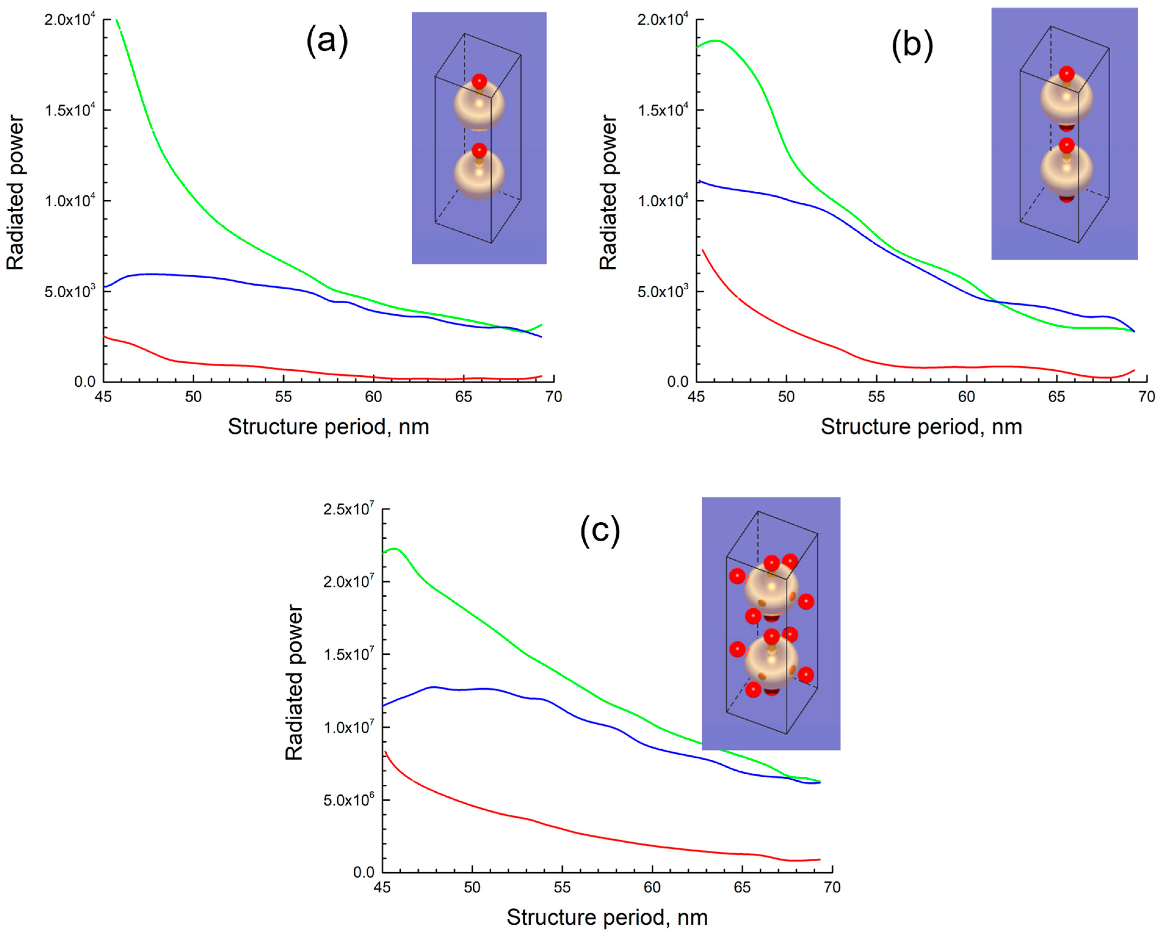
In the considered numerical model, one or several dipole emitters are located near each plasmonic nanoparticle (Figure 3) simulating SERS analyte molecules. The normalized power (8) emitted by a structure of ordered layers of spherical nanoparticles was calculated for different numbers of layers and spatial distributions of emitters. The radiation from the dipoles was averaged over three spatial orientations. As the calculation showed, the structural factor (i.e., specific spatial distribution of emitters), due to the smallness of the characteristic distances between emitters compared to the wavelength, had a minor effect on the integral characteristics of the radiation, which leads to similar qualitative patterns of radiation of the emitters system in the case of different numbers (Figure 3a–c). Therefore, one emitter near each nanoparticle structure without a loss of generality was adopted as a working model (Figure 3a).
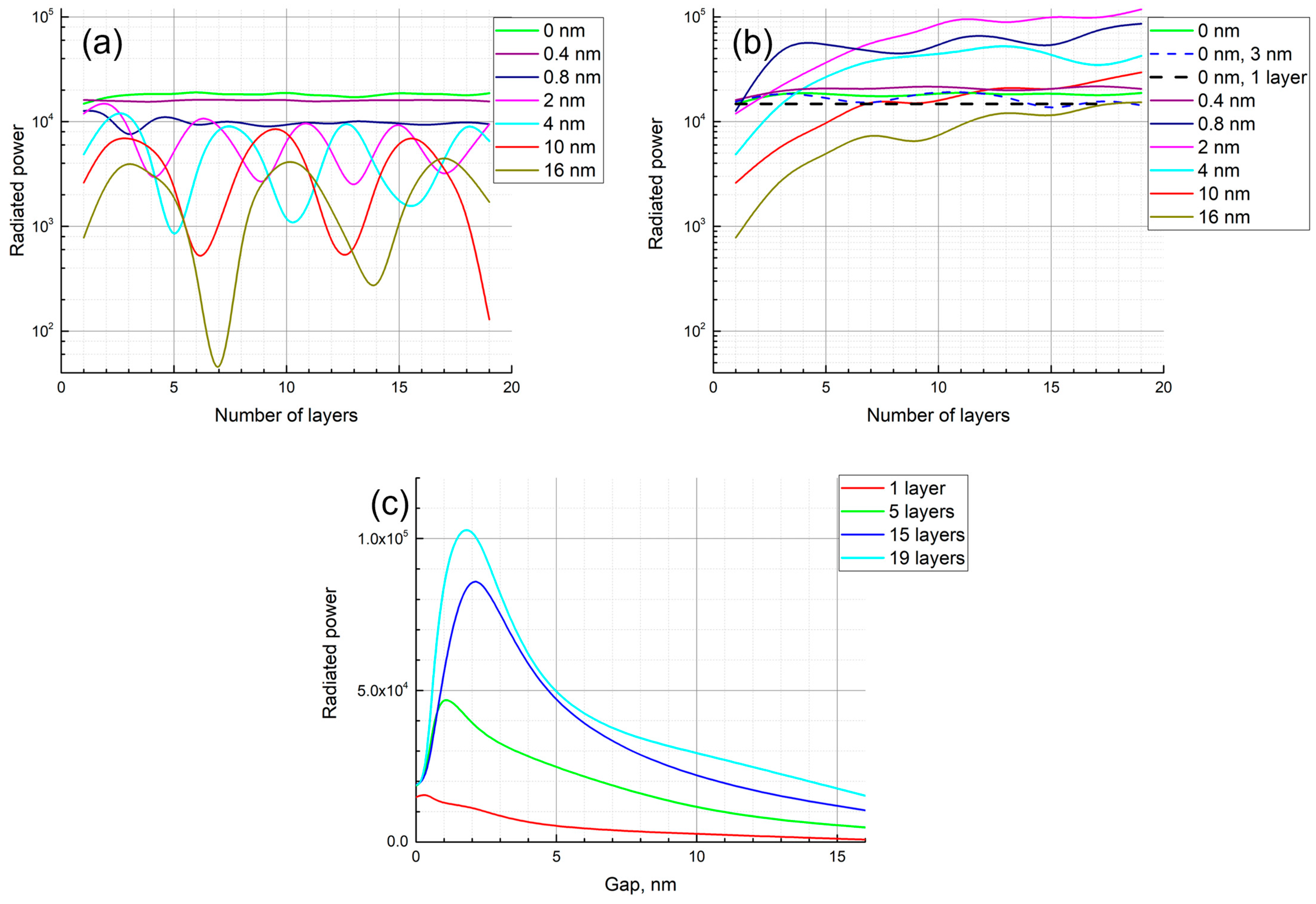
Initially, for the simplicity of the model, the phase of all emitters was assumed to be the same, i.e., the emitters were coherent. The calculation in this case showed (Figure 4a) that there was a periodic dependence of the emitted power on the number of layers of the structure. The first maximum occurred when the structure thickness was 4–6 layers, depending on the gap between nanoparticles in the (xy) plane. The observed periodicity indicates the interference nature of the radiation occurring within the structure, and it is associated with the actual coherence of the emitters. In order to simulate real incoherent emitters, each emitter was further given a random phase, and then the averaging over the ensemble was performed. In the case of incoherent emitters, a clearly visible saturation can be seen in Figure 4b, while some periodicity of small amplitude is still present. It should be noted that up to a structure thickness of 5–7 layers, the dependences for coherent and incoherent emitters (Figure 4a,b) are close to each other. This happens because the emitter closest to the surface mainly contributes to the radiation registered in the far zone, while the “background” from the remaining (coherent or incoherent) emitters is not too significant due to the rapid attenuation of electromagnetic radiation by absorbing plasmonic nanoparticles. This absorption leads to a clearly visible saturation for both coherent and non-coherent emitters (green lines in Figure 4a,b) when the structure period coincides with the nanoparticle diameter (i.e., nanoparticles are in contact). In ref. [33], for a densely packed structure of gold octahedra, a similar saturation of radiation is noted; as the number of layers of the structure increases to more than 4–5, the emitted power registered in the far zone ceases to increase.
The calculated power emitted by the multilayer SERS structure with gaps between nanoparticles measuring close to several nanometers can significantly exceed the power emitted by the SERS structure in the form of a monolayer of nanoparticles. Increasing the number of layers with a distance between plasmonic nanoparticles of more than several nanometers leads only to a partial absorption of emitted radiation. It leads to the appearance of a periodic interference pattern in the case of coherent emitters (red lines in Figure 4a) or to a monotonic increase of the radiated power for incoherent ones.
The calculated dependence of the emitted power by the gap between nanoparticles (Figure 4c) has a clearly expressed maximum for multilayer structures at a gap equal to 2 nm; with larger gaps, the emitted power decreases by an order of magnitude, remaining proportional to the number of layers. Thus, the spatial structure of nanoparticles deposited on a 3D CNT substrate has the property of scalability relative to the thickness of the structure. The lateral gaps between nanoparticles in a multilayer structure serve as effective channels that guide radiation from the underlying layers.
For the same reason, emitters located in a gap make a significantly larger contribution to the integral radiation compared to those located above and below a nanoparticle. Thus, in the configurations presented in Figure 3a,b, the emitted power is almost the same, while the number of emitters in these configurations differs twice; at the same time, adding a small number of emitters into the lateral gap between the nanoparticles increases the emitted power by three orders of magnitude.
Thus, in a sparse spatial structure of plasmonic nanoparticles, despite inevitable intrinsic self-absorption in this structure, it is possible to obtain a SERS signal (involving a higher number of nanoparticles) that exceeds that obtained from a densely packed monolayer of nanoparticles (black dotted line in Figure 4b) and makes such structures promising SERS substrates.

4. Discussion: CNT Arrays as a 3D Substrate for Plasmonic Nanoparticles

The aim of this work is to study the possibility of scaling the SERS signal using three-dimensional SERS substrates. A numerical calculation was performed for the configuration shown in Figure 2. This configuration was used, for example, in the work [30]. The calculation shows that, at least for the parameters used, the SERS substrate represented by the CNT array does not have a significant influence on the calculated integral optic signal in the far zone. A similar result (low influence of the CNT substrate) is experimentally obtained in work [32] for silver nanoparticles deposited on a substrate formed by the «grating» of carbon nanotubes. Thus, a 3D CNT substrate in quite an arbitrary configuration is promising for creating sparse plasmonic 3D structures. The use of the Purcell factor allows for the optimization of 3D structures from plasmonic nanoparticles with quite an arbitrary geometry, similar, for example, to those obtained in refs. [15,32], which cannot be done using a commonly used local field criterion [16,25,26,27,28,29].
Numerical calculations demonstrated that in the case of a sparse arrangement of plasmonic nanoparticles, it was possible to avoid the saturation of the SERS signal that was noted for the dense 3D arrays of plasmonic nanoparticles considered in refs. [32,33]. It is shown that a three-dimensional SERS substrate allows one to achieve a significant improvement in the signal compared to a two-dimensional one.
The performed numerical calculation allows us to determine the general concept and direction of further experimental research. Based on the obtained numerical results, it is possible to propose as a 3D SERS substrate a simple structure in the form of a CNT forest decorated with plasmonic nanoparticles [30,46,47,48] and to focus on optimizing its geometric parameters. Experimental and theoretical works in this direction, as well as a comparison of numerical results with experimental ones, are planned for future work.

5. Conclusions

This paper theoretically shows that for SERS structures, the Purcell factor, which takes into account the impact of the microscopic structure on the optical response of the system, is a more suitable optimization criterion than the widely used local field enhancement. The numerical technique of 3D SERS substrate optimization using the finite element method is proposed. It is shown that the method is capable of representing the direct calculation of the optical response of the optimized system in the far zone. Numerical simulations of the model demonstrate that in a sparse spatial structure of plasmonic nanoparticles, it is possible to obtain a SERS signal exceeding the one emitted by a densely packed monolayer of nanoparticles. It is also shown that the signal of a SERS substrate based on a three-dimensional CNT structure can be scalable by increasing the number of layers.

Author Contributions

Conceptualization, A.K. and E.K.; software, A.K.; investigation, A.K., E.K. and A.S.; resources, E.K.; writing—original draft preparation, A.K., A.S., E.K. and D.K.; writing—review and editing, A.K.; supervision, E.K.; funding acquisition, E.K. All authors have read and agreed to the published version of the manuscript.

Funding

The results of Section 1 and Section 2 are obtained within the state assignment of the Ministry of Science and Higher Education of the Russian Federation (Megagrant program, #075-15-2021-581). The results of Section 3 and Section 4 (related to numerical modelling of 3D SERS substrates) are obtained within the state assignment of the Ministry of Science and Higher Education of the Russian Federation (project FNRM-2021-0002). The method of numerical calculation of local fields using finite element method in a dense array of carbon nanotubes was developed with the support of the RSF grant (#23-19-00880).

Institutional Review Board Statement

Not applicable.

Informed Consent Statement

Not applicable.

Data Availability Statement

The data presented in this study are available on request from the corresponding author.

Conflicts of Interest

The authors declare no conflicts of interest.

References

  1. Phan-Quang, G.C.; Han, X.; Koh, C.S.L.; Sim, H.Y.F.; Lay, C.L.; Leong, S.X.; Lee, Y.H.; Pazos-Perez, N.; Alvarez-Puebla, R.A.; Ling, X.Y. Three-Dimensional Surface-Enhanced Raman Scattering Platforms: Large-Scale Plasmonic Hotspots for New Applications in Sensing, Microreaction, and Data Storage. Acc. Chem. Res. 2019, 52, 1844–1854. [Google Scholar] [CrossRef] [PubMed]
  2. Bondarev, I.V.; Gulyuk, A.V. Electromagnetic SERS Effect in Carbon Nanotube Systems. Superlattices Microstruct. 2015, 87, 103–108. [Google Scholar] [CrossRef]
  3. Bharati, M.S.S.; Soma, V.R. Flexible SERS Substrates for Hazardous Materials Detection: Recent Advances. Opto-Electron. Adv. 2021, 4, 210048. [Google Scholar] [CrossRef]
  4. Novotny, L.; van Hulst, N. Antennas for Light. Nat. Photonics 2011, 5, 83–90. [Google Scholar] [CrossRef]
  5. Sauvan, C.; Hugonin, J.P.; Maksymov, I.S.; Lalanne, P. Theory of the Spontaneous Optical Emission of Nanosize Photonic and Plasmon Resonators. Phys. Rev. Lett. 2013, 110, 237401. [Google Scholar] [CrossRef] [PubMed]
  6. Greffet, J.-J. Applied Physics. Nanoantennas for Light Emission. Science 2005, 308, 1561–1563. [Google Scholar] [CrossRef] [PubMed]
  7. Kuznetsov, A.V.; Valero, A.C.; Tarkhov, M.; Bobrovs, V.; Redka, D.; Shalin, A.S. Transparent Hybrid Anapole Metasurfaces with Negligible Electromagnetic Coupling for Phase Engineering. Nanophotonics 2021, 10, 4385–4398. [Google Scholar] [CrossRef]
  8. Terekhov, P.D.; Evlyukhin, A.B.; Shalin, A.S.; Karabchevsky, A. Polarization-Dependent Asymmetric Light Scattering by Silicon Nanopyramids and Their Multipoles Resonances. J. Appl. Phys. 2019, 125, 173108. [Google Scholar] [CrossRef]
  9. Kucherik, A.; Kutrovskaya, S.; Osipov, A.; Gerke, M.; Chestnov, I.; Arakelian, S.; Shalin, A.S.; Evlyukhin, A.B.; Kavokin, A.V. Nano-Antennas Based on Silicon-Gold Nanostructures. Sci. Rep. 2019, 9, 338. [Google Scholar] [CrossRef]
  10. Ginzburg, P. Cavity Quantum Electrodynamics in Application to Plasmonics and Metamaterials. Rev. Phys. 2016, 1, 120–139. [Google Scholar] [CrossRef]
  11. Ginzburg, P. Accelerating Spontaneous Emission in Open Resonators. Ann. Phys. 2016, 528, 571–579. [Google Scholar] [CrossRef]
  12. Novotny, L.; Hecht, B. Principles of Nano-Optics, 2nd ed.; Cambridge University Press: Cambridge, UK, 2012. [Google Scholar]
  13. Lai, R.; Chen, H.; Zhou, Z.; Yi, Z.; Tang, B.; Chen, J.; Yi, Y.; Tang, C.; Zhang, J.; Sun, T. Design of a Penta-Band Graphene-Based Terahertz Metamaterial Absorber with Fine Sensing Performance. Micromachines 2023, 14, 1802. [Google Scholar] [CrossRef] [PubMed]
  14. Lu, W.; Yi, Z.; Zhang, J.; Xu, X.; Tang, B.; Li, G.; Zeng, L.; Chen, J.; Sun, T. A Tunable Broadband Absorber in the Terahertz Band Based on the Proportional Structure of a Single Layer of Graphene. Diam. Relat. Mater. 2023, 140, 110481. [Google Scholar] [CrossRef]
  15. Zhao, X.; Yu, J.; Zhang, C.; Chen, C.; Xu, S.; Li, C.; Li, Z.; Zhang, S.; Liu, A.; Man, B. Flexible and Stretchable SERS Substrate Based on a Pyramidal PMMA Structure Hybridized with Graphene Oxide Passivated AgNPs. Appl. Surf. Sci. 2018, 455, 1171–1178. [Google Scholar] [CrossRef]
  16. Solís, D.M.; Taboada, J.M.; Obelleiro, F.; Liz-Marzán, L.M.; García De Abajo, F.J. Optimization of Nanoparticle-Based SERS Substrates through Large-Scale Realistic Simulations. ACS Photonics 2017, 4, 329–337. [Google Scholar] [CrossRef] [PubMed]
  17. Maier, S.A. Plasmonic Field Enhancement and SERS in the Effective Mode Volume Picture. Opt. Express 2006, 14, 1957. [Google Scholar] [CrossRef] [PubMed]
  18. Yang, X.; Zhou, Z.; Qi, J.; Zhang, S.; Guo, K.; Zhao, S. Modeling and Theoretical Analysis of the SERS Enhancement Factor Considering the Electronic Structural Energy. IEEE Access 2021, 9, 121279–121287. [Google Scholar] [CrossRef]
  19. Kadochkin, A.S.; Shalin, A.S.; Ginzburg, P. Granular Permittivity Representation in Extremely Near-Field Light-Matter Interaction Processes. ACS Photonics 2017, 4, 2137–2143. [Google Scholar] [CrossRef]
  20. Neuman, T.; Aizpurua, J.; Esteban, R. Quantum Theory of Surface-Enhanced Resonant Raman Scattering (SERRS) of Molecules in Strongly Coupled Plasmon-Exciton Systems. Nanophotonics 2020, 9, 295–308. [Google Scholar] [CrossRef]
  21. Liang, X.; Li, N.; Zhang, R.; Yin, P.; Zhang, C.; Yang, N.; Liang, K.; Kong, B. Carbon-Based SERS Biosensor: From Substrate Design to Sensing and Bioapplication. NPG Asia Mater. 2021, 13, 8. [Google Scholar] [CrossRef]
  22. Visaveliya, N.R.; Mazetyte-Stasinskiene, R.; Köhler, J.M. General Background of SERS Sensing and Perspectives on Polymer-Supported Plasmon-Active Multiscale and Hierarchical Sensor Particles. Adv. Opt. Mater. 2022, 10, 2102001. [Google Scholar] [CrossRef]
  23. Vo-Dinh, T. SERS Chemical Sensors and Biosensors: New Tools for Environmental and Biological Analysis. Sens. Actuators B 1995, 29, 189. [Google Scholar] [CrossRef]
  24. Shi, R.; Liu, X.; Ying, Y. Facing Challenges in Real-Life Application of Surface-Enhanced Raman Scattering: Design and Nanofabrication of Surface-Enhanced Raman Scattering Substrates for Rapid Field Test of Food Contaminants. J. Agric. Food Chem. 2018, 66, 6525–6543. [Google Scholar] [CrossRef]
  25. Son, J.; Kim, G.-H.; Lee, Y.; Lee, C.; Cha, S.; Nam, J.-M. Toward Quantitative Surface-Enhanced Raman Scattering with Plasmonic Nanoparticles: Multiscale View on Heterogeneities in Particle Morphology, Surface Modification, Interface, and Analytical Protocols. J. Am. Chem. Soc. 2022, 144, 22337–22351. [Google Scholar] [CrossRef] [PubMed]
  26. Zha, Z.; Liu, R.; Yang, W.; Li, C.; Gao, J.; Shafi, M.; Fan, X.; Li, Z.; Du, X.; Jiang, S. Surface-Enhanced Raman Scattering by the Composite Structure of Ag NP-Multilayer Au Films Separated by Al2O3. Opt. Express 2021, 29, 8890. [Google Scholar] [CrossRef] [PubMed]
  27. Yan, B.X.; Zhu, Y.Y.; Wei, Y.; Pei, H. Study on Surface Enhanced Raman Scattering of Au and Au@Al2O3 Spherical Dimers Based on 3D Finite Element Method. Sci. Rep. 2021, 11, 8391. [Google Scholar] [CrossRef]
  28. Yan, C.-C.; Che, Z.-L.; Yang, W.-Y.; Wang, X.-D.; Liao, L.-S. Deep-Red and near-Infrared Organic Lasers Based on Centrosymmetric Molecules with Excited-State Intramolecular Double Proton Transfer Activity. Opto-Electron. Adv. 2023, 6, 230007. [Google Scholar] [CrossRef]
  29. Stockman, M.I. Electromagnetic Theory of SERS. In Surface-Enhanced Raman Scattering—Physics and Applications; Kneipp, K., Moscovits, M., Kneipp, H., Eds.; Springer: Berlin/Heidelberg, Germany, 2006; pp. 47–65. [Google Scholar]
  30. Lee, S.; Hahm, M.G.; Vajtai, R.; Hashim, D.P.; Thurakitseree, T.; Chipara, A.C.; Ajayan, P.M.; Hafner, J.H. Utilizing 3D SERS Active Volumes in Aligned Carbon Nanotube Scaffold Substrates. Adv. Mater. 2012, 24, 5261–5266. [Google Scholar] [CrossRef]
  31. Lee, M.K.; Seo, J.; Cho, S.J.; Jo, Y.; Kim, S.; Kang, Y.; Lee, H. Novel 3D Arrays of Gold Nanostructures on Suspended Platinum-Coated Carbon Nanotubes as Surface-Enhanced Raman Scattering Substrates. Mater. Lett. 2012, 81, 9–12. [Google Scholar] [CrossRef]
  32. Sun, Y.; Liu, K.; Miao, J.; Wang, Z.; Tian, B.; Zhang, L.; Li, Q.; Fan, S.; Jiang, K. Highly Sensitive Surface-Enhanced Raman Scattering Substrate Made from Superaligned Carbon Nanotubes. Nano Lett. 2010, 10, 1747–1753. [Google Scholar] [CrossRef]
  33. Han, Y.; Wu, S.R.; Tian, X.D.; Zhang, Y. Optimizing the SERS Performance of 3D Substrates through Tunable 3D Plasmonic Coupling toward Label-Free Liver Cancer Cell Classification. ACS Appl. Mater. Interfaces 2020, 12, 28965–28974. [Google Scholar] [CrossRef] [PubMed]
  34. Maslovski, S.I.; Simovski, C.R. Purcell Factor and Local Intensity Enhancement in Surface-Enhanced Raman Scattering. Nanophotonics 2019, 8, 429–434. [Google Scholar] [CrossRef]
  35. Born, M.; Wolf, E. Principles of Optics: Electromagnetic Theory of Propagation, Interference and Diffraction of Light, 7th ed.; Cambridge University Press: Cambridge, UK, 1999; ISBN 0-521-64222-1. [Google Scholar]
  36. Falkovsky, L.A. Optical Properties of Graphene and IV–VI Semiconductors. Uspekhi Fiz. Nauk. 2008, 178, 923. [Google Scholar] [CrossRef]
  37. Kadochkin, A.S.; Moiseev, S.G.; Svetukhin, V.V.; Saurov, A.N.; Zolotovskii, I.O. Excitation of Ultraslow High-q Surface Plasmon Polariton Modes in Dense Arrays of Double-Walled Carbon Nanotubes. Ann. Phys. 2022, 534, 2100438. [Google Scholar] [CrossRef]
  38. Kildishev, A.V. Graphene Paves the Way for Next-Generation Plasmonics. Available online: https://www.comsol.com/story/graphene-paves-the-way-for-next-generation-plasmonics-53551 (accessed on 25 December 2023).
  39. Martín-Moreno, L.; De Abajo, F.J.G.; García-Vidal, F.J. Ultraefficient Coupling of a Quantum Emitter to the Tunable Guided Plasmons of a Carbon Nanotube. Phys. Rev. Lett. 2015, 115, 173601. [Google Scholar] [CrossRef]
  40. Kadochkin, A.S.; Moiseev, S.; Dadoenkova, Y.S.; Bentivegna, F.; Svetukhin, V.; Zolotovsky, I.O. Resonant Amplification of Surface Plasmon Polaritons with an Electric Current in a Single-Walled Carbon Nanotube Lying on a Spatially Modulated Substrate. J. Opt. 2020, 22, 125002. [Google Scholar] [CrossRef]
  41. Falkovsky, L.A.; Pershoguba, S.S. Optical Far-Infrared Properties of a Graphene Monolayer and Multilayer. Phys. Rev. B Condens. Matter Mater. Phys. 2007, 76, 153410. [Google Scholar] [CrossRef]
  42. Yu, P.; Fesenko, V.I.; Tuz, V.R. Dispersion Features of Complex Waves in a Graphene-Coated Semiconductor Nanowire. Nanophotonics 2018, 7, 925–934. [Google Scholar] [CrossRef]
  43. Nikitin, A.Y.; Guinea, F.; García-Vidal, F.J.; Martín-Moreno, L. Edge and Waveguide Terahertz Surface Plasmon Modes in Graphene Microribbons. Phys. Rev. B Condens. Matter Mater. Phys. 2011, 84, 161407. [Google Scholar] [CrossRef]
  44. Hajaj, E.M.; Shtempluk, O.; Kochetkov, V.; Razin, A.; Yaish, Y.E. Chemical Potential of Inhomogeneous Single-Layer Graphene. Phys. Rev. B Condens. Matter Mater. Phys. 2013, 88, 045128. [Google Scholar] [CrossRef]
  45. De Abajo, F.J.G. Graphene Plasmonics: Challenges and Opportunities. ACS Photonics 2014, 1, 133–152. [Google Scholar] [CrossRef]
  46. Szabó, A.; Bakos, L.P.; Karajz, D.; Gyulavári, T.; Tóth, Z.-R.; Pap, Z.; Szilágyi, I.M.; Igricz, T.; Parditka, B.; Erdélyi, Z.; et al. Decoration of Vertically Aligned Carbon Nanotubes with Semiconductor Nanoparticles Using Atomic Layer Deposition. Materials 2019, 12, 1095. [Google Scholar] [CrossRef] [PubMed]
  47. Janas, D.; Koziol, K.K.K. The Influence of Metal Nanoparticles on Electrical Properties of Carbon Nanotubes. Appl. Surf. Sci. 2016, 376, 74–78. [Google Scholar] [CrossRef]
  48. Olivares, F.; Peón, F.; Henríquez, R.; del Río, R.S. Strategies for Area-Selective Deposition of Metal Nanoparticles on Carbon Nanotubes and Their Applications: A Review. J. Mater. Sci. 2022, 57, 2362–2387. [Google Scholar] [CrossRef]
Figure 1. (a) Field enhancement and (b) antenna effect. Here, d 1 is the SERS molecule near the nanoparticle, and d 2 is the dipole “modeling” the incident wave.
Photonics 11 00012 g001
Figure 2. 3D SERS substrate. (a) Numerical model; (b) sketch of experimental sample design. Abbreviations are defined in the main text. Diameter of silver nanoparticle is equal to 40 nm, and diameter of the modelled CNT is equal to 5 nm.
Photonics 11 00012 g002
Figure 3. Influence of structural factor on radiated power. The insets show the number and location of emitters (small red spheres on the insets) near the plasmonic nanosphere (metallic sphere on the insets): (a) one emitter, (b) two emitters, (c) six emitters. The colored lines correspond to the number of layers of nanoparticles: red line—1 layer, green line—4 layers, blue line—7 layers. The carbon nanotube is not shown. Dipole moment is equal to 9D, which corresponds to rhodamine R6G.
Photonics 11 00012 g003
Figure 4. Total radiated power (related to the cross-section of the unit cell, W/m2) for different numbers of SERS substrate layers; (a) radiated power depending on the period of the structure for different numbers of layers in the case of coherent emitters; (b) radiated power depending on the period of the structure for different numbers of layers in the case of incoherent (random) emitters; (c) radiated power depending on the gap between nanoparticles within a layer (see Figure 2a). Green lines in panels (a,b) correspond to the case where plasmonic nanoparticles are in contact in the (xy) plane. The interparticle distance in the z-direction is everywhere equal to one diameter of the nanoparticle, except for the blue dashed line in panel (b), where the interparticle distance is equal to 3 nm.
Photonics 11 00012 g004
Disclaimer/Publisher’s Note: The statements, opinions and data contained in all publications are solely those of the individual author(s) and contributor(s) and not of MDPI and/or the editor(s). MDPI and/or the editor(s) disclaim responsibility for any injury to people or property resulting from any ideas, methods, instructions or products referred to in the content.