Research on the Structure Design of Silicon Avalanche Photodiode with Near-Ultraviolet High Responsivity


 ,
,
Abstract
:1. Introduction
2. Design of Si-APD Structure
2.1. Analysis of the Basic Characteristics of Si-APD
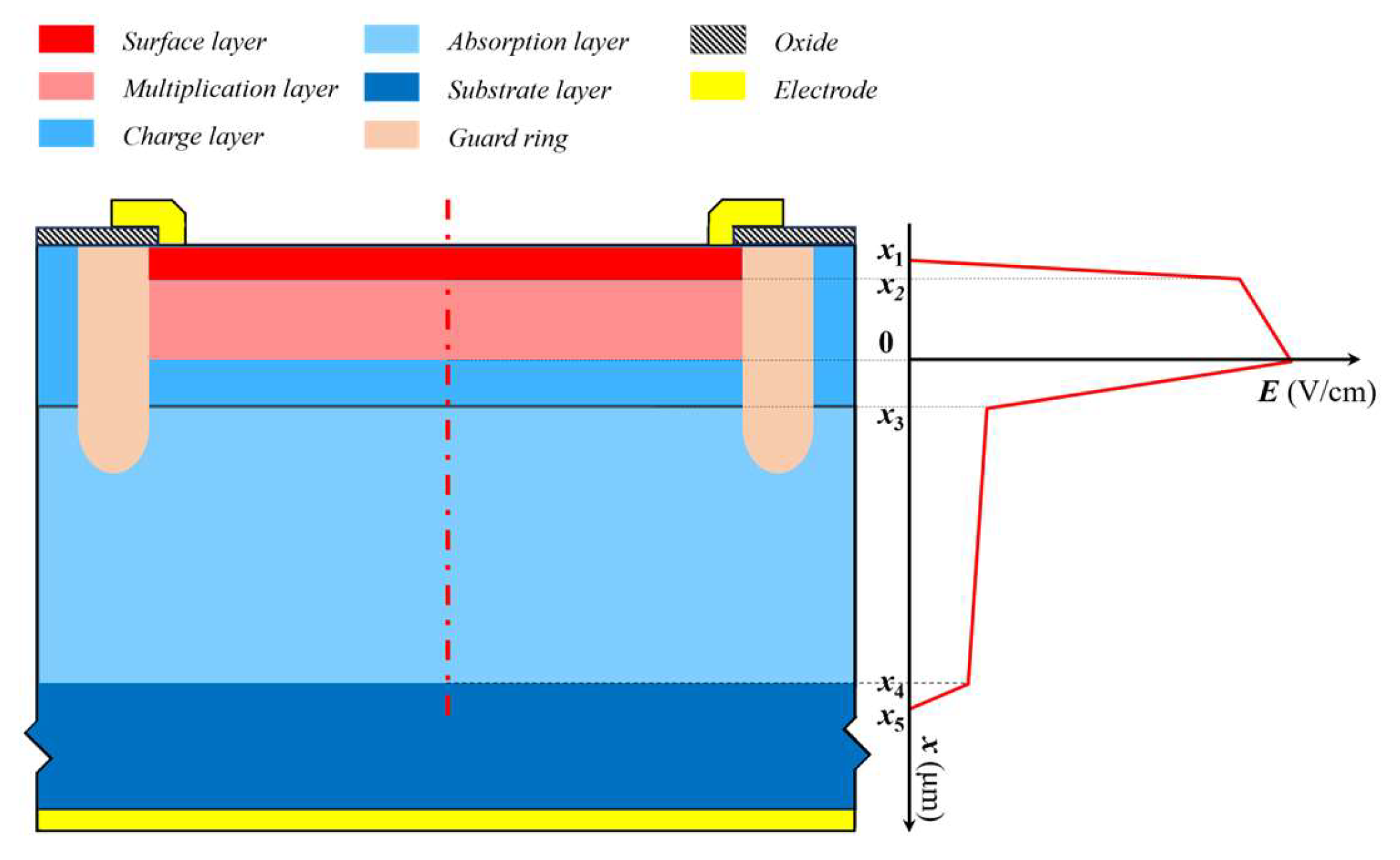
2.2. Design and Analysis of Si-APD Structure
3. Structural Optimization and Discussion of Results
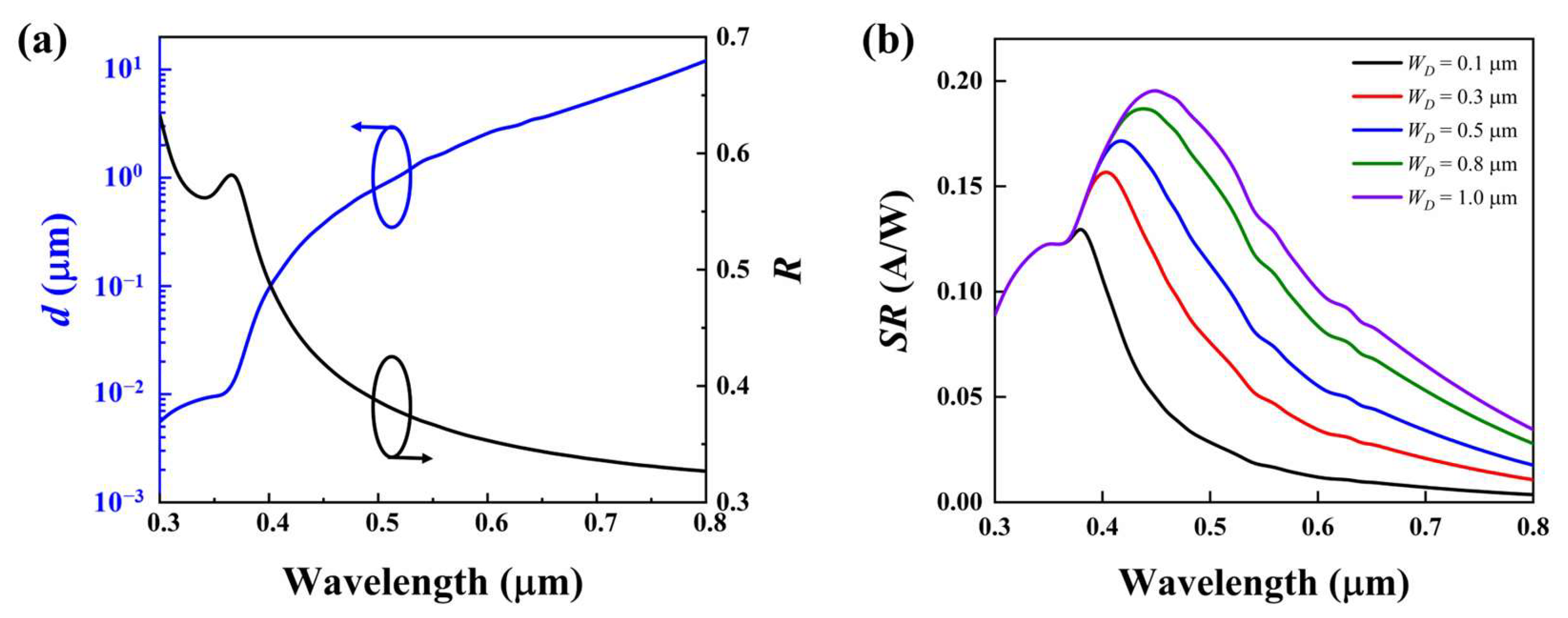
3.1. Electric Field Distribution and Responsivity of Si-APD
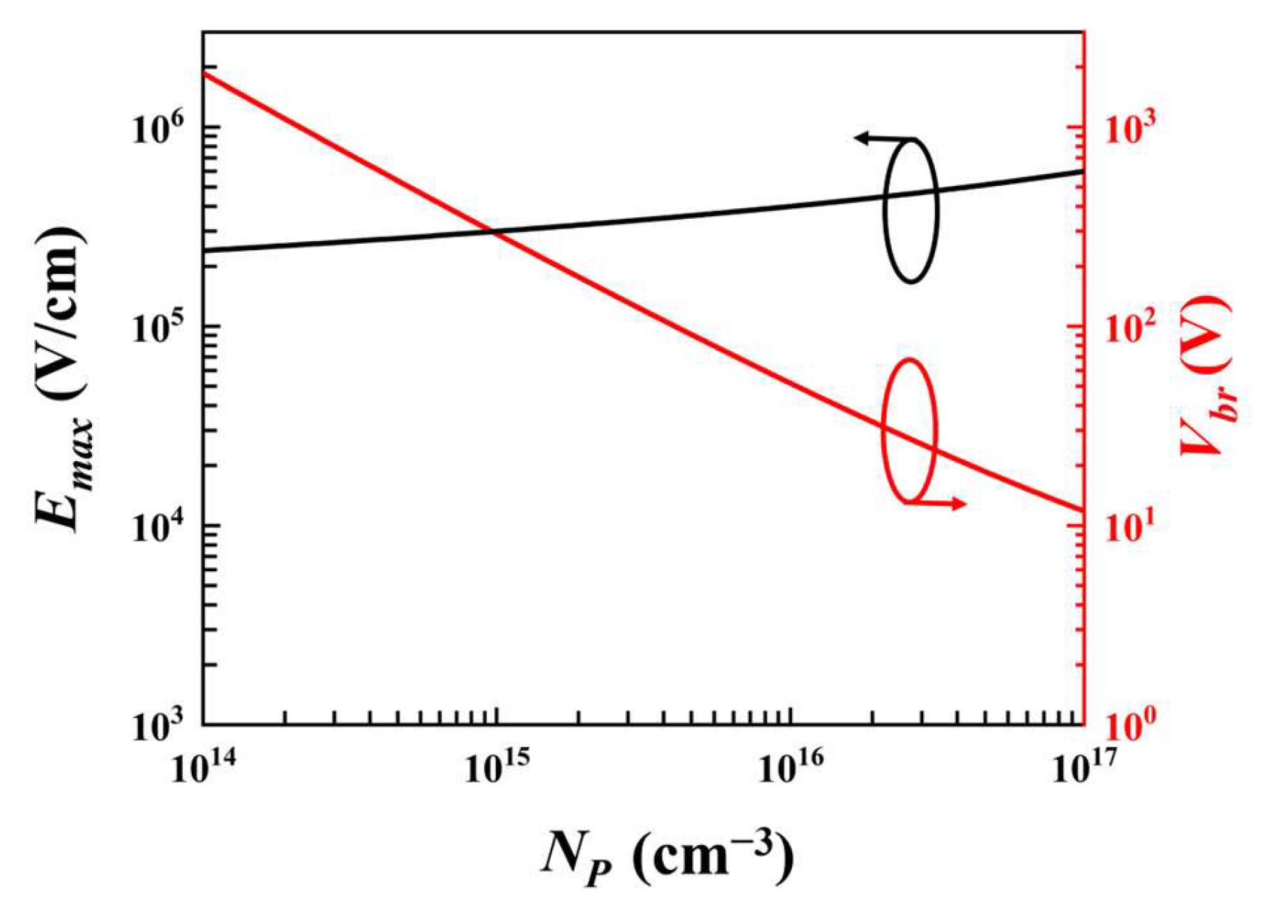
3.2. Optimization of Si-APD Structural Parameters
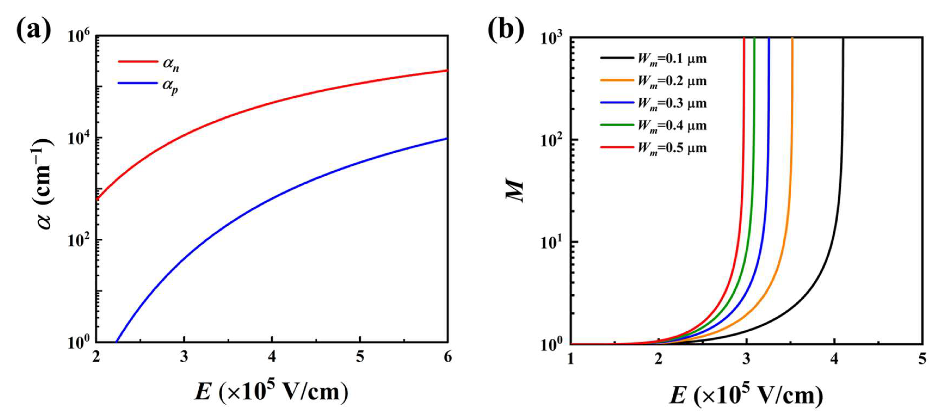
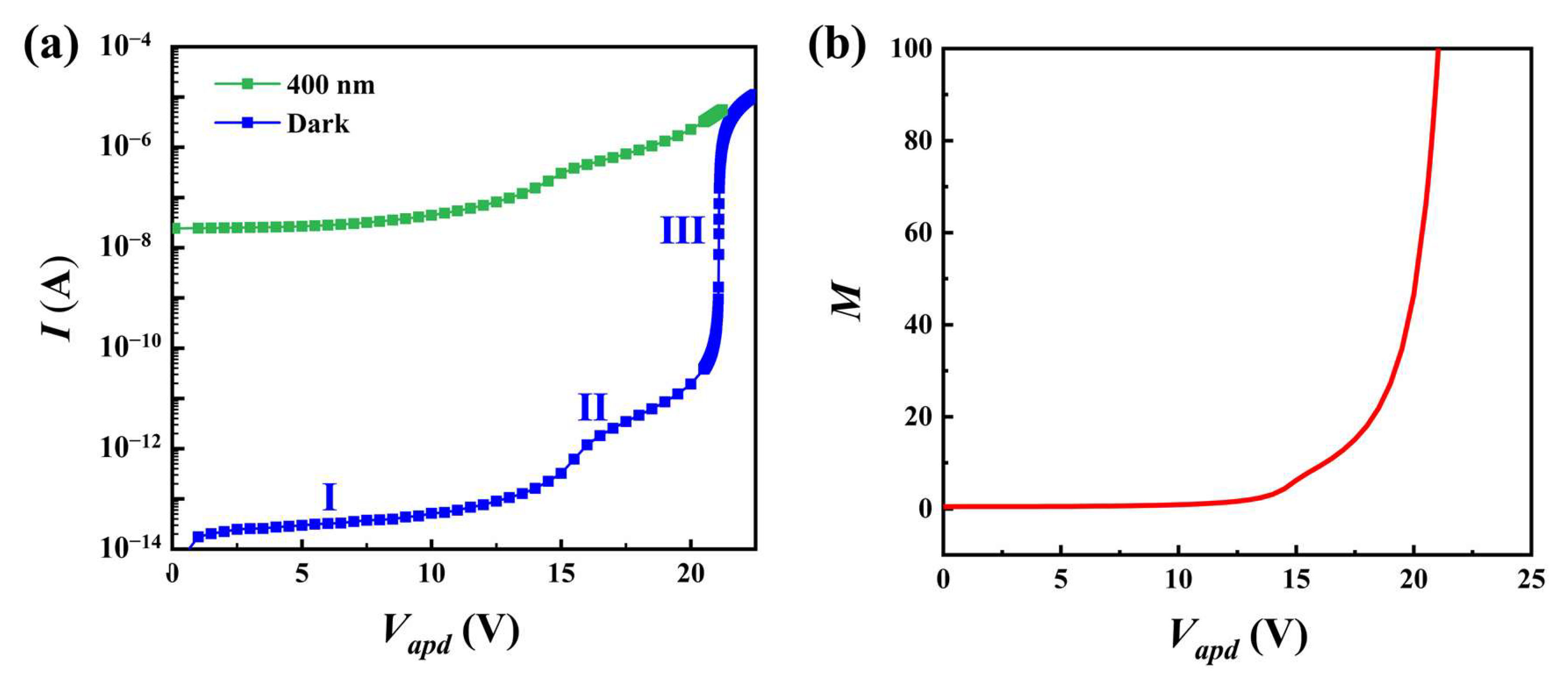
3.3. I-V and Avalanche Multiplication Characteristics of Si-APD
4. Conclusions
Author Contributions
Funding
Institutional Review Board Statement
Informed Consent Statement
Data Availability Statement
Conflicts of Interest
References
- Chen, J.; Ouyang, W.; Yang, W.; He, J.; Fang, X. Recent progress of heterojunction ultraviolet photodetectors: Materials, integrations, and applications. Adv. Funct. Mater. 2020, 30, 1909909. [Google Scholar] [CrossRef]
- Liang, F.; Chen, W.; Feng, M.; Huang, Y.; Liu, J.; Sun, X.; Zhan, X.; Sun, Q.; Wu, Q.; Yang, H. Effect of Si Doping on the Performance of GaN Schottky Barrier Ultraviolet Photodetector Grown on Si Substrate. Photonics 2021, 8, 28. [Google Scholar] [CrossRef]
- Liu, Q.; Xu, L.; Jin, Y.; Zhang, S.; Wang, Y.; Hu, A.; Guo, X. Ultraviolet Response in Coplanar Silicon Avalanche Photodiodes with CMOS Compatibility. Sensors 2022, 22, 3873. [Google Scholar] [CrossRef] [PubMed]
- Wang, J.; Xing, Y.; Wan, F.; Fu, C.; Xu, C.-H.; Liang, F.-X.; Luo, L.-B. Progress in ultraviolet photodetectors based on II–VI group compound semiconductors. J. Mater. Chem. C 2022, 10, 12929–12946. [Google Scholar] [CrossRef]
- Rogalski, A.; Bielecki, Z.; Mikołajczyk, J.; Wojtas, J. Ultraviolet Photodetectors: From Photocathodes to Low-Dimensional Solids. Sensors 2023, 23, 4452. [Google Scholar] [CrossRef] [PubMed]
- Shi, L.; Nihtianov, S. Comparative study of silicon-based ultraviolet photodetectors. IEEE Sens. J. 2012, 12, 2453–2459. [Google Scholar] [CrossRef]
- Lincke, R.; Wilkerson, T.D. New detector for the vacuum ultraviolet. Rev. Sci. Instrum. 1962, 33, 911–913. [Google Scholar] [CrossRef]
- Razeghi, M.; Rogalski, A. Semiconductor ultraviolet detectors. J. Appl. Phys. 1996, 79, 7433–7473. [Google Scholar] [CrossRef]
- Alaie, Z.; Nejad, S.M.; Yousefi, M.H. Recent advances in ultraviolet photodetectors. Mater. Sci. Semicond. Process. 2015, 29, 16–55. [Google Scholar] [CrossRef]
- Pauchard, A.; Besse, P.A.; Bartek, M.; Wolffenbuttel, R.; Popovic, R. Ultraviolet-selective avalanche photodiode. Sens. Actuators A Phys. 2000, 82, 128–134. [Google Scholar] [CrossRef]
- Shimotori, T.; Maekita, K.; Maruyama, T.; Iiyama, K. Characterization of APDs fabricated by 0.18 μm CMOS process in blue wavelength region. In Proceedings of the 2012 17th Opto-Electronics and Communications Conference, Busan, Republic of Korea, 2–6 July 2012; IEEE: Piscataway, NJ, USA, 2012; pp. 509–510. [Google Scholar]
- Myers, R.A.; Farrell, R.; Riccardi, S.L.; McClish, M. UV-enhanced silicon avalanche photodiodes. In Proceedings of the SPIE Optical Components and Materials X, SPIE OPTO, San Francisco, CA, USA, 2–7 February 2013; SPIE: Bellingham, WA, USA, 2013; Volume 8621, pp. 339–349. [Google Scholar]
- Napiah, Z.A.F.M.; Hishiki, T.; Iiyama, K. Wavelength dependence of silicon avalanche photodiode fabricated by CMOS process. Opt. Laser Technol. 2017, 92, 193–197. [Google Scholar] [CrossRef]
- Xia, Z.; Zang, K.; Liu, D.; Zhou, M.; Kim, T.-J.; Zhang, H.; Xue, M.; Park, J.; Morea, M.; Ryu, J.H.; et al. High-sensitivity silicon ultraviolet p+-in avalanche photodiode using ultra-shallow boron gradient doping. Appl. Phys. Lett. 2017, 111, 081109. [Google Scholar] [CrossRef]
- Iiyama, K.; Maruyama, T.; Gyobu, R.; Hishiki, T.; Shimotori, T. High speed and high responsivity avalanche photodiode fabricated by standard CMOS process in blue wavelength region. IEICE Trans. Electron. 2018, 101, 574–580. [Google Scholar] [CrossRef]
- Chen, W.S.; Wang, H.B.; Tao, J.; Gao, D.; Lv, J.G.; Qin, Y.X.; Guo, G.T.; Li, X.T.; Wang, Q.; Zhang, J.; et al. A study on the epitaxial structure and characteristics of high-efficiency blue silicon photodetectors. Chin. Opt. 2022, 15, 568–591. [Google Scholar]
- Xu, H.; Yang, Y.; Tan, J.; Chen, L.; Zhu, H.; Sun, Q. High-Performance Lateral Avalanche Photodiode Based on Silicon-on-Insulator Structure. IEEE Electron Device Lett. 2022, 43, 1077–1080. [Google Scholar] [CrossRef]
- Saleh, B.E.A.; Teich, M.C. Fundamentals of Photonics; John Wiley & Sons: Hoboken, NJ, USA, 1991. [Google Scholar]
- Schinke, C.; Christian Peest, P.; Schmidt, J.; Brendel, R.; Bothe, K.; Vogt, M.R.; Kröger, I.; Winter, S.; Schirmacher, A.; Lim, S.; et al. Uncertainty analysis for the coefficient of band-to-band absorption of crystalline silicon. AIP Adv. 2015, 5, 067168. [Google Scholar] [CrossRef]
- Sze, S.M.; Li, Y.; Ng, K.K. Physics of Semiconductor Devices, 3rd ed.; Xi’an Jiaotong University Press: Xi’an, China, 2008. [Google Scholar]
- Woods, M.H.; Johnson, W.C.; Lampert, M.A. Use of a Schottky barrier to measure impact ionization coefficients in semiconductors. Solid-State Electron. 1973, 16, 381–394. [Google Scholar] [CrossRef]
- Fossum, J.G.; Mertens, R.P.; Lee, D.S.; Nijs, J. Carrier recombination and lifetime in highly doped silicon. Solid-State Electron. 1983, 26, 569–576. [Google Scholar] [CrossRef]
- Neamen, D. Semiconductor Physics and Devices, 4th ed.; Publishing House of Electronics Industry: Beijing, China, 2018. [Google Scholar]
- Hall, R.N. Electron-hole recombination in germanium. Phys. Rev. 1952, 87, 387. [Google Scholar] [CrossRef]
- Shockley, W.; Read, W.T., Jr. Statistics of the recombinations of holes and electrons. Phys. Rev. 1952, 87, 835. [Google Scholar] [CrossRef]
- Joyce, W.B.; Dixon, R.W. Analytic approximations for the Fermi energy of an ideal Fermi gas. Appl. Phys. Lett. 1977, 31, 354–356. [Google Scholar] [CrossRef]
- Yu, Z.; Dutton, R.W. SEDAN III: A Generalized Electronic Material Device Analysis Program; Stanford University Electronics Laboratories Technical Report; Stanford University: Stanford, CA, USA, 1985. [Google Scholar]
- Van Overstraeten, R.; De Man, H. Measurement of the ionization rates in diffused silicon p-n junctions. Solid-State Electron. 1970, 13, 583–608. [Google Scholar] [CrossRef]
- Selberherr, S. Analysis and Simulation of Semiconductor Devices; Springer: New York, NY, USA, 1984. [Google Scholar]
- Arora, N.D.; Hauser, J.R.; Roulston, D.J. Electron and hole mobilities in silicon as a function of concentration and temperature. IEEE Trans. Electron Devices 1982, 29, 292–295. [Google Scholar] [CrossRef]
- Caughey, D.M.; Thomas, R.E. Carrier mobilities in silicon empirically related to doping and field. Proc. IEEE 1967, 55, 2192–2193. [Google Scholar] [CrossRef]
- Forrest, S. Performance of InxGa1-xAsyP1-y photodiodes with dark current limited by diffusion, generation recombination, and tunneling. IEEE J. Quantum Electron. 1981, 17, 217–226. [Google Scholar] [CrossRef]


| Doping Type | Thickness/μm | Doping Concentration/cm−3 |
|---|---|---|
| p+ | 0.10 | 1.0 × 10¹⁸ |
| p | 0.20 | 2.0 × 10¹⁶ |
| n | 0.15 | 2.0 × 10¹⁷ |
| n− | 1.00 | 1.0 × 10¹⁴ |
| n++ | 20.00 | 1.0 × 10¹⁹ |
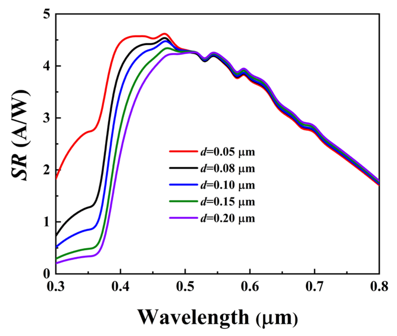
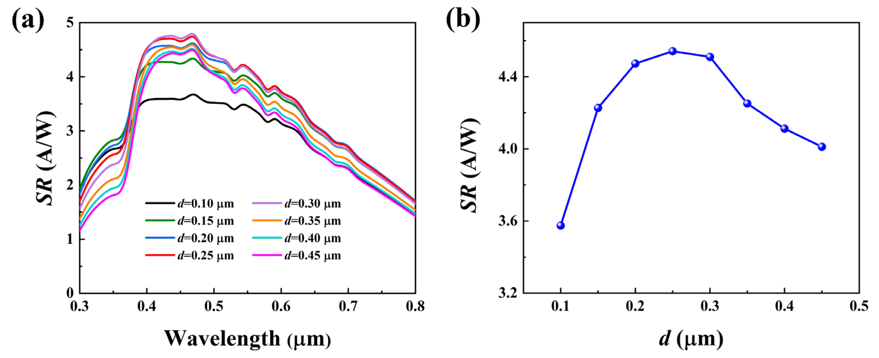
| d/μm | 0.10 | 0.15 | 0.20 | 0.25 | 0.30 | 0.35 | 0.40 | 0.45 |
| Vbr-apd/V | 26.53 | 23.60 | 21.87 | 21.12 | 21.01 | 21.36 | 22.08 | 23.00 |
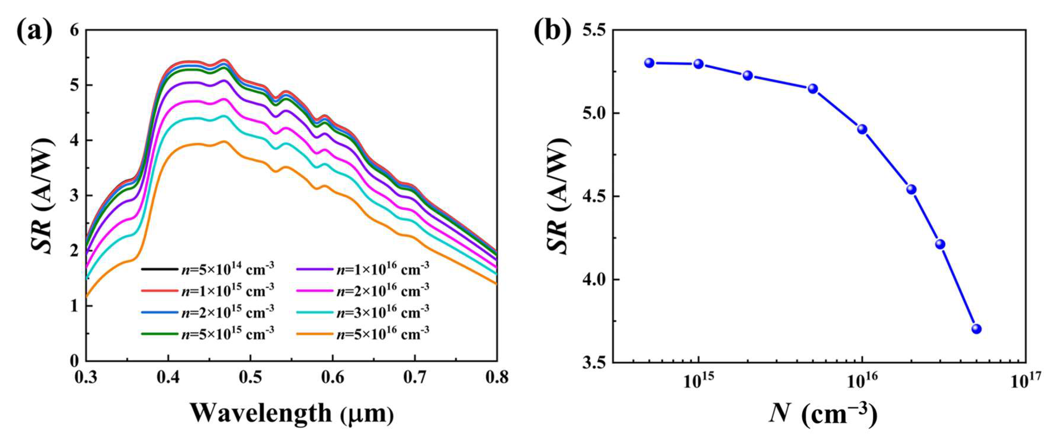
| N/cm−3 | 1 × 10¹⁵ | 2 × 10¹⁵ | 5 × 10¹⁵ | 8 × 10¹⁵ | 1 × 10¹⁶ | 2 × 10¹⁶ | 3 × 10¹⁶ | 5 × 10¹⁶ |
| Vbr-apd/V | 17.75 | 17.93 | 18.48 | 19.02 | 19.38 | 21.13 | 22.86 | 25.88 |
| N/cm−3 | 5 × 10¹³ | 1 × 10¹⁴ | 3 × 10¹⁴ | 1 × 10¹⁵ | 3 × 10¹⁵ | 5 × 10¹⁵ |
| Vbr-apd/V | 17.79 | 17.75 | 17.60 | 17.11 | 16.30 | 16.08 |
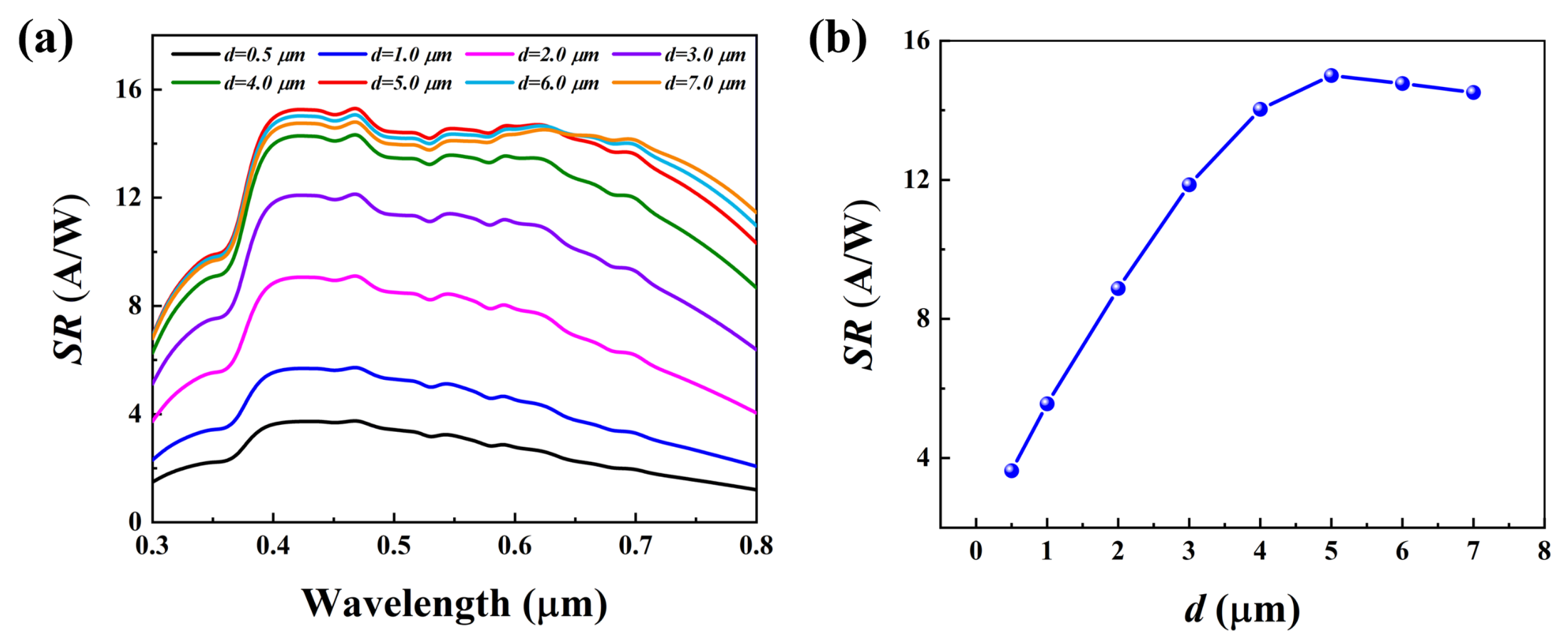
| d/μm | 0.5 | 1.0 | 2.0 | 3.0 | 4.0 | 5.0 | 6.0 | 7.0 |
| Vbr-apd/V | 16.71 | 17.60 | 19.16 | 20.23 | 20.85 | 21.07 | 21.09 | 21.09 |
| Doping Type | Thickness/μm | Doping Concentration/cm−3 |
|---|---|---|
| p+ | 0.05 | 1.0 × 10¹⁸ |
| p | 0.25 | 1.0 × 10¹⁵ |
| n | 0.15 | 2.0 × 10¹⁷ |
| n− | 5.00 | 3.0 × 10¹⁴ |
| n++ | 20.00 | 1.0 × 10¹⁹ |
Disclaimer/Publisher’s Note: The statements, opinions and data contained in all publications are solely those of the individual author(s) and contributor(s) and not of MDPI and/or the editor(s). MDPI and/or the editor(s) disclaim responsibility for any injury to people or property resulting from any ideas, methods, instructions or products referred to in the content. |
© 2023 by the authors. Licensee MDPI, Basel, Switzerland. This article is an open access article distributed under the terms and conditions of the Creative Commons Attribution (CC BY) license (https://creativecommons.org/licenses/by/4.0/).
Share and Cite
Guo, G.; Chen, W.; Zheng, K.; Lv, J.; Qin, Y.; Zhao, B.; Zhao, Y.; Chen, Y.; Gao, D.; Liang, J.; et al. Research on the Structure Design of Silicon Avalanche Photodiode with Near-Ultraviolet High Responsivity. Photonics 2024, 11, 1. https://doi.org/10.3390/photonics11010001
Guo G, Chen W, Zheng K, Lv J, Qin Y, Zhao B, Zhao Y, Chen Y, Gao D, Liang J, et al. Research on the Structure Design of Silicon Avalanche Photodiode with Near-Ultraviolet High Responsivity. Photonics. 2024; 11(1):1. https://doi.org/10.3390/photonics11010001
Chicago/Turabian StyleGuo, Guangtong, Weishuai Chen, Kaifeng Zheng, Jinguang Lv, Yuxin Qin, Baixuan Zhao, Yingze Zhao, Yupeng Chen, Dan Gao, Jingqiu Liang, and et al. 2024. "Research on the Structure Design of Silicon Avalanche Photodiode with Near-Ultraviolet High Responsivity" Photonics 11, no. 1: 1. https://doi.org/10.3390/photonics11010001
APA StyleGuo, G., Chen, W., Zheng, K., Lv, J., Qin, Y., Zhao, B., Zhao, Y., Chen, Y., Gao, D., Liang, J., & Wang, W. (2024). Research on the Structure Design of Silicon Avalanche Photodiode with Near-Ultraviolet High Responsivity. Photonics, 11(1), 1. https://doi.org/10.3390/photonics11010001