1. Introduction
Lithium niobate (
, LN) has been widely adopted in the development of electro-optic modulators due to its exceptional electro-optic coefficient, wide transmission window, and low optical loss within the telecom wavelengths [
1,
2]. Recently, thin-film LN modulators have emerged as promising solutions for next-generation low-voltage and high-bandwidth electro-optic applications. This is largely due to the improved voltage-bandwidth performance of thin-film LN modulators when compared to traditional LN platforms. In addition, thin-film LN modulators preserve essential advantages of LN materials such as linear response, absence of modulation-induced absorption, high optical power-handling ability, and low optical loss [
3,
4,
5]. The development of thin-film LN modulators has made rapid advancements, with the capability of achieving 100 GHz or higher speed rates [
6,
7].
However, as the modulator rates continue to increase, the thermal field within the device becomes increasingly significant [
8,
9]. As high-speed microwave (MW) and optical signals propagate through the device, energy loss is converted into heat, resulting in an increase in device temperature. This temperature rise affects the microwave and optical signals by altering the refractive index and conductivity of the material, as well as impacting the normal operation of other devices in the integrated system [
9,
10]. Therefore, it is essential to investigate the primary sources of heat generation, the temperature distribution within the device, and the resulting effects on the performance of LN modulators [
11].
In this work, we established a multi-physical simulation model based on the micro-structured electrode thin-film LN modulator published in [
12]. The model was used to investigate the heat generation sources, temperature distribution, and temperature effects on microwave and optical signals. Finally, we effectively improved the temperature rise and temperature distribution of the LN modulator by adding a diamond heat dissipation layer, which reduced the temperature’s impact on microwave and optical signals.
2. Multi-Physical Model of the LN Modulator
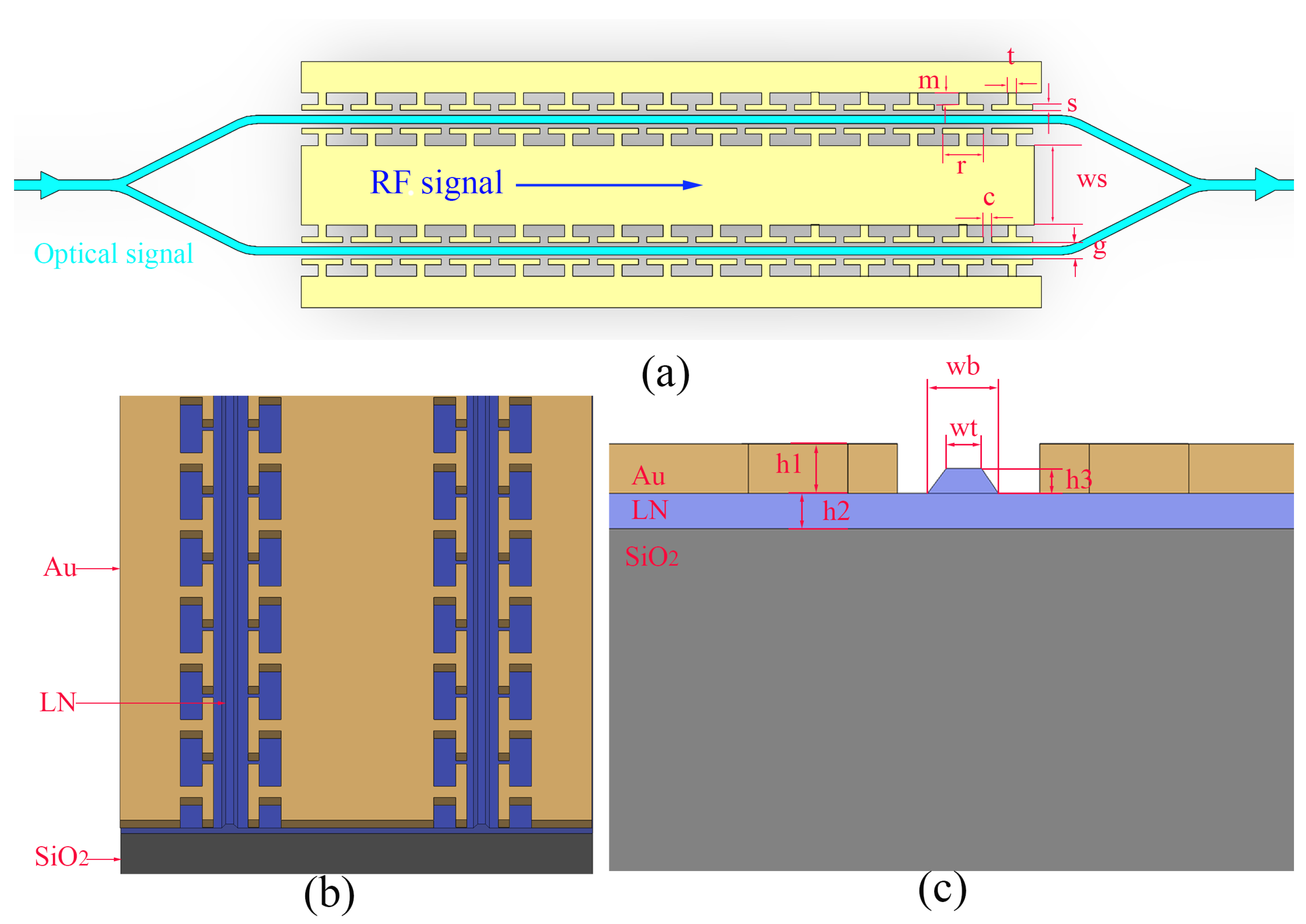
Figure 1 shows a 3D model of an LN modulator with T-shaped electrodes.This structure refers to that depicted in Ref. [
12]. In addition, most of the structural parameters are also taken from this study. The microwave effective refractive index needs to be as close as possible to the optical effective refractive index. However, the effective refractive index of a microwave is often smaller than the optical refractive index, and the speed of a microwave is faster than the speed of a light wave. Therefore, various slow wave electrode structures, such as T-shaped electrodes, have emerged. The bandwidth of the lithium niobate modulator is quite high, reaching 100 GHz or higher, which is sufficient for ethical use. Additionally, the slow wave effect is very apparent and the modulation efficiency is high. However, as previously mentioned, the temperature field becomes significant at higher frequencies, and we did not explore the temperature characteristics of the modulator. Therefore, this model was chosen as the basis for multi-physics simulation research.
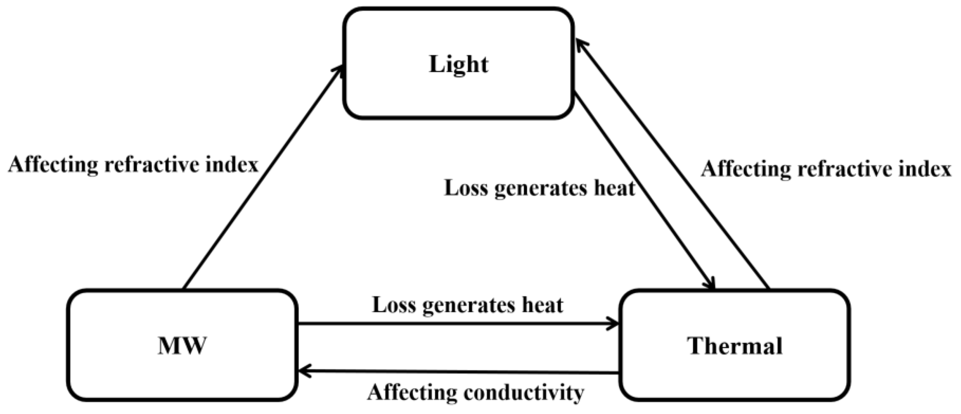
The relationships between different physical fields in thin-film LN modulators can be represented by
Figure 2. The transmitted optical and MW field are solved by the Helmholtz equation for E-field, which is part of Maxwell’s equation in frequency domain:
where
is the relative permittivity,
is the relative permeability,
is conductivity,
is wave vector in vacuum, and
is the MW frequency. For the elaboration of temperature profile, the generalized heating transfer differential equation is employed:
where
k is the thermal conductivity of the material,
is the specific heating,
is the density, and
Q is the heating generation rate.
The loss of optical and microwave signals during transmission produces heat and causes a temperature rise in the device. Therefore, it is only necessary to solve Equations (1) and (2) to obtain the losses of the optical and microwave signals and then substitute them into Equation (
3) to calculate the temperature rise of the LN modulator. This article uses two methods to perform these calculations, both of which were realized using mature simulation software on the market. One is the joint simulation of HFSS and Icepak, and the other is the use of Comsol Multiphysics simulation software.
On the other hand, both the gold electrode and the thin-film LN are functions of temperature, and an increase in temperature will affect the microwave and optical signals. For gold, at a standard temperature of 20 degrees Celsius, the relationship between the conductivity and temperature T can be approximated as [
13]:
LN’s refractive index is a function of both electric field and temperature, which can be expressed as [
14]:
This article uses undoped LN thin films, whose values of
,
are 9.6 pm/V and 28 pm/V;
and
values at the wavelength of 1550 nm are 2.21 and 2.14, respectively, [
14] and
is the applied MW electrical field along the z direction. We simulated the properties of LN and Au by setting their material properties as functions of temperature and electric field within HFSS and COMSOL.
Meanwhile, it is worth noting that although there is coupling among the light, MW, and thermal fields, the change in the heat field occurs on a millisecond scale while the change in the optical field and electromagnetic field occurs on a nanosecond scale. Therefore, in simulation calculations, the heat field can be treated as a quasi-static field, while the light and MW fields can also be calculated. The resulting loss data can then be incorporated into the heat distribution model, material properties can be updated, and the simulation process can be repeated. By iterating multiple times, a steady-state result can be ultimately converged to a steady-state result.
3. Heat Generated by MW and Light
In order to obtain the thermal production of microwave signals, we used the bi-directional simulation of HFSS and Icepak. The electromagnetic loss calculated by HFSS was used as the heat source which was then transferred to Icepak. The material was set as a function of temperature to respond to the temperature information returned by Icepak. The mesh is automatically divided using the “small” option as the default setting. During the convergence process, the maximum allowable error for the electric field is set to 0.001 V/m, and the maximum allowable error for temperature is set to 0.00001 C.
To simulate the working environment of the Mach–Zehnder modulator, we set the thermodynamic boundary conditions to natural convection, the thermal conductivity coefficient to 20 W/(mK), and the reference temperature of the environment to 20 C. For the electromagnetic–thermal coupling simulation, we set the microwave signal power to 0.03 W and the signal frequency to 100 GHz. The electromagnetic loss part of the electromagnetic simulation is set as the heat source for the thermal simulation. The initial electrical conductivity of the gold electrodes is set to (41 S/m), with a temperature coefficient of 0.0034 (K). The maximum iteration number between the electromagnetic simulation model and the thermal simulation model is set to 50.
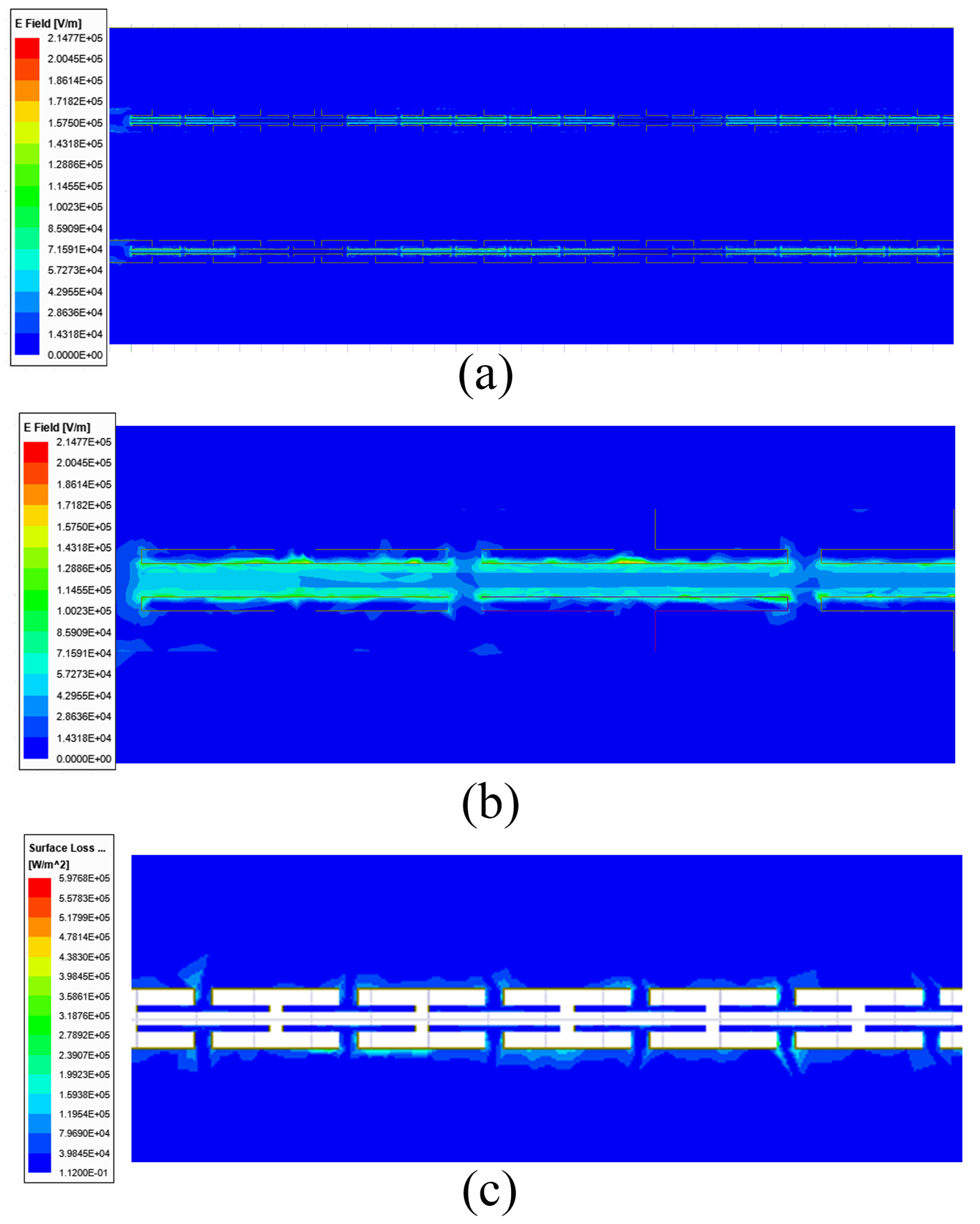
The distribution of MW in the simulation is shown in
Figure 3a, as we expect, the MW mainly distributes between the T electrodes, and by changing the initial phase at the ports, we can directly observe the microwave signal propagating along the electrode. Thus, it can be proven that this electrode model is a model that conforms to the actual working state of the electrode. The electromagnetic loss map of the electrode is shown in
Figure 3b, and it can be seen that the main loss of the microwave signal occurs in the part between the two T electrodes when propagating along the electrode. These losses will be converted into heat, thus causing the temperature of the modulator to increase.
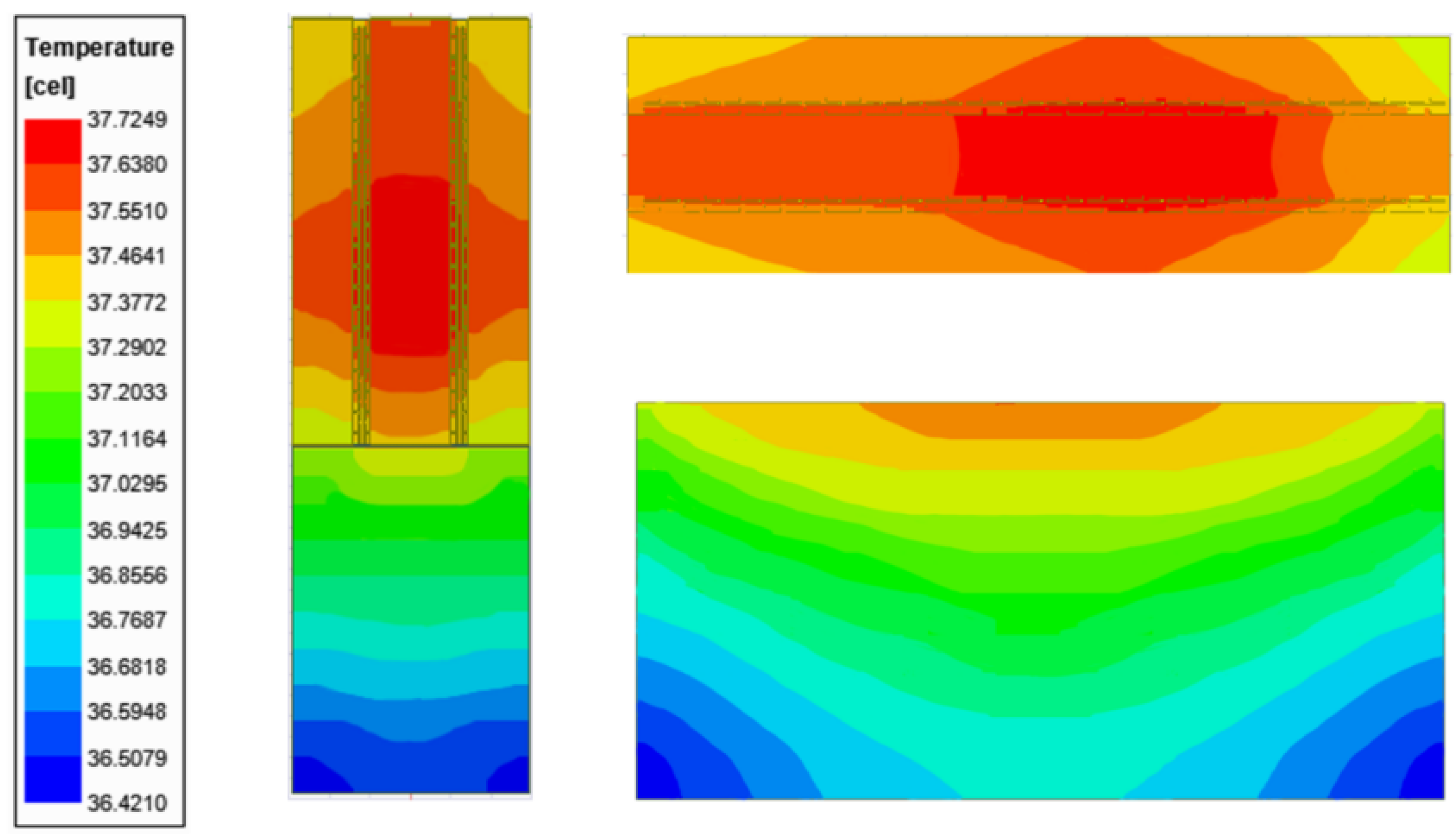
The temperature variation caused by the electromagnetic heat of the modulator electrode is shown in
Figure 4. We can see that compared to the set room temperature of 20
C, the maximum temperature increase caused by the electromagnetic heat is 17.72
C, and the minimum temperature increase is 16.42
C. As electromagnetic loss occurs near the T electrodes, the electromagnetic loss in the central part of the electrode is relatively high and the heat dissipation condition is poor. Therefore, the temperature in the center of the electrode is relatively high.
The temperature variation over time of the device’s highest and lowest temperatures is shown in
Figure 5a. We can see that after approximately 50 ms, the temperature of the device reaches a steady-state. Additionally,
Figure 5b shows the variations in the highest and lowest temperatures of the LN modulator with respect to the microwave signal frequency. With an increase in the microwave signal frequency, the temperature gradually increases, and the temperature difference between the highest and lowest temperatures also gradually increases.The results fully demonstrate that with the increase in microwave signal, the microwave heating cannot be ignored. Not only does the temperature rise affect the performance of the modulator and other components, but the uneven temperature distribution also introduces temperature interference. Therefore, in higher frequency and highly sensitive thin film LN modulators in the future, temperature control is necessary.
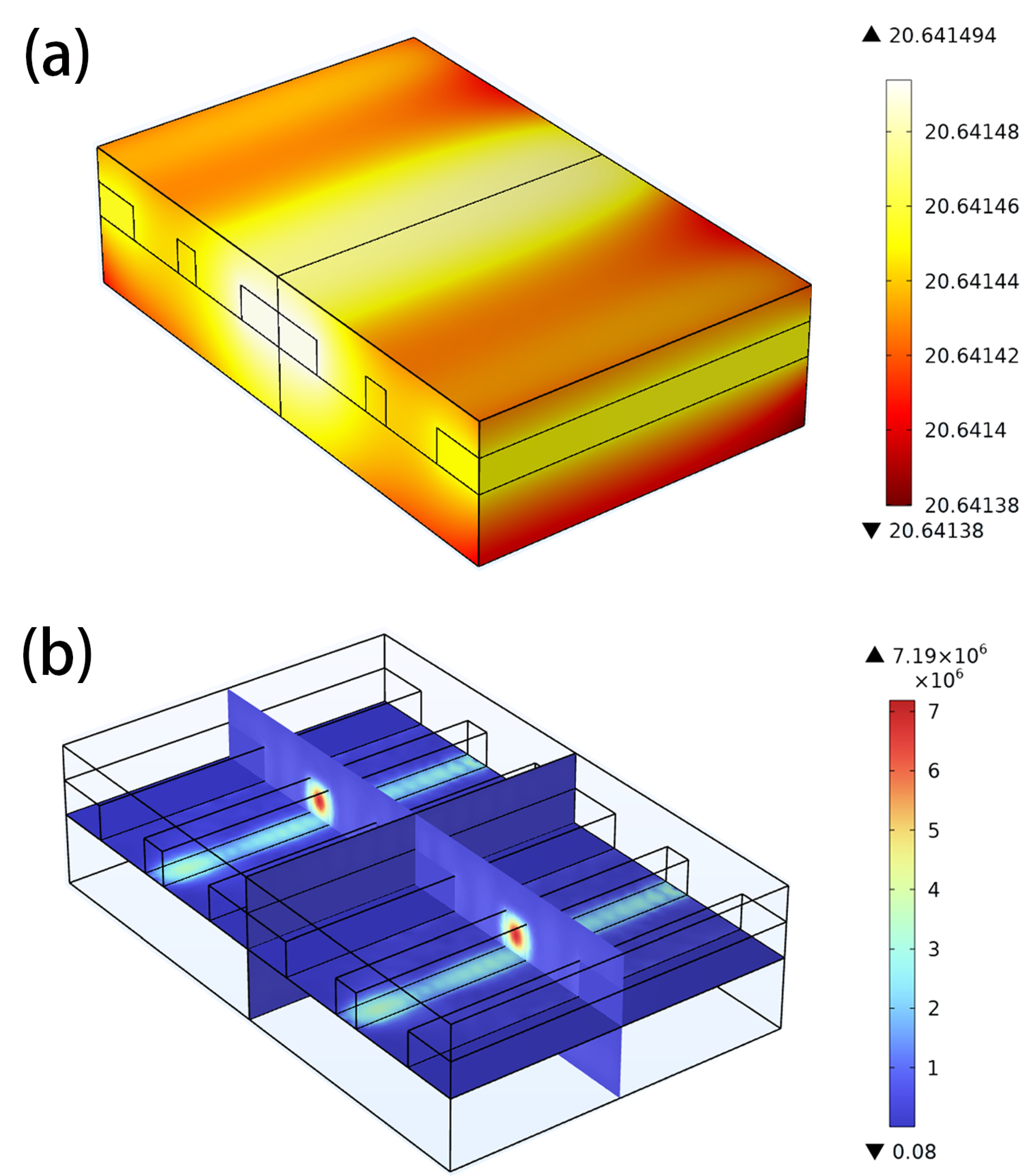
For thermal effects generated by light, because of the small length scale of the light wavelength, we cut out a 0.05 mm section from the entire modulator for simulation. In this part, we use the COMSOL Multiphysics simulation software to calculate the thermal generation of optical signal. The mesh is automatically divided using the “small” option as the default setting. During the convergence process, the maximum allowable error for the electric field is set to 0.001 V/m, and the maximum allowable error for temperature is set to 0.00001
C. The thermodynamic simulation conditions were set unchanged, with an optical signal power of 0.001 W injected into the two LN waveguides. The results are shown in
Figure 6. From the results, we can see that compared to the standard room temperature of 20
C, the maximum temperature increase caused by the optical field is 0.6415
C, and the minimum temperature increase is 0.6413
C. The heating occurred mainly on the metal electrode, indicating that the primary cause of heating was electromagnetic loss due to the light field leakage onto the surface of the metal electrode. The main heating mechanism is the same as that of the MW, but the magnitude is much smaller than that of the MW. Therefore, there is no need to consider the heat generated by the optical field, we will ignore the thermal effects generated by light in the subsequent research.
4. The Influence of the Thermal Field on the MW and the Light
As previously stated, the thermal field alters the electrical conductivity of the metal electrodes leading to an effect on the microwave electrical signal. To study the influence of electromagnetic–thermal coupling on the MW signal, we can compare the variations of the electrode’s S-parameters. S-parameters (scattering parameters) are a set of frequency-domain network parameters widely used in radio-frequency engineering and microwave engineering for characterizing the behavior of linear electrical networks, such as amplifiers, filters, and antennas. They describe the relationship between incident and reflected waves traveling in a linear electrical network based on the input/output ports of the network. S21 and S11 are two commonly used S-parameters. S21 parameter describes the transmission of a network, which is the ratio of the amplitude of the output signal to the amplitude of the input signal when the input signal is applied to Port 1 and the output signal is measured at Port 2. S11 parameter, on the other hand, describes the reflection of a network, which is the ratio of the amplitude of the reflected wave to the amplitude of the incident wave when the incident wave is applied to Port 1 and the reflected wave is measured at Port 1. In summary, S21 parameter characterizes the transfer of a signal from one port of a device to another port, while S11 parameter characterizes the reflection of a signal at a single port.
Figure 7a illustrates the variation in S21 under ideal 20
C temperature conditions and while considering the effect of electromagnetic–thermal coupling versus frequency. We observe that the temperature increase due to electromagnetic–thermal coupling reduces the S21 parameter of the electrodes, thereby decreasing the transmission rate of the MW signal. Furthermore, as the frequency of the MW signal increases, the decrease in S21 becomes more apparent, resulting in signal integrity issues and limiting the modulation rate.
In contrast, for the S11 parameter, we observe no effect on the electrodes’ reflection coefficient caused by electromagnetic-thermal coupling. This implies that the temperature increase is insufficient to alter the reflection coefficient of the electrodes.The temperature rise caused by the heat generated by microwave signals will not cause additional microwave reflections.
On the other hand, the phase stability of a modulator in real-world applications is significantly affected by temperature, leading to a phase shift during modulation that can alter the steady voltage point and increase the instability of the active device. Thus, it is necessary to investigate the temperature effect on phase and temperature field distribution within the modulator for optimized device design. The refractive index changes with temperature, thus introducing a phase shift for the propagating light. The effective refractive index of the waveguide can be easily obtained through simulation software (HFSS, Comsol), so we use the effective refractive index of the waveguide at room temperature of 20
C as a reference. The optical path variation in the light signal is obtained by multiplying the effective refractive index difference by the length of the modulator waveguide. Finally, the thermal phase shift caused by the temperature field is obtained by multiplying the optical path variation by the wave attenuation of the light signal. The variation over time of the phase shift on the left and right arms of the modulator is depicted in
Figure 8, revealing a similar trend with temperature as in
Figure 5a. Within a certain range, the relationship between temperature and phase shift is approximately proportional. However, due to non-uniform temperature distribution, there exists a difference in phase shift between the left and right arms, which may interfere with the modulation of the optical signal in practice. These thermal noises will limit the modulation accuracy of the modulator and hinder the further improvement of the modulation speed of the modulator.
5. Optimization of Modulator Design
As mentioned earlier, at high frequencies, temperature not only affects the S21 parameter of the electrode, reducing the quality of MW signal, but also causes phase shift, which interferes with the phase modulation of the optical signal, so some measures need to be taken to reduce any negative effects. Currently, the diamond heat dissipation structure is one of the most effective methods.
The diamond heat dissipation structure is achieved by embedding diamond heat dissipation sheets on the surface of the chip or package [
15,
16]. Currently, many methods have been proposed for bonding diamond heat sink layers onto metals. The most common and mature method is to grow polycrystalline diamond layers on metals using CVD [
17]. Therefore, this paper also chooses polycrystalline diamond as the heat sink layer. This structure can effectively increase the heat dissipation capacity of the chip, thereby reducing the overall temperature and minimizing the parameter drift caused by temperature changes. Moreover, it can make the temperature distribution more uniform, reducing the phase difference between the two arms caused by uneven temperature distribution. At the same time, the diamond heat dissipation structure can also improve the reliability and longevity of the device because it can effectively remove heat and reduce damage to the device caused by heat. In the past, diamond heat dissipation structures have been applied more to devices such as lasers [
18]; however, we attempted to apply it to modulators.
We have incorporated a 10
m thick diamond heat dissipation layer onto the previously modeled modulator and maintained other simulation conditions constant. The temperature distribution before and after the addition of the diamond heat dissipation layer is shown in
Figure 9 (the diamond layer is hidden for ease of visualization). Compared with the room temperature of 20
C, the maximum temperature of the modulator increased by 17.72
C before optimization and by 12.61
C after optimization. The temperature rise decreased by 28.84%, and the metal surface temperature distribution is more uniform after the inclusion of the diamond heat dissipation layer. The phase shift results after the inclusion of the diamond layer are presented in
Figure 10b. Compared to
Figure 10a, the thermal phase shift of the two-arm optical signal is similar to the temperature variation. The average thermal phase shift of the two arms decreased from 0.086
to 0.060
, a decrease of 30.2%.
At the same time, the thermal phase shift difference between the two arms significantly decreased, indicating a significant reduction in the modulator thermal noise. Therefore, the diamond heat dissipation layer has effectively reduced the interference from the temperature rise on the optical signal phase modulation.
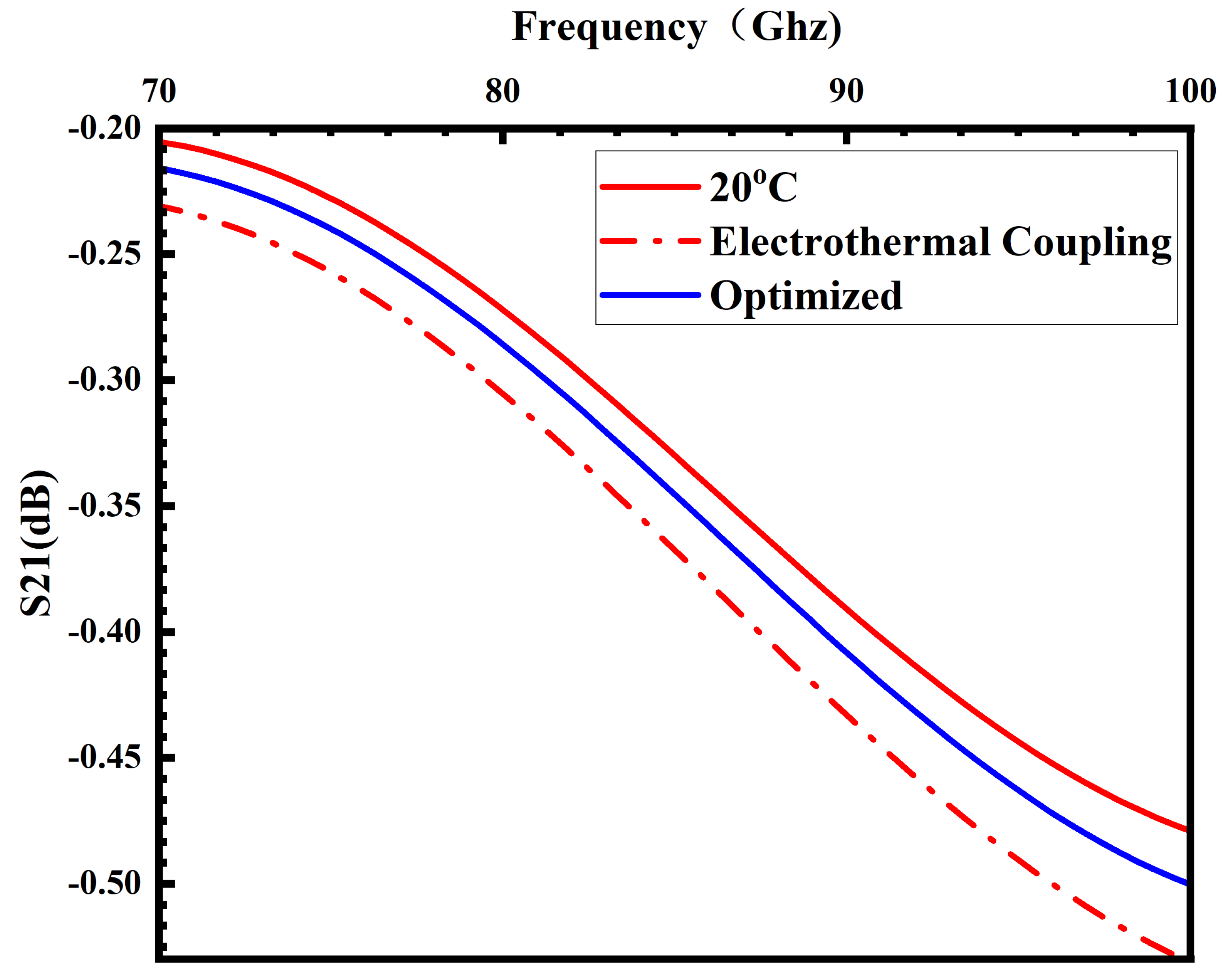
Figure 11 shows the S21 parameter after incorporating the heat dissipation layer. Taking 100 GHz as an example, compared to the ideal constant temperature of 20
C, the S21 decreased by 0.07 dB before optimization and decreased by 0.02 dB after optimization. The effect of S21 caused by temperature was optimized by 71.4%.The results indicate that the S21 parameter has been significantly improved compared to the LN modulator without the heat dissipation layer.
In addition, this paper only explores the thermal characteristics improvement of thin-film LN modulators with a diamond heat dissipation layer as an example. In fact, any material with high thermal conductivity can be used as a heat dissipation layer to improve the thermal characteristics of the modulator. The actual performance of different materials still needs to be verified through experiments. Furthermore, this study only investigates the effect of the heat dissipation layer on the optical and microwave signals of a single modulator. In fact, this improvement can also bring many benefits to photonics integrated systems, including reducing the thermal crosstalk between modulator arrays and improving the reliability of the system.
6. Conclusions
In this study, we developed a simulation model of a modulator equipped with slow-wave electrodes using geometric parameters obtained from Ref. [
12]. The heat generation of MW and light signals were analyzed, and we found that the heat generated by light signals was negligible compared to that generated by MW signals. The temperature of the modulator significantly increased with an increasing MW signal frequency. Furthermore, the impact of heat generation on MW and light signals was investigated. We found that elevated temperature not only reduced the S21 parameter of the electrode and the quality of the MW signal, but also caused a phase shift that interfered with the phase modulation of the light signal. Finally, a diamond heat dissipation layer was added to effectively improve the modulator’s thermal condition, enhance the S21 parameter, and reduce the interference of temperature on the phase modulation of the light signal. In this study, our focus was solely on the electro-optic effect of LN and its simulation solely based on electric field variations. However, it is worth noting that our investigation did not encompass the impact of other factors such as photorefraction in LN [
19] on the multi-physical coupling response. To address this, we intend to conduct more comprehensive research in the future by reconfiguring our model and performing more refined analyses. Furthermore, we hope to explore the influence of additional techniques, such as the application of surface metallization on LN [
20], in order to achieve more precise and comprehensive research outcomes.
Author Contributions
Conceptualization, J.S., G.Y., D.G. and X.W.; methodology, J.S. and G.Y.; software, J.S. and G.Y.; validation, J.S., G.Y., D.G. and X.W.; formal analysis, J.S., G.Y., D.G. and X.W.; investigation, J.S. and G.Y.; resources, M.L., N.Z. and X.W.; data curation, J.S. and G.Y.; writing—original draft preparation, J.S.; writing—review and editing, J.S. and G.Y.; visualization, J.S.; supervision, X.W.; project administration, X.W.; funding acquisition, X.W. All authors have read and agreed to the published version of the manuscript.
Funding
This work was supported by The Chinese National Key Basic Research Special Fund (2018YFE0201200) and The Strategic Priority Research Program of Chinese Academy of Sciences, Grant No.XDB43000000.
Institutional Review Board Statement
Not applicable.
Informed Consent Statement
Not applicable.
Data Availability Statement
Not applicable.
Conflicts of Interest
The authors declare no conflict of interest.
References
- Rahim, A.; Hermans, A.; Wohlfeil, B.; Petousi, D.; Kuyken, B.; Thourhout, D.V.; Baets, R. Taking silicon photonics modulators to a higher performance level: State-of-the-art and a review of new technologies. Adv. Photonics 2021, 3, 23. [Google Scholar] [CrossRef]
- Wooten, E.; YiYan, A.; Murphy, E.; Lafaw, D.; Maack, P.H.D.; Attanasio, D.; Fritz, D.; McBrien, G.; Bossi, D.; Kissa, K. A review of lithium niobate modulators for fiber-optic communications systems. IEEE J. Sel. Top. Quantum Electron. A Publ. IEEE Lasers Electro-Opt. Soc. 2000, 6, 69–82. [Google Scholar] [CrossRef]
- Lin, J.; Bo, F.; Cheng, Y.; Xu, J. Advances in on-chip photonic devices based on lithium niobate on insulator. Photonics Res. 2020, 8, 1910. [Google Scholar] [CrossRef]
- Wang, C.; Zhang, M.; Chen, X.; Bertrand, M.; Shams-Ansari, A.; Chandrasekhar, S.; Winzer, P.; Loncar, M. Integrated lithium niobate electro-optic modulators operating at CMOS-compatible voltages. Nature 2018, 562, 101–104. [Google Scholar] [CrossRef] [PubMed]
- Janner, D.; Tulli, D.; Garcia-Granda, M.; Belmonte, M.; Pruneri, V. Micro-structured integrated electro-optic LiNbO3 modulators. Laser Photonics Rev. 2009, 3, 301–313. [Google Scholar] [CrossRef]
- Sun, S.; He, M.; Xu, M.; Zhang, X.; Ruan, Z.; Zhou, L.; Liu, L.; Liu, L.; Yu, S.; Cai, X. High-Speed Modulator With Integrated Termination Resistor Based on Hybrid Silicon and Lithium Niobate Platform. J. Light. Technol. A Jt. IEEE/OSA Publ. 2021, 39, 1108–1115. [Google Scholar] [CrossRef]
- Yang, F.; Fang, X.; Chen, X.; Zhu, L.; Zhang, F.; Chen, Z.; Li, Y. Monolithic thin film lithium niobate electro-optic modulator with over 110 GHz bandwidth. Chin. Opt. Lett. 2022, 20, 148–152. [Google Scholar] [CrossRef]
- Arizmendi, L. Photonic applications of lithium niobate crystals. Phys. Status Solidi A Appl. Res. 2004, 201, 253–283. [Google Scholar] [CrossRef]
- Morse, J.; Mccammon, K.; Mcconaghy, C.; Masquelier, D.; Garrett, H. Characterization of lithium niobate electro-optic modulators at cryogenic temperatures. Proc. SPIE-Soc. Opt. Eng. 1994, 2150, 283–291. [Google Scholar]
- Cheng, W.; Zhang, M.; Stern, B.; Lipson, M.; Loncar, M. Nanophotonic Lithium Niobate Electro-optic Modulators. Opt. Express 2017, 26, 1545–1555. [Google Scholar]
- Hou, C.; Ma, T.; Gao, J.; Liu, H.; Wang, F. Mid-infrared electro-optic modulator based on a graphene-embedded plasmonic rib waveguide with ultrahigh electro-optic wavelength tuning. Appl. Opt. 2021, 60, 2795–2802. [Google Scholar] [CrossRef] [PubMed]
- Kharel, P.; Reimer, C.; Luke, K.; He, L.; Zhang, M. Breaking voltage-bandwidth limits in integrated lithium niobate modulators using micro-structured electrodes. Optica 2021, 8, 357–363. [Google Scholar] [CrossRef]
- Ma, W.; Wang, H.; Cao, B. Experimental Study on Electrical and Thermal Conductivity Properties of Gold Nanofilm. J. Eng. Thermophys. 2009, 30, 1907–1909. [Google Scholar]
- Shao, G.; Wu, Z.; Chen, J.; Xu, F.; Lu, Y. Nonlinear frequency conversion of fields with orbital angular momentum using quasi-phase-matching. Phys. Rev. A 2013, 88, 063827-1–063827-7. [Google Scholar] [CrossRef]
- Chen, P.H.; Lin, C.L.; Liu, Y.K.; Chung, T.Y.; Liu, C.Y. Diamond Heat Spreader Layer for High-Power Thin-GaN Light-Emitting Diodes. IEEE Photonics Technol. Lett. 2008, 20, 845–847. [Google Scholar] [CrossRef]
- Xie, R.; Li, Z.; Guo, S.; Wang, Z.; Xue, H. High bandwidth GaN-based blue LEDs using Ag-grating and diamond heat sink. Photonics Nanostructure-Appl. 2020, 42, 100856. [Google Scholar] [CrossRef]
- Liu, X.; Luo, H.; Su, Y.; Yu, Z. Preparation of diamond/Cu microchannel heat sink by chemical vapor deposition. J. Cent. South Univ. 2015, 22, 835–841. [Google Scholar] [CrossRef]
- Yang, Q.; Zhao, J.; Huang, Y.; Zhu, X.; Fu, W.; Li, C.; Miao, J. A diamond made microchannel heat sink for high-density heat flux dissipation. Appl. Therm. Eng. 2019, 158, 113804. [Google Scholar] [CrossRef]
- Kong, Y.; Bo, F.; Wang, W.; Zheng, D.; Liu, H.; Zhang, G.; Rupp, R.; Xu, J. Recent progress in lithium niobate: Optical damage, defect simulation, and on-chip devices. Adv. Mater. 2020, 32, 1806452. [Google Scholar] [CrossRef] [PubMed]
- Wang, C.; Su, H.; Zhang, J.; Zhao, H. Surface metallization from ab initio theory and subwavelength coupling via surface plasmon polaritons in Cu-doped lithium niobate/tantalate owing to charge accumulation. Appl. Surf. Sci. 2021, 551, 149294. [Google Scholar] [CrossRef]
Figure 1.
Low-voltage high-bandwidth traveling-wave integrated LN modulator with segmented electrodes. (a) Artistic top view of the modulator design (not to scale) where RF signal co-propagates with the optical signal. (b) Artistic vertical view of the modulator design (not to scale). (c) Cross sectional view of the phase shifter. Design parameters (g, m, s, t, r, c, ws, wb, wt, h1, h2, h3) = (5, 6, 2, 6, 45, 5, 100, 2, 2.5, 0.8, 0.3, 0.35) µm.
Figure 2.
Multi-physics relationships inside the modulator.
Figure 2.
Multi-physics relationships inside the modulator.
Figure 3.
(a) Overall MW distribution diagram of the modulator. (b) Local MW distribution diagram of the modulator. (c) MW Loss distribution of the modulator.
Figure 3.
(a) Overall MW distribution diagram of the modulator. (b) Local MW distribution diagram of the modulator. (c) MW Loss distribution of the modulator.
Figure 4.
Temperature distribution of the modulator.
Figure 4.
Temperature distribution of the modulator.
Figure 5.
(a)The variation in temperature with time. (b) The variation in temperature with frequency.
Figure 5.
(a)The variation in temperature with time. (b) The variation in temperature with frequency.
Figure 6.
(a) Temperature distribution of the modulator. (b) Light distribution of the modulator.
Figure 6.
(a) Temperature distribution of the modulator. (b) Light distribution of the modulator.
Figure 7.
(a) S21 with 20 C and electro-thermal coupling. (b) S11 with 20 C and electro-thermal coupling.
Figure 7.
(a) S21 with 20 C and electro-thermal coupling. (b) S11 with 20 C and electro-thermal coupling.
Figure 8.
The variation in phase shift with time.
Figure 8.
The variation in phase shift with time.
Figure 9.
Temperature distribution: (a) before optimization and (b) after optimization.
Figure 9.
Temperature distribution: (a) before optimization and (b) after optimization.
Figure 10.
The variation in phase shift with time: (a) before optimization and (b) after optimization.
Figure 10.
The variation in phase shift with time: (a) before optimization and (b) after optimization.
Figure 11.
S21 before and after optimization.
Figure 11.
S21 before and after optimization.
| Disclaimer/Publisher’s Note: The statements, opinions and data contained in all publications are solely those of the individual author(s) and contributor(s) and not of MDPI and/or the editor(s). MDPI and/or the editor(s) disclaim responsibility for any injury to people or property resulting from any ideas, methods, instructions or products referred to in the content. |
© 2023 by the authors. Licensee MDPI, Basel, Switzerland. This article is an open access article distributed under the terms and conditions of the Creative Commons Attribution (CC BY) license (https://creativecommons.org/licenses/by/4.0/).
