Abstract
A photonic integrated interference imaging system (PIIIS) is a computational imager based on Michelson interference and photonic integrated circuits (PICs). In this paper, a PIIIS based on a compact sampling lenslet array that can sample the zero spatial frequency through a single lenslet, densely sample the frequency in the azimuth direction through the configuration of a hierarchical multistage lenslet array, and continuously sample the frequency in the radial direction through a Langford sequence is proposed. We introduce the design process of the compact sampling lenslet array in detail and simulate the imaging of the system. The simulation results demonstrate that the lenslet array can effectively improve the imaging quality of a PIIIS. In addition, we design a silicon PIC and a silicon nitride transition PIC that match the compact sampling lenslet array and simulate the imaging of the system under the influence of the on-chip optical loss of PICs (the average interference baseline loss is 15.4 dB at 1550 nm). The results show that on-chip optical loss mainly affects the brightness and contrast of the reconstructed image but has little effect on the structure.
1. Introduction
Due to diffraction, the aperture of a traditional optical remote sensing imaging system limits the angular resolution of the system, which cannot be indefinitely increased due to the limitations of material, technology, weight, and payload volume [1]. The Segmented Planar Imaging Detector for Electro-optical Reconnaissance (SPIDER) is a novel imager based on Michelson interference and photonic integrated circuits (PICs), proposed by Lockheed Martin [2,3,4]. A lenslet array instead of a small aperture telescope array is used to simultaneously form multiple interference baselines in multiple directions, and a PIC is used to miniaturize the beam combination hardware [5]. Compared with a conventional telescope and a long baseline interferometric array with the same angular resolution, a photonic integrated interference imaging system (PIIIS) such as SPIDER can reduce the size, weight, power, and manufacturing cycle of the system and simultaneously sample all spatial frequencies with fast and high-resolution imaging [5,6]. Therefore, a PIIIS is very suitable for space-based remote sensing imaging systems.
Much research has been completed on SPIDER. S. T. Thurman et al. studied the system structure and performed a conceptual verification experiment [2,7]. S. J. B. Yoo et al. designed, fabricated, and demonstrated a silicon PIC and a silicon nitride PIC and carried out imaging experiments with the silicon nitride PIC, proving the feasibility of this technology [4,5,6]. Moreover, many researchers have completed further research on this technology in recent years, and the results show that increasing the coverage of the spatial frequency is the key factor in improving the imaging quality of a PIIIS [8,9,10].
Generally, the structure of the image is determined via the medium and low frequencies, the details are determined via the high frequency, and the average brightness distribution is determined via the zero frequency. In order to further improve the imaging quality of a PIIIS, Weiping Gao et al. proposed a hierarchical multistage sampling lenslet array, which can increase the coverage of the medium and low frequencies [11]. However, the lenslet array can neither continuously sample the high frequency nor sample the zero frequency. Huiling Hu et al. proposed a dense azimuth lenslet array and realized the continuous sampling of all integer multiples’ fundamental frequencies, including the zero frequency, by using the discrete spectral matrix reconstruction method [12]. However, since the difference between the adjacent baseline lengths of this system is four times the lenslet diameter, the lenslet array cannot really achieve the continuous sampling of a frequency. Kang Cao et al. proposed a pseudo two-layer parity configuration, which can realize the continuous coverage of the baseline length from 1 to [13]. However, since the beam behind each lenslet is divided into two parts, this configuration would increase the PIC complexity and reduce the signal-to-noise ratio of the system due to the decrease in optical power.
In order to enable a PIIIS to sample the zero frequency and to increase the coverage of the spatial frequency in the azimuth and the radial direction, a compact sampling lenslet array is proposed. The lenslet array adopts the basic structure of a hierarchical multistage lenslet array, determines the lenslet pairing method using a Langford sequence, and configures a single lenslet on each long interference arm. In this paper, the design process of the compact sampling lenslet array is introduced in detail, and the imaging of a PIIIS based on the lenslet array is simulated. Meanwhile, through the optimization of key photonic components, we design a silicon PIC and a silicon nitride transition PIC that match the lenslet array and simulate the imaging of the system under the influence of on-chip optical loss and random phase noise.
2. Imaging Principles
2.1. Propagation of Light Field from Source to Lenslet Array
A PIIIS is suitable for imaging remote targets. The light emitted by distant objects can spread to the lenslet array through Fraunhofer diffraction. As shown in Figure 1, if the complex amplitude of the light field on the object plane is , then the complex amplitude of the light field on the incident plane of the lenslet array, , is as follows:
where is the wavelength of the incident light, is the distance between the object plane and the lenslet array plane, is the wave number, and is the spatial frequency coordinate on the incident plane of the lenslet array.
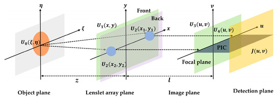
Figure 1.
Schematic diagram of propagation process of light from object plane to detection plane.
The lenslet array would modulate the phase and size of the incident wavefront, and the complex amplitude transmittance of any lenslet is as follows:
where is the lenslet diameter, is the focal length of the lenslet, is the center coordinate of the jth lenslet in the lenslet array, and is the total number of lenslet in the system. After passing through the lenslet, the complex amplitude of the light field is as follows:
Finally, the light field is focused on the focal plane of the lenslet array through Fresnel diffraction, where the complex amplitude of the light field is as follows:
where is the image distance, which can be expressed by the object distance and the focal length according to Gaussian formula , and is the spatial frequency coordinate on the focal plane of the lenslet array.
2.2. Detection of Mutual Coherent Intensity
The light field on the focal plane of the lenslet array is coupled into the input waveguide on the PIC. For a single waveguide, the coupling efficiency between the light field on the focal plane and the input waveguide is defined as follows [14]:
where is the electric field on the focal plane, is the fundamental mode electric field of the waveguide, and denotes complex conjugation.
Therefore, the distribution of the light field at the input waveguide on the PIC is as follows:
Meanwhile, with the increase in field-of-view (), the coupling efficiency between spatial light and waveguide decreases rapidly. When the reaches , the coupling efficiency is about one-tenth of that at the central optical axis [15], which means that the of a single waveguide should be limited to . However, the of the system can be increased by the waveguide array behind the lenslet array. When the waveguide array is , the is as follows:
As shown in Figure 2, when the light field is coupled into the PIC, the phase shifter modulates its phase, and the AWG divides the incident broad-spectrum light into multiple narrow-spectrum lights. Then, two narrow-spectrum lights with the same central wavelength from the same pair of lenslets are coupled into a optical hybrid, and four interference signals are generated after splitting, phase shifting, and combining. The optical powers of the four output ports of the optical hybrid are as follows [16]:
where, and are the optical powers of the two input lights, respectively, and and are the initial phases of the two input lights, respectively.
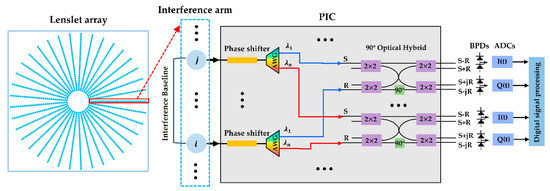
Figure 2.
Working principle of PIIIS.
The output of the four interference signals are then received by two balanced photodetectors. After photoelectric conversion and differential amplification, the in-phase current and the quadrature current are obtained as follows:
where is the responsivity of the balanced photodetector.
Therefore, the interference fringe information of two narrow spectrum lights with the same central wavelength passing through the same pair of lenslets can be obtained, that is, the phase and amplitude of the mutual coherence intensity of two coherent lights are as follows:
2.3. Image Reconstruction
Since the whole transmission process of light fields on PIC can only produce a phase delay and cannot change the distribution of light fields, the coordinate system of light fields on PIC remains unchanged [17]. According to the distribution of light fields at the input waveguide on PIC, the mutual coherent intensity between two interfering narrow-spectrum lights on the detection plane is as follows:
where is the central wavelength of the narrow-spectrum light; and are the center coordinates of the two lenslets, respectively; ; and .
Equation (13) is the Van Cittert–Zernike Theorem, which shows that on the detection plane of the imaging system, the mutual coherent intensity of the two coherent lights from a pair of lenslets is proportional to the Fourier transform of the light intensity of the observed object. Meanwhile, the spatial frequency corresponding to the interference baseline () formed by the pair of lenslets is as follows:
Therefore, according to the Van Cittert–Zernike Theorem, the system can reconstruct the image of the observed target by sampling the mutual coherent intensity information with enough spatial frequencies and performing an inverse Fourier transform on the Equation (13). Obviously, the imaging quality of the system directly depends on the coverage of spatial frequency. According to Equation (14), the spatial frequency is determined by the relative position of a pair of lenslets, wavelength , and object distance . Due to the limited ability of the spectrum division and wavelength range of AWG, the configuration of the sampling lenslet array directly determines the imaging quality of the system.
3. Compact Sampling Lenslet Array
Compared with the traditional wheel-type sampling lenslet array, the hierarchical multistage sampling lenslet array can increase the coverage of medium and low spatial frequencies [11], while the Langford sequence can be used to determine the matching method of lenslets to realize the continuous coverage of spatial frequencies in the radial direction [18]. In order to increase the spatial frequency coverage of a PIIIS in both the azimuth and radial directions, the hierarchical multistage sampling lenslet array and the Langford sequence should be combined in the design of the sampling lenslet array.
3.1. Design Process of Compact Sampling Lenslet Array
The traditional wheel-type sampling lenslet array, which uses 37 equal-length interference arms and determines the baseline length via the first-to-tail pairing method and with lenslets closely adjacent in the radial direction, is shown in Figure 3a. As shown in Figure 3b, the hierarchical multistage sampling lenslet array adopts three lengths of interference arms. It takes the interference arm of the wheel-type sampling lenslet array as the long interference arm and adds the medium interference arm on both sides of the long arm and the short interference arm on both sides of the medium interference arm.
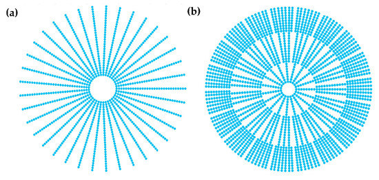
Figure 3.
(a) The traditional wheel-type sampling lenslet array. (b) The hierarchical multistage sampling lenslet array.
3.1.1. Basic Structure of Compact Sampling Lenslet Array
In order to sample zero frequency, we have added a single lenslet that is not paired with other lenslets on each long interference arm based on the structure of the hierarchical multi-stage sampling lenslet array. As shown in Figure 4, assuming that the lenslet diameter is , the number of long interference arms, medium interference arms, and short interference arms is , , and , respectively. Meanwhile, we define the innermost lenslet on each interference arm as the first lenslet. When there is no gap between the first lenslets of adjacent long interference arms, the angle formed by the adjacent long interference arms and the radius of the circle formed by the first lenslets of all long interference arms are as follows:
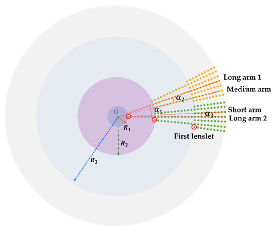
Figure 4.
Schematic diagram of the arrangement of three kinds of interference arms of compact sampling lenslet array.
To approximate the tangent value with the radian value within an acceptable error range, we require ; thus, . For effectively improving the imaging quality without increasing the cost, we take and, then, and .
When there is no gap between the first lenslets on the medium interference arm and the short interference arm or their adjacent interference arms, the angle formed by the medium interference arm and its adjacent interference arm is , and the angle formed by the short interference arm and its adjacent interference arm is . Thus, the radii of the three circles formed by all the first lenslets on three lengths of interference arms are as follows:
Therefore, to make the first lenslet of each interference arm closely contact with the adjacent interference arm, the radial distance between the medium interference arm and the long interference arm should satisfy Equation (20), while the radial distance between the short interference arm and the long interference arm should satisfy Equation (21).
In other words, if the number of lenslets forming the long interference arm, the medium interference arm, and the short interference arm are , , and , respectively ( is odd, and and are even), then the position of the first lenslet of the medium interference arm should be at least equivalent to the 14th lenslet of the long interference arm, while the position of the first lenslet of the short interference arm should be at least equivalent to the 38th lenslet of the long interference arm. As a result, the relationships between the number of lenslets on the three kinds of interference arms can be expressed by Equations (22) and (23).
3.1.2. The Number and Paring Method of Lenslets
According to the conclusions in Ref. [18], for any interference arm, if the shortest baseline length is () and the total number of paired lenslets is , then the condition for realizing baseline length distribution of is as follows:
where
In order to ensure dense coverage of low frequencies and continuous coverage of medium and high frequencies, we set the short interference arm to mainly sample low frequencies. In addition, the overlap of frequency coverage of interference arms with different lengths is required to be the least. Based on Equations (22)–(25), when the number of lenslets on the short interference arm is and its shortest baseline length is , the possible combinations of the number of lenslet in three kinds of interference arms are listed in Table 1.

Table 1.
When and , the possible combinations of the lenslet number of three kinds of interference arms.
According to Table 1, to obtain a wide range of spatial frequency coverage with fewer lenslets, we choose . Meanwhile, we take the shortest baseline length of the medium interference arm as and the shortest baseline length the long interference arm as .
If the serial number of the first lenslet on the long interference arm is set to zero, and the serial number of the first lenslet on both the medium interference arm and the short interference arm is set to one, the lenslet pairing methods and baseline lengths on the three kinds of interference arms are as follows. (1) Short interference arm: the lenslet paring method is (7,8), (1,3), (2,5), (6,10), and (4,9), and the baseline lengths are , , , and . (2) Medium interference arm: the lenslet paring method is (26,31), (8,14), (25,32), (7,15), (11,20), (23,33), (5,16), (22,34), (4,17), (13,27), (3,18), (12,28), (2,19), (6,24), (10,29), (1,21), and (9,30), and the baseline lengths are , , , , , , , , , , , , , and . (3) Long interference arm: the lenslet paring method is (17,29), (23,36), (10,24), (22,37), (9,25), (21,38), (8,26), (20,39), (7,27), (19,40), (6,28), (18,41), (11,35), (5,30), (16,42), (4,31), (15,43), (3,32), (14,44), (2,33), (13,45), (1,34), and (12,46), and the baseline lengths are , , , , , , , , , , , , , , , , and .
At this point, we have completed the design of the compact sampling lenslet array (as shown in Figure 5a), and the overall structure of a PIIIS based on compact sampling array is shown in Figure 5b.
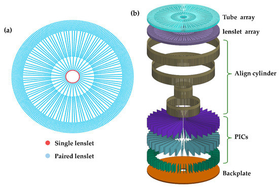
Figure 5.
(a) Structure of compact sampling lenslet array, (b) schematic diagram of the overall structure of PIIIS based on compact sampling array (layer-by-layer breakdown).
3.2. Imaging Verification of Compact Sampling Lenslet Array
In order to verify whether the compact sampling lenslet array can improve the imaging quality of a PIIIS, we use the parameters in Table 2 to simulate the spatial frequency coverage and imaging of the PIIIS with four aperture configurations, which are (1) the compact sampling lenslet array, (2) the compact sampling lenslet array without single lenslet, (3) the wheel-type sampling lenslet array using single lenslet and Langford sequence to determine the lenslet pairing method, and (4) the compact sampling lenslet array using the first-to-tail paring method. The structures of these four aperture configurations are shown in Figure 6, with the lenslet paring methods shown in Figure 7.

Table 2.
System parameters of PIIIS used for imaging simulation.

Figure 6.
Sampling lenslet array structures of four aperture configurations for imaging simulation of PIIIS. (a) Structures of aperture configurations (1) and (4), (b) structure of aperture configuration (2), and (c) structure of aperture configuration (3).

Figure 7.
Lenslet paring methods of four aperture configurations for imaging simulation of PIIIS (the numbers in the figure indicate the serial numbers of the lenslet, and they increase from the center of the circle to the outside in turn). (a) Lenslet paring methods of aperture configurations (1) and (2), (b) lenslet paring methods of aperture configuration (3), and (c) lenslet paring methods of aperture configuration (4).
In Table 2, we set the working waveband to 1500–1600 nm in consideration of the actual process level of silicon PIC [19]. According to the parameters in Table 2, the of a single waveguide is , the Nyquist sampling spacing is , and the ultimate angular resolution of the system is . We limit the of the system to pixels in the imaging simulation and use the resolution board as shown in Figure 8a as the imaging target, with Figure 8b showing its spatial spectrum distribution. Furthermore, in order to quantitatively analyze the imaging quality and to compare the similarities between the reconstructed image and the original image, peak signal-to-noise ratio (PSNR), mean square error (MSE), and structural similarity (SSIM) are used as evaluation functions.
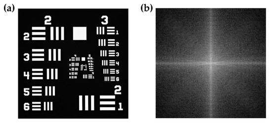
Figure 8.
(a) Light intensity distribution of the original image. (b) Spatial spectrum distribution of the original image.
The spatial frequency coverage of a PIIIS based on the above four aperture configurations is shown in Figure 9. As can be seen from Figure 9b, the existence of a single lenslet can enable the system to sample zero frequency. Based on Figure 9a,c, compared with the wheel-type sampling lenslet array, the hierarchical multistage sampling lenslet array covers the medium and low frequencies more closely in azimuth. For the third aperture configuration, the longest baseline is and the maximum sampling radius is 0.0958. A comparison between Figure 9a,d demonstrates that the spatial frequency range covered by the lenslet pairing method determined via Langford sequence is small and compact, with the longest baseline of and the maximum sampling radius of 0.1357, while the spatial frequency range covered by the first-to-tail lenslet pairing method is large and sparse, with the longest baseline of and the maximum sampling radius of 0.1796.
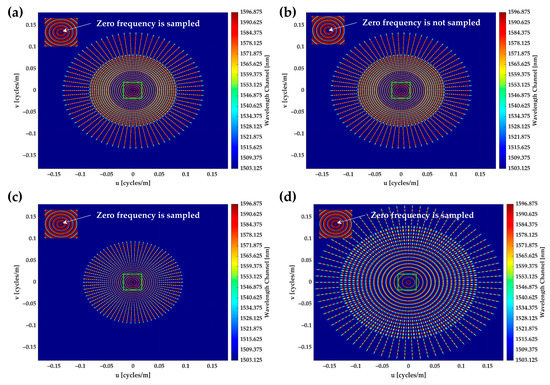
Figure 9.
(a) Spatial frequency coverage of aperture configuration (1), (b) spatial frequency coverage of aperture configuration (2), (c) spatial frequency coverage of aperture configuration (3), and (d) spatial frequency coverage of aperture configuration (4).
The imaging results of a PIIIS based on the four aperture configurations are shown in Figure 10. According to the MSE, PSNR, and SSIM of the reconstructed images, the order of the imaging quality of the four aperture configurations from high to low is (1) > (3) > (4) > (2). As can be seen from Figure 10a, the imaging quality with the compact sampling lenslet array is the best, and the brightness distribution, contrast, and structure of the reconstructed image are the closest to the original image. From Figure 10b, when a PIIIS does not sample zero frequency, the reconstructed image is only similar to the original image in structure, while the overall brightness distribution and contrast are quite different, and the imaging quality is poor. From Figure 10c, the imaging quality based on the third aperture configuration is poor, the constructed image is blurred, and the details are difficult to distinguish. Therefore, the contrast and contour of the reconstructed image are quite different from the original image. It can be seen from Figure 10d that the imaging quality of the fourth aperture configuration is also poor. However, though the contrast and contour of the reconstructed image are different from the original image, the boundaries are clear and distinguishable.
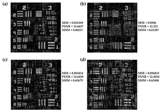
Figure 10.
(a) Simulation imaging result of PIIIS based on aperture configuration (1), (b) simulation imaging result of PIIIS based on aperture configuration (2), (c) simulation imaging result of PIIIS based on aperture configuration (3), and (d) simulation imaging result of PIIIS based on aperture configuration (4).
Because the medium and low frequencies determine the structure of an image, the high frequency determines the details, and the zero frequency determines the average brightness distribution, the imaging results in Figure 10 should be essentially determined via the spatial frequency coverage characteristics of each aperture configuration. Meanwhile, the above results prove that the imaging quality of a PIIIS can be effectively improved by using a compact sampling lenslet array.
4. Design and Layout of PIC
On the PIC required by a PIIIS, key components such as phase shifter, multi-mode interferometer (MMI), and AWG are integrated, and the beam is path-length-matched, phase-shifted, wavelength-divided, and combined on the PIC. According to the structure of the compact sampling lenslet array in the previous section, we have designed a processing PIC and a transition PIC used for coupling light beams into the processing PIC.
Considering the actual process level, we take 1550 nm as the central wavelength of PIC component design and set the detection waveband to 1500–1600 nm. In this band, due to the low the transmission loss of the silicon nitride waveguide [20,21], we choose silicon nitride as the material of the core waveguide of the transition PIC that requires long-distance transmission. Meanwhile, due to the strong constraint of silicon waveguide to light field, low loss, and the small size of a silicon-integrated device [19,22], the core waveguide of the processing PIC adopts silicon.
4.1. Design of Key Components
4.1.1. Core Waveguide
We chose a core waveguide thickness of 220 nm for silicon PIC and 400 nm for silicon nitride PIC. Under this condition, the relationships between the effective refractive index and the waveguide width of the two waveguides are shown in Figure 11. Therefore, in order to make both waveguides meet the single-mode transmission conditions, we chose the widths of silicon waveguide and silicon nitride waveguide to be 400 nm and 1000 nm, respectively. The mode profiles of transverse electric (TE) polarized light in the two waveguides are shown in Figure 12.

Figure 11.
(a) The relationship between effective refractive index of silicon waveguide and its width (waveguide thickness is 220 nm). (b) The relationship between effective refractive index of silicon nitride waveguide and its width (waveguide thickness is 400 nm).
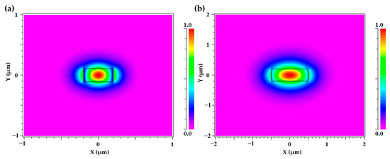
Figure 12.
(a) The mode profile of TE polarized light in a silicon waveguide, 400 nm wide and 220 nm tall. (b) The mode profile of TE polarized light in a silicon nitride waveguide, 1000 nm wide and 400 nm tall.
Meanwhile, the bending losses of the two waveguides are shown in Figure 13. We chose the minimum bending radius of silicon waveguide to be 8 (its bending loss is dB/cm), and the minimum bending radius of silicon nitride waveguide to be 40 (its bending loss is dB/cm).

Figure 13.
(a) Bending loss as a function of bending radius for a silicon waveguide, 400 nm wide and 200 nm tall. (b) Bending loss as a function of bending radius for a nitride silicon waveguide, 1000 nm wide and 400 nm tall.
The crosstalk of the two waveguides in the horizontal (width) direction is shown in Figure 14. We chose the minimum horizontal spacing of silicon waveguide to be 2 (its coupling coefficient is dB/cm) and the minimum horizontal spacing of silicon nitride waveguide to be 4 (its coupling coefficient is dB/cm).
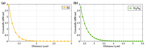
Figure 14.
(a) Relationship between horizontal crosstalk and distance between two silicon waveguides. (b) Relationship between horizontal crosstalk and distance between two nitride silicon waveguides.
4.1.2. Conversion, Crossing, and Coupling between Waveguides
- 1.
- Silicon nitride–silicon waveguide converter
As there is a conversion between silicon nitride PIC and silicon PIC, we designed a silicon nitride–silicon waveguide converter as shown in Figure 15a,b. The vertical spacing (in thickness direction) between the two waveguides is 0.25 , and the coupling length is 29 . In the process of the waveguide tapering from single mode to 0.18 , the light beam is coupled into the silicon waveguide from the silicon nitride waveguide. The mode intensity profiles of the fundamental TE mode in the converter are shown in Figure 15a and the loss is about 0.1 dB, and Figure 15c shows the transmission spectrum of the converter.
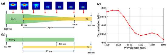
Figure 15.
Schematic of silicon nitride–silicon waveguide converter: (a) top-down view, and the mode intensity profiles of the fundamental TE mode in the interlayer coupler; (b) cross-sectional view; (c) the transmission spectrum of the silicon nitride–silicon waveguide converter.
- 2.
- Waveguide crossing
On the silicon PIC, because two input waveguides in different positions would enter the same coupler during interference, there should be inevitable crossing between waveguides. We designed a waveguide crossing based on multi-mode interference, shown in Figure 16a. The coupling length is 11.6 , the width is 1.2 , and the input and output waveguides are at single-mode width. Figure 16 shows the transmission process of the fundamental TE mode light field in the waveguide crossing, and the loss is about 0.1 dB. Figure 16c shows the transmission spectrum of the crossing waveguide.

Figure 16.
(a) Schematic of crossing waveguide, (b) the transmission process of the fundamental TE mode light field in the crossing waveguide, and (c) the transmission spectrum of the crossing waveguide.
- 3.
- Interlayer coupler
In order to integrate multiple components on a small-sized silicon PIC, we adopted a multi-layer silicon waveguide structure and designed an interlayer coupler as shown in Figure 17. Through the intermediate transition waveguide, the light field can be coupled from the top waveguide into the bottom waveguide. The vertical spacing between adjacent waveguides is 0.3 , the length of transition waveguide is 10.8 , and the vertical spacing between top waveguide and bottom waveguide is 0.82 . The transmission process of the fundamental TE mode light field in this structure is shown in Figure 17c, and the loss is about dB. Figure 17d shows the transmission spectrum of the silicon waveguide interlayer coupler.

Figure 17.
Schematic of silicon waveguide interlayer coupler: (a) top-down view, (b) cross-sectional view; (c) the transmission process of the fundamental TE mode light field in the interlayer coupler; and (d) the transmission spectrum of the interlayer coupler.
4.1.3. MMI
In order to reduce the complexity and power consumption of the silicon PIC, MMI is used as the beam combination component. We designed a MMI as shown in Figure 18a. The coupling length is 40.9 , and the width is 5.2 . The input and output waveguides are single mode widths, and all of them are located at the width of coupling width. The transmission process of the fundamental TE mode light field in MMI is shown in Figure 18b. The insertion losses of two output ports of the MMI are 3.4 dB and 3.3 dB, respectively (3 dB is the inherent loss); the splitting ratio is ; the splitting unevenness is 0.1492; and the additional loss is about 0.3 dB. Figure 18c shows the transmission spectrum of the MMI.
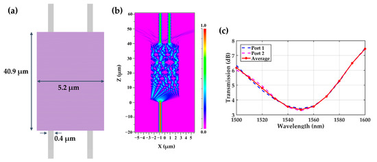
Figure 18.
(a) Schematic diagram of MMI, (b) the transmission process of the fundamental TE mode light field in MMI, and (c) the transmission spectrum of the MMI.
4.1.4. Phase Shifter
Before the light beam is coupled into MMI, it should be phase-modulated to meet the interference conditions. We designed a thermo-optic phase shifter, as shown in Figure 19a, in which TiN is used as the heating electrode. The electrode width is 1 , the thickness is 0.2 , the length is 100 , and the vertical spacing between the heating layer and the core waveguide is 1 . Figure 19b shows the phase change in core waveguide as a function of input power. When the phase change in the core waveguide reaches , the required input power is 18.7 mW; for this condition, the temperature distribution of the phase shifter is also shown in Figure 19b, and the absorption loss of the electrode layer is about dB/cm. Figure 19c shows the spectrum of absorption loss of phase shifter.

Figure 19.
(a) Schematic diagram of phase shifter; (b) the phase change in core waveguide as a function of input power, and the temperature distribution of the phase shifter when the input power is 18.7 mW; (c) spectrum of absorption loss of phase shifter.
4.1.5. AWG
In order to further reduce the size and optical loss of the silicon PIC, we designed a wavelength channel AWG, as shown in Figure 20a. The two sides of the AWG are completely symmetrical, each with an input port (outermost) and 16 output ports. The central wavelength is 1500 nm, the wavelength channel interval is 4.8 nm, the number of array waveguides is 80, and its size is .
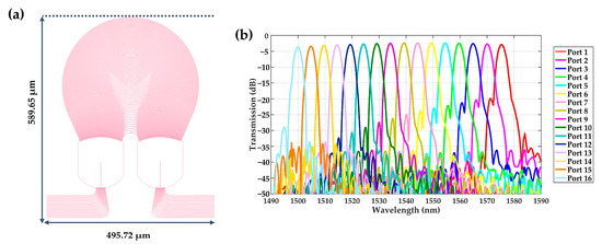
Figure 20.
(a) The layout of the 16 wavelength channel silicon AWG, (b) the simulated transmission spectrum of the 16 wavelength channel silicon AWG.
The simulated transmission spectrum of the 16 wavelength channel AWG is shown in Figure 20b. The minimum insertion loss of the central channel is 2.4 dB, the minimum insertion loss of the edge channel is 3.7 dB, the non-uniformity of the channel insertion loss is 2.1 dB, the flatness of the waveband is 0.7767, the crosstalk of adjacent channels is 18.6 dB, the crosstalk of non-adjacent channels is 37.2 dB, and the 3 dB bandwidth of central waveguide is 0.3 nm. Furthermore, the central wavelengths of 16 output channels are 1500 nm, 1504.8 nm, 1509.6 nm, 1514.4 nm, 1519.4 nm, 1524.3 nm, 1529.3 nm, 1534.2 nm, 1539.2 nm, 1544.3 nm, 1549.5 nm, 1554.5 nm, 1559.6 nm, 1564.8 nm, 1750.1 nm, and 1575.3 nm, respectively.
4.2. Layout Design
The silicon nitride transition PIC is responsible for coupling the light beams behind the lenslet array into the silicon PIC, its input waveguide spacing depends on the radial spacing between the lenslets, and its output waveguide spacing depends on the input waveguide spacing of the silicon PIC. Therefore, it is necessary to design the layout of silicon PIC first.
4.2.1. Layout Design of Silicon PIC
According to the number of lenslets and the lenslet pairing method on the long interference arm, we have designed a silicon PIC as shown in Figure 21 (the basic structure of the silicon PIC used in the medium interference arm and the short interference arm is completely consistent with it). There are 47 input waveguides and 737 output waveguides on the silicon PIC, and the size is . The input waveguide spacing is 110 , the output waveguide spacing is 4 , and the bending radius is 20 ; thus, the horizontal crosstalk and bending loss can be ignored.
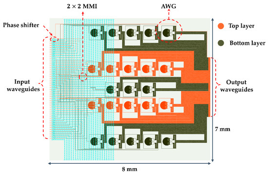
Figure 21.
Layout of multi-layer silicon PIC.
Through path-length matching, two beams of light from a pair of lenslets have the same optical path length on the silicon PIC. The average path length of interference baseline on silicon PIC is about 22.6392 mm, and the transmission loss is about 6.8 dB. Furthermore, the absorption loss of the phase shifter is dB, the average insertion loss of MMI is 3.3 dB, the average insertion loss of AWG is about 2.7 dB, and the loss of crossing waveguide is 1.1 dB (the average crossing can be 10 times). Therefore, it can be estimated that the optical loss of an average interference baseline on the silicon PIC is about 13.9 dB.
4.2.2. Layout Design of Silicon Nitride PIC
According to the input waveguide spacing of silicon PIC, we designed a silicon nitride transition PIC suitable for a long interference arm, shown in Figure 22, whose size is (the basic structure of the silicon nitride PIC used for the medium interference arm and the short interference arm is the same as that for the long interference arm, but the number of input waveguides is determined by the number of lenslets on the interference arm). The input waveguide spacing of the PIC is 3 mm, the output waveguide spacing is 110 , and the bending radius is 100 ; thus, the horizontal crosstalk and bending loss between waveguides can also be ignored.
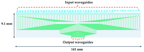
Figure 22.
Layout of silicon nitride PIC.
Through path-length matching, the path lengths of all light of beams on the silicon nitride PIC are the same. For any interference baseline, the optical path length is 29.057 mm, the transmission loss is about 1.5 dB, and the loss of the silicon nitride–silicon waveguide converter is about dB. Therefore, the optical loss of average interference baseline on the silicon nitride PIC is about 1.5 dB.
4.2.3. PIC Fabrication
The two kinds of silicon PIC designed in this work can be manufactured via the CMOS compatible process. For the first design, an 8-inch SOI wafer can be used to obtain the first layer of the strip silicon waveguide after deep ultraviolet (DUV) lithography and silicon etching. The cladding layer can be deposited via the low-pressure chemical vapor deposition (LPCVD) method, and then, the second and third silicon waveguides can be realized via the same steps. For the second design, an 8-inch SOI wafer can also be used to obtain a silicon waveguide after photolithography and etching; a layer can be deposited by LPCVD; and then, a waveguide can be formed by etching.
For the size of the waveguide designed in this paper, DUV lithography (such as 193 nm or 248 nm lithography equipment) can be used to etch the waveguide. These processes are CMOS-compatible and can be realized by silicon foundries.
4.3. Simulate the Influence of On-Chip Optical Loss and Phase Noise on Imaging
4.3.1. Influence of On-Chip Optical Loss on Imaging
When the light beam is coupled into the PIC, it causes a loss in optical power, which leads to a decrease in detection accuracy. Using the design values of the central wavelength of 16 channel AWG, considering the transmission loss of silicon waveguide and silicon nitride waveguide (take 0.5 dB/cm and 3.0 dB/cm, respectively), and the insertion loss of key components, the relationships between wavelength and average optical loss of interference baseline can be estimated, as shown in Table 3. Moreover, the optical loss of the single lenslet is about 8.2 dB.

Table 3.
Simulation values of optical loss of key components and interference baseline at design values of central wavelength of 16 channel AWG.
Using the simulated values of wavelength and average interference baseline loss in Table 2 and using the previous resolution board as the imaging target, the imaging result of a PIIIS based on the compact sampling lenslet array is shown in Figure 23. After considering the optical loss of PICs, the MSE of the reconstructed image is increased, the PSNR and SSIM are decreased, and the imaging quality of the system is significantly reduced. The brightness distribution and contrast of the reconstructed image are far from the original image, while the overall contour is still clear. In other words, the on-chip optical loss of the PIC has a great influence on the brightness and contrast of the reconstructed image (especially the contrast) but has a little influence on the structure of the image.
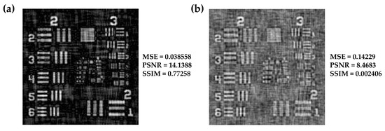
Figure 23.
Simulation imaging results of PIIIS based on compact sampling lenslet array, at design values of central wavelength of 16 channel AWG. (a) Ideal imaging result, (b) imaging result considering the on-chip optical loss of PICs.
4.3.2. Influence of Phase Noise on Imaging
Since the system error can be controlled within a certain range through stable technology and system adjustment, the form of error is similar to random distribution within a certain error range [23]. In order to analyze the influence of a phase error on the imaging quality of the system, we use the following form of random phase noise:
where represents the upper limit of the random phase noise (for example, 10%), represents a random number between 0 and , and is the phase of visibility signal.
After the random phase noise is brought into the original sampling spectrum, the change in the evaluation function of the reconstructed image is shown in Figure 24. It can be seen from Figure 24a that when the phase noise is 30%, the error variation in PSNR is about 3.99%, the error variation in SSIM is about 5.38%, and the average error variation is about 4.69% without considering the on-chip optical loss. While Figure 24b shows that when the phase noise is 30% and the on-chip optical loss is considered, the error variation of PSNR is almost zero, the error variation of SSIM is about 0.25%, and the average error variation is about 0.13%. Therefore, although the imaging quality deteriorates with the increase in phase noise, the influence of phase noise on it is relatively reduced when the on-chip optical loss reduces the imaging quality.

Figure 24.
(a) The error variations in PSNR and SSIM of the reconstructed image without considering the on-chip optical loss, (b) the error variations in PSNR and SSIM of the reconstructed image considering the on-chip optical loss.
Meanwhile, Figure 25 shows the simulated imaging results of the system when the phase noise is 30% and 60%. As can be seen from Figure 25a,c, the increase in phase error reduces the contrast and brightness and makes the outline of the image difficult to distinguish without considering the on-chip optical loss. From Figure 25b,d, it can be seen that under the influence of on-chip optical loss, the increase in phase error makes the contrast of the image decrease more obviously and the image more blurred.
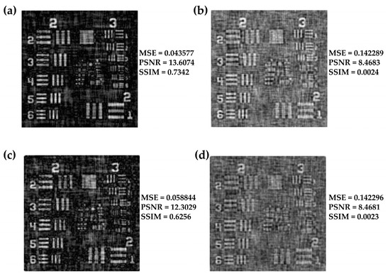
Figure 25.
(a,c) Imaging results without considering the on-chip optical loss; (b,d) imaging results considering the on-chip optical loss. (a) The phase noise is 30%. (b) The phase noise is 30%. (c) The phase noise is 60%. (d) The phase noise is 60%.
4.4. Calibration of Measurement Error of Visibility
The influence of on-chip optical loss on visibility measurement can be corrected via an online calibration method [23]. As shown in Figure 26, an optical switch is added to each input waveguide on the silicon PIC. Without considering the phase error, for any interference baseline and any wavelength channel, when both Gate 1 and Gate 2 are turned on, the two measured interference signals are as follows:

Figure 26.
Schematic diagram of visibility measurement error calibration method.
Changing the phase on one of the waveguides by , and the other two interference signals can be measured as follows:
where , , , and represent the loss coefficients of each branch; is the phase difference between the two input signals; and is the visibility. When only Gate 1 or Gate 2 is turned on, the measured signals are as follows:
Therefore, the four output interference signals that can be corrected as follows:
and, the amplitude and phase of the corrected visibility are as follows:
5. Discussion
In this study, we designed a compact sampling lenslet array used for a PIIIS and designed a silicon PIC that matches the system. Compared with the traditional wheel-type sampling lenslet array [5,6], the compact sampling lenslet array can collect the central zero frequency, make the spatial frequency coverage more continuous in the radial direction and more compact in the azimuth direction, and further increase the spatial utilization ratio of the lenslet array, thus improving the imaging quality. In the design of the PIC, we adopted a three-layer silicon waveguide structure, which is smaller in size than the three-layer silicon nitride waveguide structure adopted in Ref. [5]. In addition, we analyzed the influence of on-chip optical loss and random phase error on the imaging quality of the system and found that the existence of on-chip optical loss has little influence on the image structure, and it can be corrected via online calibration. In contrast, random phase noise affects the contrast and brightness of the image and makes the image more difficult to distinguish.
However, the influence of some practical factors on the optical power and phase, such as lenslet array alignment, coupling efficiency between the beam on the back focal plane of lenslet array and the silicon PIC, etc., has not been considered in this work. Therefore, the specific situation of the influence of the error of optical power and phase on imaging quality of a PIIIS needs further research and verification, which is also a key problem that needs to be considered before the next experimental construction.
6. Conclusions
In order to increase the spatial frequency coverage of a PIIIS, we designed a compact sampling lenslet array, which can achieve dense spatial frequency coverage in the azimuth direction and continuous sampling in the radial direction. Through numerical simulations, we have verified that the compact sampling lenslet array can effectively improve the imaging quality of a PIIIS. Meanwhile, according to the structure of the compact sampling lenslet array, we have designed a silicon PIC and a silicon nitride transition PIC that matches the lenslet array. Using the simulated values of optical loss of the average interference baseline at the design values of the central wavelength of the 16 channel AWG, the imaging of a PIIIS affected by on-chip optical loss is simulated. It is found that the optical power loss mainly affects the brightness and contrast of the reconstructed image but has little effect on the structure of the image. In addition, the existence of phase errors further reduces the imaging quality. Next, we will construct the compact sampling lenslet array and verify its imaging performance through experiments.
Author Contributions
Conceptualization, X.D.; methodology, X.D.; software, X.D.; validation, W.S. and B.S.; formal analysis, Y.D.; investigation, B.S.; resources, X.D.; data curation, W.T.; writing—original draft preparation, X.D.; writing—review and editing, W.S.; visualization, W.S.; supervision, W.S.; project administration, W.T.; funding acquisition, Y.D. All authors have read and agreed to the published version of the manuscript.
Funding
This research was funded by the National Key Research and Development Program of China, grant number 2020YFC2201300.
Institutional Review Board Statement
Not applicable.
Informed Consent Statement
Not applicable.
Data Availability Statement
The data presented in this study are available from the corresponding author upon request. The data are not publicly available due to privacy.
Conflicts of Interest
The authors declare no conflict of interest.
References
- Stahl, H.P.; Thronson, H.; Langhoff, S.; Postman, M.; Lester, D.; Lillie, C.F.; Brissenden, R.J. Potential astrophysics science missions enabled by NASA’s planned Ares V. In Proceedings of the UV/Optical/IR Space Telescopes: Innovative Technologies and Concepts IV, San Diego, CA, USA, 18 September 2009; pp. 69–75. [Google Scholar]
- Kendrick, R.L.; Duncan, A.; Ogden, C.; Wilm, J.; Stubbs, D.M.; Thurman, S.T.; Su, T.; Scott, R.P.; Yoo, S. Flat-panel space-based space surveillance sensor. In Proceedings of the Advanced Maui Optical and Space Surveillance Technologies (AMOS) Conference, Maui, HI, USA, 10–13 September 2013. [Google Scholar]
- Kendrick, R.L.; Duncan, A.; Ogden, C.; Wilm, J.; Thurman, S.T. Segmented planar imaging detector for eo reconnaissance. In Proceedings of the Computational Optical Sensing and Imaging, Arlington, VI, USA, 23–27 June 2013; p. CM4C. 1. [Google Scholar]
- Scott, R.P.; Su, T.; Ogden, C.; Thurman, S.T.; Kendrick, R.L.; Duncan, A.; Yu, R.; Yoo, S. Demonstration of a photonic integrated circuit for multi-baseline interferometric imaging. In Proceedings of the 2014 IEEE Photonics Conference, San Diego, CA, USA, 12–16 October 2014; pp. 1–2. [Google Scholar]
- Su, T.; Liu, G.; Badham, K.E.; Thurman, S.T.; Kendrick, R.L.; Duncan, A.; Wuchenich, D.; Ogden, C.; Chriqui, G.; Feng, S. Interferometric imaging using Si3N4 photonic integrated circuits for a SPIDER imager. Opt. Express 2018, 26, 12801–12812. [Google Scholar] [CrossRef] [PubMed]
- Su, T.; Scott, R.P.; Ogden, C.; Thurman, S.T.; Kendrick, R.L.; Duncan, A.; Yu, R.; Yoo, S. Experimental demonstration of interferometric imaging using photonic integrated circuits. Opt. Express 2017, 25, 12653–12665. [Google Scholar] [CrossRef] [PubMed]
- Thurman, S.T.; Kendrick, R.L.; Duncan, A.; Wuchenich, D.; Ogden, C. System design for a SPIDER imager. In Proceedings of the Frontiers in Optics, San Jose, CA, USA, 18–22 October 2015; p. FM3E. 3. [Google Scholar]
- Chu, Q.; Shen, Y.; Yuan, M.; Gong, M. Numerical simulation and optimal design of segmented planar imaging detector for electro-optical reconnaissance. Opt. Commun. 2017, 405, 288–296. [Google Scholar] [CrossRef]
- Yu, G.; Jin, L.; Zhou, F.; Tong, X. Analysis of influence of the spectral channels of AWG on the imaging quality of planar interferometric imaging system. In Proceedings of the Image and Graphics Technologies and Applications: 14th Conference on Image and Graphics Technologies and Applications, IGTA 2019, Beijing, China, 19–20 April 2019; Revised Selected Papers 14, 2019. pp. 516–523. [Google Scholar]
- Guo-mian, L.; Qi, L.; Yue-ting, C.; Hua-jun, F.; Zhi-hai, X.; Jingjing, M. An improved scheme and numerical simulation of segmented planar imaging detector for electro-optical reconnaissance. Opt. Rev. 2019, 26, 664–675. [Google Scholar] [CrossRef]
- Gao, W.P.; Wang, X.R.; Ma, L.; Yuan, Y.; Guo, D.F. Quantitative analysis of segmented planar imaging quality based on hierarchical multistage sampling lens array. Opt. Express 2019, 27, 7955–7967. [Google Scholar] [CrossRef] [PubMed]
- Hu, H.; Liu, C.; Zhang, Y.; Feng, Q.; Liu, S. Optimal design of segmented planar imaging for dense azimuthal sampling lens array. Opt. Express 2021, 29, 24300–24314. [Google Scholar] [CrossRef] [PubMed]
- Cao, K.; Ye, Z.; Jiang, C.; Zhu, J.; Qiao, Z.; Jiang, Y. Lenslets combination optimal design of the segmented planar image detector for electro-optical reconnaissance. Opt. Eng. 2020, 59, 043105. [Google Scholar] [CrossRef]
- Ridgway, S.; Mariotti, J.-M. Deriving object visibilities from interferograms obtained with a fiber stellar interferometer. Astron. Astrophys. Suppl. Ser. 1997, 121, 379–392. [Google Scholar]
- Guyon, O. Wide field interferometric imaging with single-mode fibers. Astron. Astrophys. 2002, 387, 366–378. [Google Scholar] [CrossRef]
- Seimetz, M.; Weinert, C.-M. Options, feasibility, and availability of 2× 4 90 hybrids for coherent optical systems. J. Light. Technol. 2006, 24, 1317. [Google Scholar] [CrossRef]
- Wu, D.; Yu, Q.; Yue, Y.; Chen, F. Study of segmented planar imaging detector for electro-optical reconnaissance. Infrared 2018, 39, 1–6. [Google Scholar]
- Debary, H.; Mugnier, L.M.; Michau, V. Aperture configuration optimization for extended scene observation by an interferometric telescope. Opt. Lett. 2022, 47, 4056–4059. [Google Scholar] [CrossRef]
- Vlasov, Y.A.; McNab, S.J. Losses in single-mode silicon-on-insulator strip waveguides and bends. Opt. Express 2004, 12, 1622–1631. [Google Scholar] [CrossRef] [PubMed]
- Rahim, A.; Ryckeboer, E.; Subramanian, A.Z.; Clemmen, S.; Kuyken, B.; Dhakal, A.; Raza, A.; Hermans, A.; Muneeb, M.; Dhoore, S. Expanding the silicon photonics portfolio with silicon nitride photonic integrated circuits. J. Light. Technol. 2017, 35, 639–649. [Google Scholar] [CrossRef]
- Luke, K.; Dutt, A.; Poitras, C.B.; Lipson, M. Overcoming Si3N4 film stress limitations for high quality factor ring resonators. Opt. Express 2013, 21, 22829–22833. [Google Scholar] [CrossRef] [PubMed]
- Lim, A.E.-J.; Song, J.; Fang, Q.; Li, C.; Tu, X.; Duan, N.; Chen, K.K.; Tern, R.P.-C.; Liow, T.-Y. Review of silicon photonics foundry efforts. IEEE J. Sel. Top. Quantum Electron. 2013, 20, 405–416. [Google Scholar] [CrossRef]
- Chen, T. Rersearch on Key Techniques of Interferometric Imaging Based on Photonics Integrated Devices. Ph.D. Thesis, UCAS, Beijing, China, 2022. [Google Scholar]
Disclaimer/Publisher’s Note: The statements, opinions and data contained in all publications are solely those of the individual author(s) and contributor(s) and not of MDPI and/or the editor(s). MDPI and/or the editor(s) disclaim responsibility for any injury to people or property resulting from any ideas, methods, instructions or products referred to in the content. |
© 2023 by the authors. Licensee MDPI, Basel, Switzerland. This article is an open access article distributed under the terms and conditions of the Creative Commons Attribution (CC BY) license (https://creativecommons.org/licenses/by/4.0/).