1. Introduction
Diffractive optical elements (DOEs) with annular microstructures similar to that of a Fresnel zone plate have attracted the attention of developers of imaging optical systems because of their unique aberration properties. In the field of chromaticism, DOEs are characterized by a negative dispersion. Moreover, in the field of monochromatic aberrations, DOEs are characterized by the automatic fulfillment of the Petzval condition and a rapid convergence of the aberration expansion for planar DOEs [
1,
2]. Properties of DOEs included in an optical system consisting of refractive lenses provide tangible advantages.
However, the last statement is valid only if the ratio of the radiation flux diffracted into the working order to that incident on the microstructure, i.e., the diffraction efficiency (DE) of the DOE microstructure, neither falls below a given level in the entire working spectral range nor over the entire range of angles of incidence of the radiation incident on this microstructure.
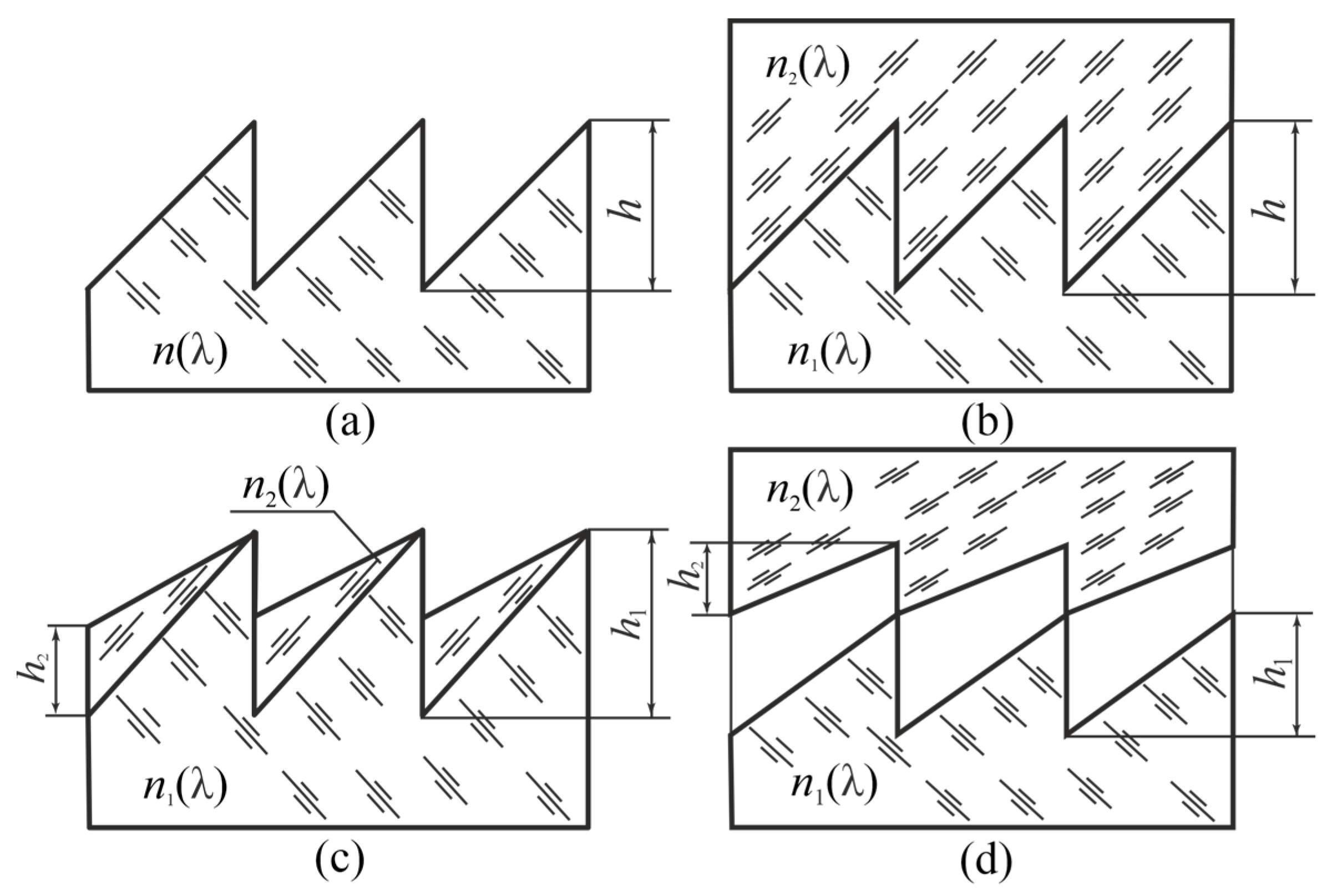
The maximum DE among the existing technologies for manufacturing ring quasi-periodic microstructures is provided by relief-phase microstructures. A single-layer microstructure (
Figure 1a) can have DE = 1, but only at one specific wavelength and for one specific angle of incidence of radiation, i.e., this microstructure has energy selectivity with regard to wavelength spectrum and angle of incidence. Two-layer, one- or two-relief microstructures have been successfully used to suppress spectral energy selectivity, as shown in
Figure 1b–d [
3,
4,
5,
6,
7].
The energy angular selectivity is more pronounced for two-layer microstructures than for single-layer microstructures; moreover, its minimization is ensured by minimizing the effective depths of the reliefs
heff (
heff =
h,
h1, and
h1 +
h2 in the schemes in
Figure 1b,
Figure 1c, and
Figure 1d, respectively). Assuming that the spectral energy selectivity is suppressed, the effective depths of the reliefs are minimized using an appropriate choice of pairs of optical materials in the microstructure arrangement.
Furthermore, the catalog of optical materials from which a pair of materials can be selected for a two-layer, single-relief microstructure, as shown in
Figure 1b, is significantly narrow, even in the visible range. This is because a material with a high refractive index should also have a higher Abbe number, a well-known requirement for pairs of materials with two-layer, single-relief microstructures [
4,
6]. If a certain number of such pairs, including heavy crown and light flint, are available from optical glasses, they are then completely absent from technological and commercially available optical plastics.
This limitation is eliminated due to the two reliefs made in the two optical materials with different dispersion properties. In addition, despite the obvious appeal (in terms of angular-energy selectivity) of a microstructure with one internal relief (
Figure 1c), in some cases, the choice may favor the microstructure shown in
Figure 1d. This primarily applies to infrared (IR) optics that operate over a wide range of temperatures. Indeed, owing to the different thermal coefficients of linear expansion of the two layers of the microstructure, as shown in
Figure 1c, ensuring mechanical strength at significantly different operating temperatures is impossible. Therefore, the most acceptable arrangement of the IR DOE microstructure currently is a two-layer microstructure with two internal sawtooth reliefs on the flat surfaces of the material substrates.
The search for optimal pairs of optical materials for the DOE microstructure is based on determining the optimal relief depths for each pair of optical materials; this requires multiple calculations of DE. As reported in [
8], the results obtained based on the DEs calculated using the scalar effective area method (EAM) [
9,
10] are fairly reliable in the layout and calculation of microstructures intended for operation in the IR and visible range [
9,
10]. This applies to a greater extent to selecting the optimal pairs of optical materials, but to a lesser extent to assessing the optimal depths of the reliefs and to assessing the achievable DE.
Indeed, the degree of reliability in determining the optimal depths and achievable DE depends on the given interval of angles of incidence of radiation incident on the microstructure for the selected relative (normalized to the total depth of the reliefs) spatial period of the microstructure P = Λ/(h1 + h2). Finally, these scalar results may be unreliable for microstructures with a total relief depth greater than the maximum wavelength of the working spectral range by an order of magnitude. The truly optimal relief depths of such microstructures, as well as microstructures designed for wide ranges of radiation incidence angles (±15° and more), and a reliable estimate of their DEs can only be obtained by optimizing in the framework of rigorous diffraction theory and solving the system of Maxwell equations. In this case, a good initial approximation is obtained using the scalar EAM method.
Currently, the most common numerical methods for solving systems of Maxwell equations to calculate DE are the rigorous coupled-wave analysis (RCWA) [
11,
12] and finite-difference time-domain (FDTD) methods [
9]. The insurmountable disadvantage of the latter method is that it requires considerably more computational time and computer RAM. Therefore, the RCWA method is preferred for calculating the DE of sawtooth microstructures. In particular, this method involves replacing the sawtooth relief of the diffractive microstructure with a set of flat lattice plates and applying a Fourier expansion to the periodically distributed permittivity of each plate. The accuracy of this method is determined by the optical thickness of the flat lattice slabs
L that make up both microreliefs and the number of modes
Nm. The computational complexity of the RCWA method depends on the aforementioned parameters.
The results of the RCWA analysis of the microstructures presented in this study are obtained using two software platforms developed with the participation of the authors of this paper, namely, PSUAC-DE [
13] and MC Grating Software [
14]. The PSUAC-DE algorithm is based on the enhanced transmittance matrix approach [
15] while the MC Grating Software algorithm does not differ from that proposed by Maharam [
11,
12].
Considering that in general, the DOEs of imaging optical systems operate with unpolarized radiation, DE calculation should include calculating the efficiencies for transverse electric (TE) and transverse magnetic (TM) polarized waves; moreover, the arithmetic mean of the obtained values is considered the resulting DE. However, in the practical calculation of the DEs of all types of microstructures as shown in
Figure 1, the computational complexity in the case of a TM wave is much greater, whereas the resulting efficiency values for TE and TM waves differ by no more than 2–3%, as confirmed in this study. Therefore, in this study, the efficiency calculated for the TE wave is considered as the DE obtained using the RCWA method.
However, even in this case, the duration of the computational process for calculating the DE of deep relief-phase structures (two-layer microstructures with two internal reliefs) may not be acceptable for optimizing the design parameters of the microstructure. To this end, this study proposes novel recommendations for selecting the values of the main computational parameters L and Nm to ensure the minimum computational time with guaranteed reliability of the calculation results.
2. Visible Spectral Range
One of the most pronounced signs of the inadequacy of the values of the computational parameters L and Nm in the target problem is the oscillation of the DE curves, showcasing the dependence of DE on the incidence angle of the radiation incident on the microstructure. Evidently, oscillations prevent not only the determination of the optimal depths of the reliefs, but also a reliable assessment of the maximum permissible angle of incidence.
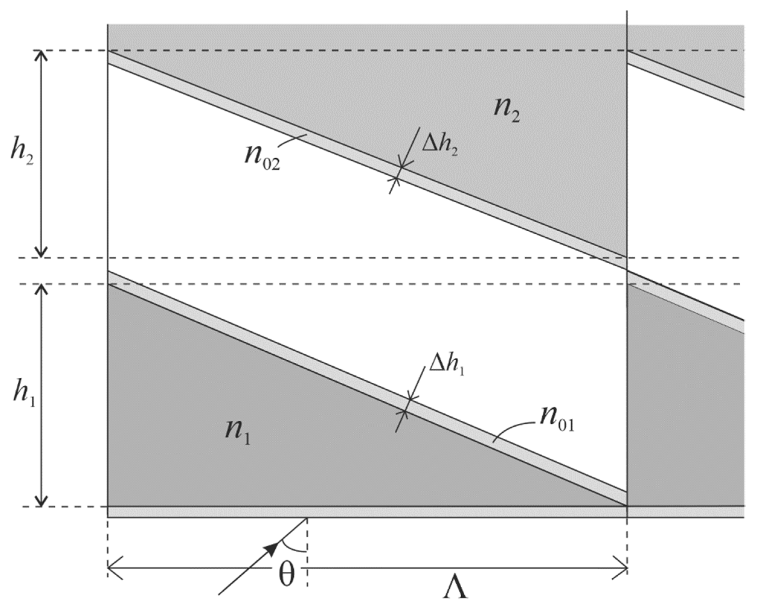
To clarify the causes of the oscillations and exclude the effect of Fresnel losses on the DE, antireflection coatings on the working surfaces of the microstructure are modeled into the calculation, as shown in
Figure 2.
The space between the reliefs in the microstructure materials with refractive indices
n1 and
n2 is filled with air; moreover, the sharp peaks of the reliefs are in contact with coatings with thicknesses of Δ
h1 and Δ
h2 and refractive indices of
n01 and
n02, respectively. The model coverage parameters for each wavelength are calculated using the following formulas:
where
i = 1, 2.
The calculations are performed for a microstructure [
7] with a lower layer of E48R crown-like optical plastic (
nd = 1.531160; ν
d = 56.0438) included in the ZEON catalog of the ZEMAX optical design software [
16] and an upper layer of EP7000 flint-like optical plastic (
nd = 1.651006; ν
d = 21.4946) manufactured by MITSUBISHI GAS CHEMICAL under the trademark, Lupizeta
TM EP7000 [
17]. The calculations are performed in the visible spectral range from λ
min = 0.4 µm to λ
max = 0.7 µm.
In the calculations, the radiation is assumed to be incident on the microstructure from the air onto the side of the medium with refractive index n1, the angle of incidence θ is measured from the normal to the substrate, and the diffracted radiation remains in the medium with refractive index n2. This is because the output of the diffracted radiation through a flat surface with a model antireflection coating would only increase DE calculation complexity without affecting the its results.
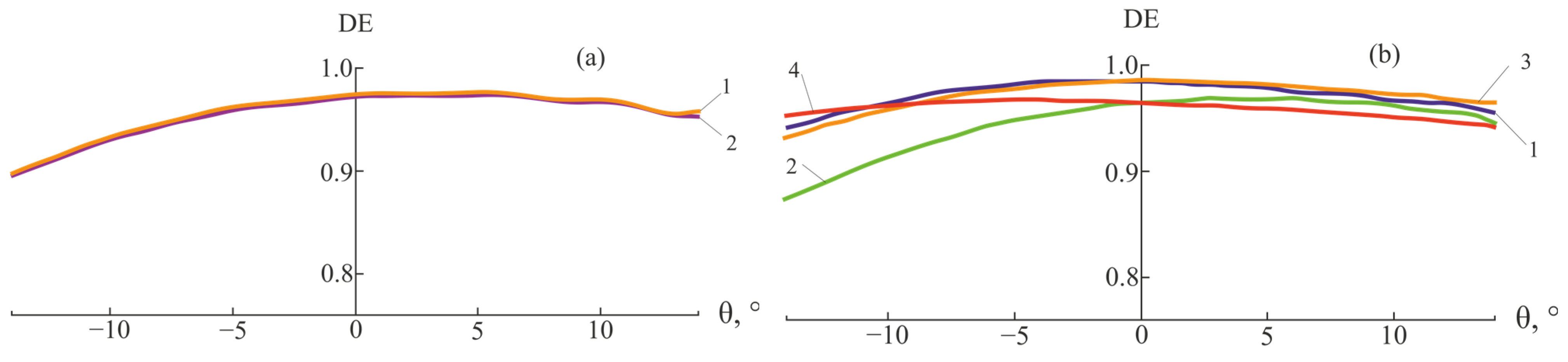
Figure 3 and
Figure 4 illustrate the dependence of DE on the angle of incidence obtained at two values of the relative spatial period of the microstructure
P = 10 and
P = 30. The number of plates in each of the two reliefs and number of modes
Np =
Nm = 200 ensured the absence of oscillations at
P = 30 and the fulfillment of the following condition:
Here, DEti and DEri are the diffraction efficiencies in transmitted and reflected orders, respectively. During the calculations, we considered all diffraction orders with numbers (1 − Nm/2) ≤ i ≤ Nm/2.
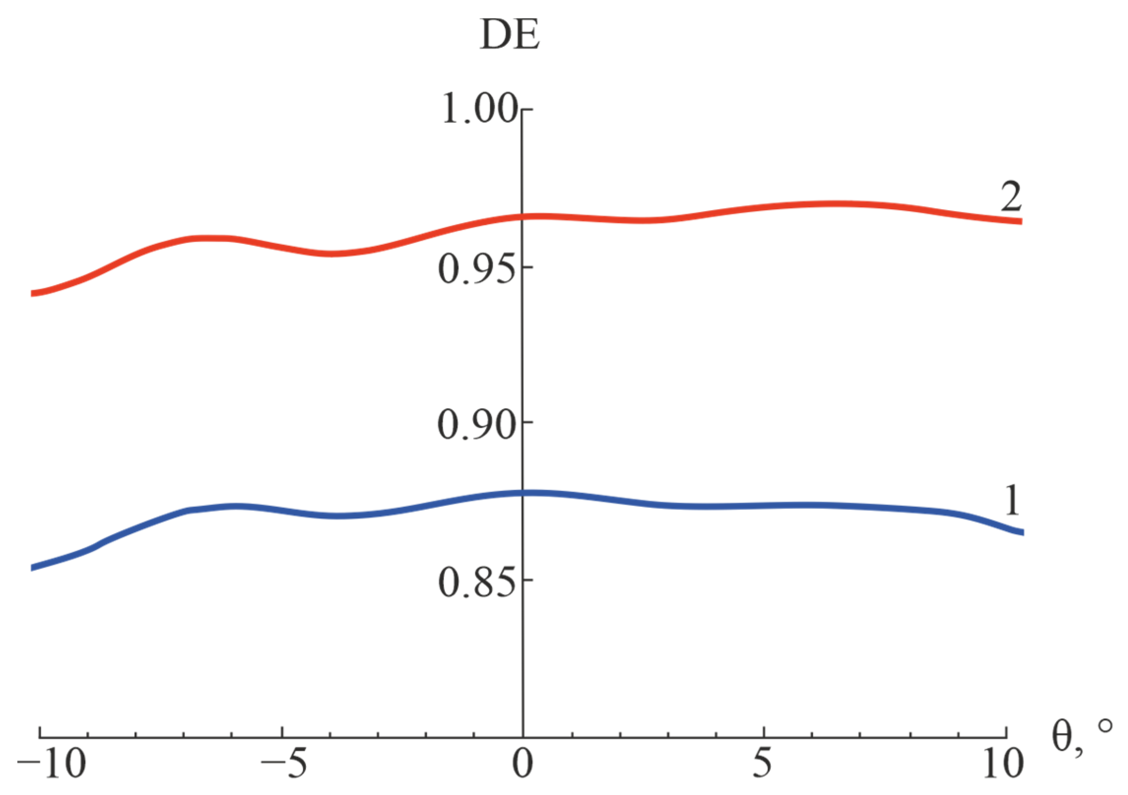
Considering that the oscillations are most pronounced at
P = 10 and λ = 0.7 µm, the calculation is performed with these parameters for the case without antireflection coatings (
Figure 4).
The calculation results presented in
Figure 3 and
Figure 4 confirm that the oscillating nature of the dependence of DE on the angle of incidence is not associated with the Fresnel reflection of radiation from flat or relief working surfaces of the microstructure; moreover, these dependences are identically retained even after almost completely suppressing the reflections. In particular, the oscillation amplitudes do not depend on the presence or absence of antireflection coatings, and the maximum oscillation amplitudes of curves 1,
An1, and 2,
An2, normalized by the constant component of DE are 0.72% and 0.65%, respectively.
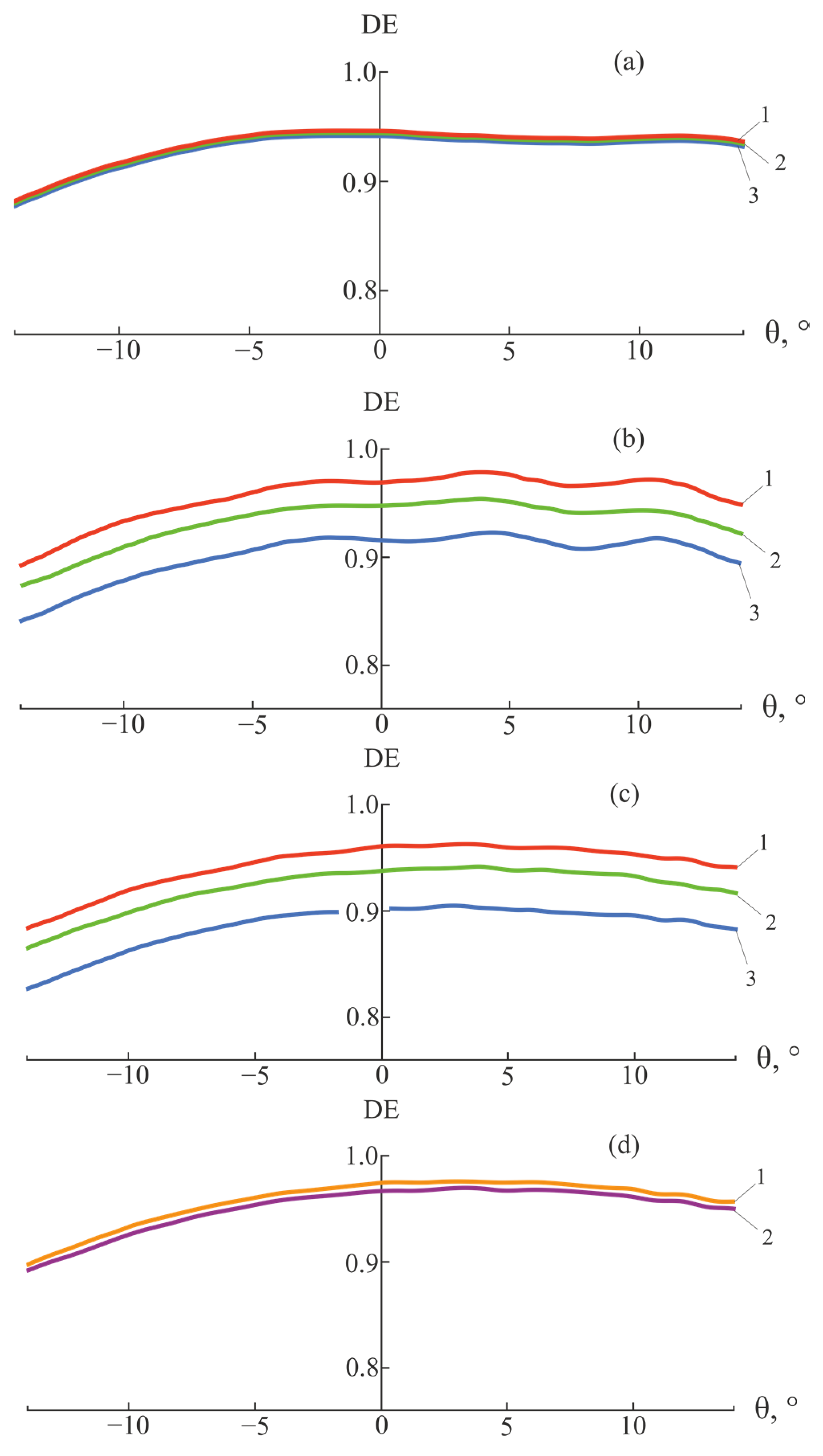
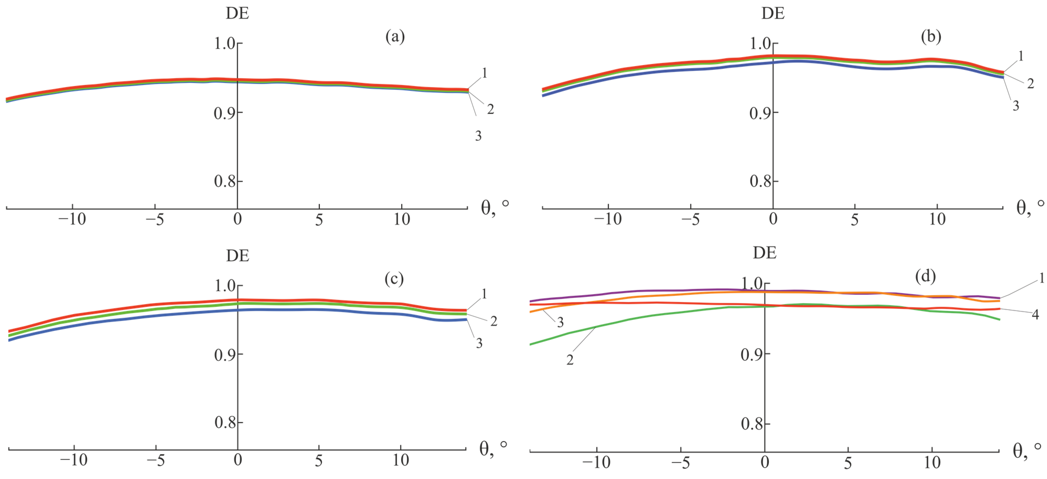
A novel, in-depth analysis of the influence of the parameters
L and
Nm on the level of DE and oscillations is presented next. Moreover, E48R/EP7000 microstructure with the model antireflection coatings is used for analysis. In this case, the optical thicknesses of the plates in both layers are assumed equal, i.e.,
L =
n1∙
lh1 =
n2∙
lh2 =
kλ. The analysis demonstrates that the optical thicknesses of the plates in the range of 0.08 ≤
k ≤ 0.32 have almost no effect on the oscillations, but significantly affect the DE level. Furthermore, the number of modes (50 ≤
Nm ≤ 600) affects both the DE level and oscillations. These trends are clearly confirmed by the graphs in
Figure 5 obtained at the central wavelength of the visible spectral range λ = 0.55 µm at
h1 = 8.792 µm,
h2 = 6.246 µm, and
P = 10. At
Nm = 50, the curves corresponding to all values of
k merge, and the DE level is the lowest (
Figure 5a). At
Nm = 200, the oscillations are pronounced (normalized oscillation amplitude
An = 0.53% at
k = 0.32), and the DE level increases with decreasing
k (
Figure 5b). At
Nm = 400, the oscillations decrease to an acceptable level, and the DE level, similar to that in
Figure 5b, increases with decreasing
k (
Figure 5c). A further decrease in
k leads to merging of the curves with a slight increase in the DE level and
An ≤ 0.07% at
k = 0.12 (
Figure 5d). Here, for all TE-polarization calculations, regardless of the values of
k and
Nm, condition (2) is satisfied. Therefore, a decrease in the DE in the first (working) diffraction order automatically leads to an increase in the DE in the side orders.
The calculation time increases with decreasing
k and increases depending on
Nm, usually according to a quadratic law. Accordingly, the maximum value of
k and the minimum value of
Nm can be used at which oscillations do not significantly affect the calculation results. In the case under consideration,
k ≤ 0.12 and
Nm = 300 at λ = 0.55 µm (
Figure 6a). Furthermore, at other wavelengths of the working spectral range, the oscillations can have a slightly larger amplitude, requiring a decrease in
k to 0.08 and an increase in
Nm to 400 for their almost complete suppression (
Figure 6b).
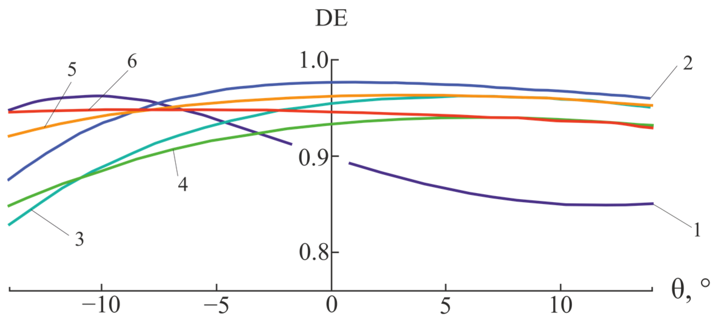
A double increase in the relative spatial period of the microstructure (
P = 20) does not affect the recommended value of the
k parameter (
k ≤ 0.12), but requires an increase in the recommended value of the
Nm parameter (
Nm ≥ 500, see
Figure 7). Indeed, at
Nm = 400 and 600
An ≤ 0.068%, and
Nm ≤ 0.043% (in both cases
k = 0.16).
Comparing the recommended
Nm values obtained for this microstructure at
P = 10 and
P = 20, the following simple relation is valid:
where λ is the central wavelength of the working spectral range.
Note that, as pointed out in [
7,
18], an increase in the spatial period of the microstructure allows expanding the range of radiation incidence angles within which the DE does not fall below a given level.
Similar calculations for two-layer microstructures with two internal sawtooth reliefs composed of pairs of optical plastics, namely, PMMA/POLYCARB, E48R/POLYSTYR, and E48R/ITO in PMMA [
7] result in the same recommended
k and
Nm values. Moreover, this does not depend on whether PSUAC-DE or MC Grating Software is used for calculations.
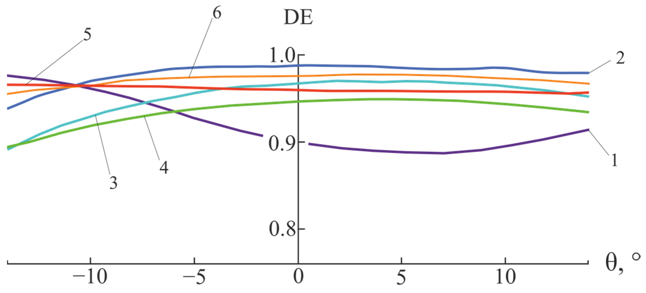
Furthermore, we present one of the typical results of calculating DE for two cases: TM and TE polarization. This calculation was performed for the E48R/EP7000 microstructure at
P = 10 and
k = 0.32 at a wavelength λ = 0.55 μm over three angles of incidence of radiation θ = 0° and θ = ±14°. The increase in computational complexity for TM polarization is associated not so much with an increase in the required number of
Nm modes taken into account, as with the need to select the
Nm value to fulfill condition (2) (see
Table 1).
The data in
Table 1 show that with optimal selection of the number of modes for each angle of incidence of radiation, the difference in the DE values calculated for the TM and TE polarizations does not exceed 2.6%. However, this results in a significant increase in computational complexity.
3. Infrared Spectral Range
In this section, we investigate how the optical thickness of the plates L and the number of modes Nm influence the relationship between the DE of microstructures and the angle of incidence of IR radiation. These microstructures belong to the DOEs of several refractive-diffractive objectives designed by the authors of this article. The objectives were designed to operate in the dual IR range, including medium-wavelength IR (MWIR) (3.4–5.2 µm) and long-wavelength IR (LWIR) (7.5–11.4 µm) subranges.
The results of the study are demonstrated by the example of two microstructures, SRF2/GERMANIUM (
h1 = 53.6 µm and
h2 = 8.71 µm) and PBF2/GASIR1 (
h1 = 87.36 µm and
h2 = 44.12 µm). Three materials of their layers (SRF2, PBF2, and GERMANIUM) are obtained from the INFRARED catalog of the ZEMAX program; moreover, GASIR1 is obtained from the UMICORE catalog [
19]. The choice of these microstructures is not accidental. They both have a fairly high DE at |θ| ≤ 14°, whereas the refractive indices of the respective layers differ by more than 1.2 and 1.6 times (
Table 2).
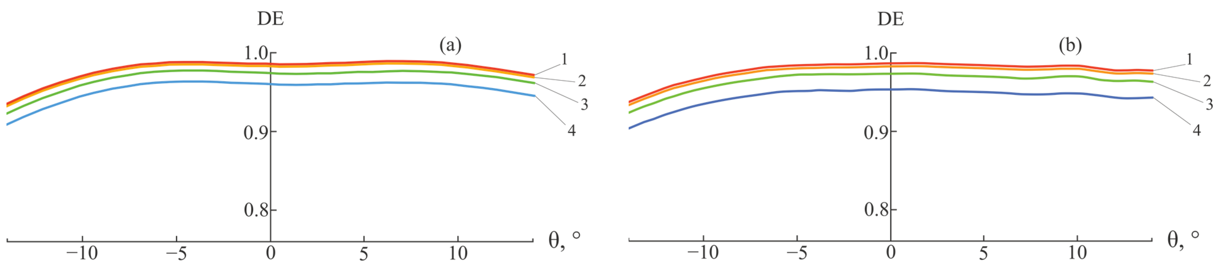
In the calculations, as in the visible range, the radiation is assumed to be incident on the microstructure from the air onto the side of the medium with the refractive index n1, the angle of incidence θ is measured from the normal to the substrate, and the diffracted radiation remains in the medium with the refractive index n2. In this case, the optical thicknesses of the plates in both layers are assumed equal, i.e., L = n1∙lh1 = n2∙lh2 = kλ.
Figure 8 shows the dependence curves of the DE for the SRF2/GERMANIUM microstructure with regard to the angle of incidence, obtained using PSUAC-DE program at
P = 10.
At
Nm = 200, the oscillations are insignificant (
An ≤ 0.06% at
k = 0.1), whereas at
Nm = 400, they disappear completely. In this case, a
k value of less than 0.05 does not make sense. This is true for all dual-IR wavelengths (
Figure 9).
A two-fold increase in the relative spatial period of the microstructure in this case does not affect the recommended value of the parameter
k, but requires an increase in the number of modes to reduce the oscillation amplitude to an acceptable level (
Figure 10 and
Figure 11).
By comparing the
k values used in the visible and IR ranges as well as the refractive indices of E48R/EP7000 and SRF2/GERMANIUM microstructures, the following empirical formula is proposed for the relationship between the corresponding
k values:
where
kIR and
kVis are the
k parameters of the second layer of the microstructure at the central wavelengths of the MWIR and visible ranges, respectively. Similarly,
n2(IR) are
n2(Vis) are the corresponding refractive indices.
An analysis of the influence of the
k and
Nm parameters on the level and oscillations of the DE of PBF2/GASIR1 microstructure is conducted at the values of
k calculated using Equation (4). The results for
P = 10 case are presented in
Figure 12.
An increase in the relative spatial period of the microstructure to P = 20 does not affect the recommended value of the parameter k in the case of this microstructure; however, a two-fold increase in the number of modes is required, which reduces the oscillation amplitude to an acceptable level.
Note that in the IR and visible ranges, an increase in the spatial period of the microstructure allows expanding the range of radiation incidence angles within which the DE does not fall below a given level.
Summarizing the results presented in
Section 2 and
Section 3, the value obtained via Equation (3) should be considered as the recommended number of modes for all microstructures in both the visible and IR ranges. As for the parameter
k, based on Formula (4), it should be taken as its recommended value
k ≤ 0.264/
n2, where
n2 is the larger of the two refractive indices of the microstructure layers at the central wavelength of the visible or MWIR ranges.
Obviously, an increase in the relative spatial period, which allows the expansion of the range of angles of incidence of radiation incident on the microstructure, inevitably increases the computational complexity of the RCWA calculation of the DE.
5. Conclusions
The DOE of imaging optical systems in both the visible and IR ranges must have a high DE within the working spectral range and within a given range of angles of incidence of radiation incident on the microstructure. These requirements are satisfied, in particular, by the elements with a sawtooth two-layer two-relief microstructure. In this case, a reliable and optimal pair of optical materials for such a microstructure can be selected within the framework of the scalar theory of diffraction. However, truly optimal relief depths and a reliable assessment of the DE level of the microstructure within a given range of radiation incidence angles can be obtained, in most cases, only as a result of electromagnetic optimization, particularly using the RCWA method. The accuracy of this method is determined by the optical thicknesses of the flat lattice slabs L = n1∙lh1 = n2∙lh2 = kλ that make up both the microreliefs and the number of modes Nm, i.e., the harmonics of the Fourier series. The computational complexity of the calculations also depends on these parameters.
The recommendations proposed and substantiated in this study on selecting the number of modes and optical thickness of the plates (Equations (3) and (4)) allow the minimization of the computational complexity of the RCWA calculation of the DE of a sawtooth two-layer two-relief microstructure while maintaining the specified reliability of the calculation results.
Moreover, the computational complexity can be controlled through the relationship Nm = CΛ/λ, i.e., by allowing one or another level of oscillation of the DE curves, depending on the angle of incidence. By setting C ≤ 1, the complexity of multiple DE calculations can be reduced in the optimization process. Moreover, by setting C > 1, the computational complexity can be increased to certify the accuracy of the solution obtained as a result of implemented optimization.

 ,
, 


