Article

The Design of Large Curved Waveguide Based on Sunflower Graded Photonic Crystal

1
School of Electronic Engineering, North China University of Water Resources and Electric Power, Zhengzhou 450046, China
2
Henan Key Laboratory of Laser and Opto-Electric Information Technology, School of Information Engineering, Zhengzhou University, Zhengzhou 450052, China
*
Authors to whom correspondence should be addressed.
Photonics 2023, 10(7), 781; https://doi.org/10.3390/photonics10070781
Submission received: 8 March 2023 / Revised: 18 June 2023 / Accepted: 2 July 2023 / Published: 5 July 2023

Abstract

:
In this paper, three large curved waveguides based on Sunflower Graded photonic crystal are designed. Numerical simulations of electromagnetic beam bending in Sunflower Graded photonic crystals have shown that homogenization based on the Maxwell–Garnett theory gives very good results for steering the electromagnetic field. In contrast to the progressive bending waveguide structures based on periodic photonic crystal designs reported in the literature, this structure is not only simple in design, but also the optical wave trends in the progressive bending waveguide structures are more smooth. Sunflower structures, due to their high circular symmetry, have a great advantage in making arbitrary curved waveguides. The results have some theoretical implications for the design of optical integrated circuits and the selection of optically thin communication devices. It is also useful for the selection of meta-materials.

1. Introduction

The photonic crystal (PC) was independently proposed by John S. [1] and Yablonovitch E. [2] in 1987. It is an artificial microstructure formed by periodic arrangement of media with different refractive indexes. In terms of material structure, A PC is a kind of man-made crystal with periodic dielectric structure on the optical scale. PCs and semiconductors have many similarities in basic models and research ideas. In principle, people can control the movement of photons by designing and manufacturing PCs and their devices. In general, the lattice period, the index of refraction, and the filling rate of each material in the PC unit cell are constant. Therefore, the band structure remains the same as in the case of stable optical properties. The concept of Graded Photonic Crystals (GPCs) was introduced in Refs. [3,4], in which one or more of the above three parameters (cell size, refractive index, filling ratio) of a PC are subjected to continuous and slow changes, thus forming a new PC structure. In principle, the dielectric structure with arbitrary refractive index distribution can be realized by reasonably controlling these three structural parameters. The main application areas fall into two categories [5]. One is used as self-focusing lens, such as a Lambert lens and a negative refraction lens to realize the focusing, collimation, coupling, imaging, and Fourier transform of light beams. The other is used as a beam deflector to realize the beam’s super displacement and super turn, transform optical elements, electromagnetic stealth, and so on. Guiding light in inhomogeneous PCs using, not the existence of a photonic band-gap, but a well-designed spatially dependent dispersion was proposed in Refs. [6,7]. The curved wave-guide can connect non-collinear optical components and change the propagation direction of the beam, especially the small size and low loss curved wave-guide, which can improve the integration of integrated optics and reduce the device size and cost [8]. Zhou et al. [9], from Southeast University, made a 90-degree bend structure using artificials, following the theoretical work on arbitrary waveguide bends using gradient-index and isotropic materials. Vasić B et al. [10] described devices which could bend the propagation direction and squeeze the confined electromagnetic fields. They also investigated possible realization of isotropic gradient refractive index media at optical frequencies using two-dimensional graded photonic crystals [11].The gradient bending 90-degree waveguide structure was based on the tetragonal photonic crystal lattice. In order to minimize the energy loss, the gradient structure had more than 30 layers. Scheuer et al. [12] numerically calculated that a resonator with a high quality factor could be realized by the circular ring photonic crystal structure. Derek et al. [13] optimized the structure by using coupled wave theory to improve the quality factor of the resonator. Of course, for tuning the light transmission of photonic crystals, besides the variation of structure design, another essential means is the online tuning with a liquid-filled photonic crystal [14,15]. Kamau S et al. studied high light absorption in two devices: a stack of Au-pattern/insulator/Au-film and a stack of Au-pattern/weakly-absorbing-material/Au-film, where the Au-pattern was structured in graded photonic super-crystal [16]. Pendry J B et al. show how electromagnetic fields can be redirected by using the freedom of design that meta-materials provide and worked on the cloaking of objects from electromagnetic fields [17]. With the development and maturity of nano-materials, meta-materials have become a hot topic of research in recent years. Meta-materials are artificial composite structures or composite materials that have non-trivial physical properties that natural materials do not have. Meta-materials are artificial electromagnetic materials consisting of artificial sub-wavelength resonant units arranged according to periodic or quasi-periodic arrangements. Since the size of the resonant unit structure of meta-material is considerably smaller than the working wavelength of electromagnetic wave, these resonant units can be equivalent to uniform electromagnetic medium, in a sense, so that the electromagnetic wave can be regulated by designing the resonant unit to achieve an arbitrary dielectric constant and permeability. Due to the drawbacks of 3D meta-materials, such as extreme losses, strip widths, and fabrication difficulties, researchers have gradually turned their attention to 2D meta-materials, known as meta-materials. Currently, meta-surfaces have demonstrated their superiority in anomalous reflection/refraction, polarization conversion, and super-absorption. In addition, photonic crystal, as a kind of artificial structure meta-materials, also provides a powerful means to manipulate electromagnetic waves [18]. Savotchenko S E discovered a different type of surface wave characterized by a linear gradient index of dielectric constant mutation and propagated by an intensity-dependent refractive index layered structure. They found that the characteristic distance and effective refractive index of the gradient index medium can control the redistribution of wave energy between the semiconductor layers [19]. Hassan et al. developed graded photonic super-crystals to show an enhanced light absorption and light extraction efficiency when they are integrated with a solar cell and an organic light emitting device, respectively [20]. Badri S H et al. presented a low-loss and compact 90° waveguide bend with a radius of 9 μm designed by truncating the Eaton lens, and they evaluated the performance of the designed bend, which was implemented by graded photonic crystal through the full-wave two-dimensional finite element method [21]. Zhang H et al. constructed full-dielectric planar nanostructures of gradient topological photonic crystals by changing the degree of lattice shrinkage and expansion, which has the advantages of low loss, robustness, and easy integration [22]. Xiao [23] et al. also set a defect mode for this structure and improved the quality factor of the resonator, making its Q value greater than 105. At the same time, they also studied the waveguide of the structure, reporting the transmission properties of the circular photonic crystal. It was found that, compared with the traditional photonic crystal waveguide structure, the transmission bandwidth and bending loss of the circular photonic crystal were significantly improved. On the other hand, the Sunflower quasi-periodic photonic crystal structure has significant advantages in the design of waveguides with different degrees of bending, which is easier to achieve in circular structures [24].
The analysis of the Sunflower QPC has shown its incomparable advantages in the fabrication of large curved waveguides and lenses due to its excellent circular symmetry, but there have been few reports of such structures. In this paper, we design a large curved waveguide based on the Sunflower QPC and compare and analyze different designs to provide more useful reference values.

2. The Principle of the Design

The Sunflower quasi-periodic photonic crystal (QPC) is aperiodic, but the dielectric column is systematically distributed on an air background. The spatial lattice positions in the x − y plane are given by
x = a N cos ( 2 m π M N ) , Z = a N sin ( 2 m π M N ) ,   m = 1 ~ MN
where a is the distance between two adjacent circles as the lattice constant which is defined as the radial periodicity, N is the ordinal number of each circle from inside to outside, M is the number of dielectric columns in the first ring, m is the variable, and x, z are the coordinates of each medium column. Six-weight Sunflower structures were mainly studied in, so M = 6 was substituted into this formulation.
In this work, to facilitate the investigation, a typical Sunflower PC with a = 0.1 μm is adopted, which consists of Si dielectric rods (εr = 11.6) embedded in air media (εhost = 1). A schematic diagram of the sunflower structure is shown in Figure 1.
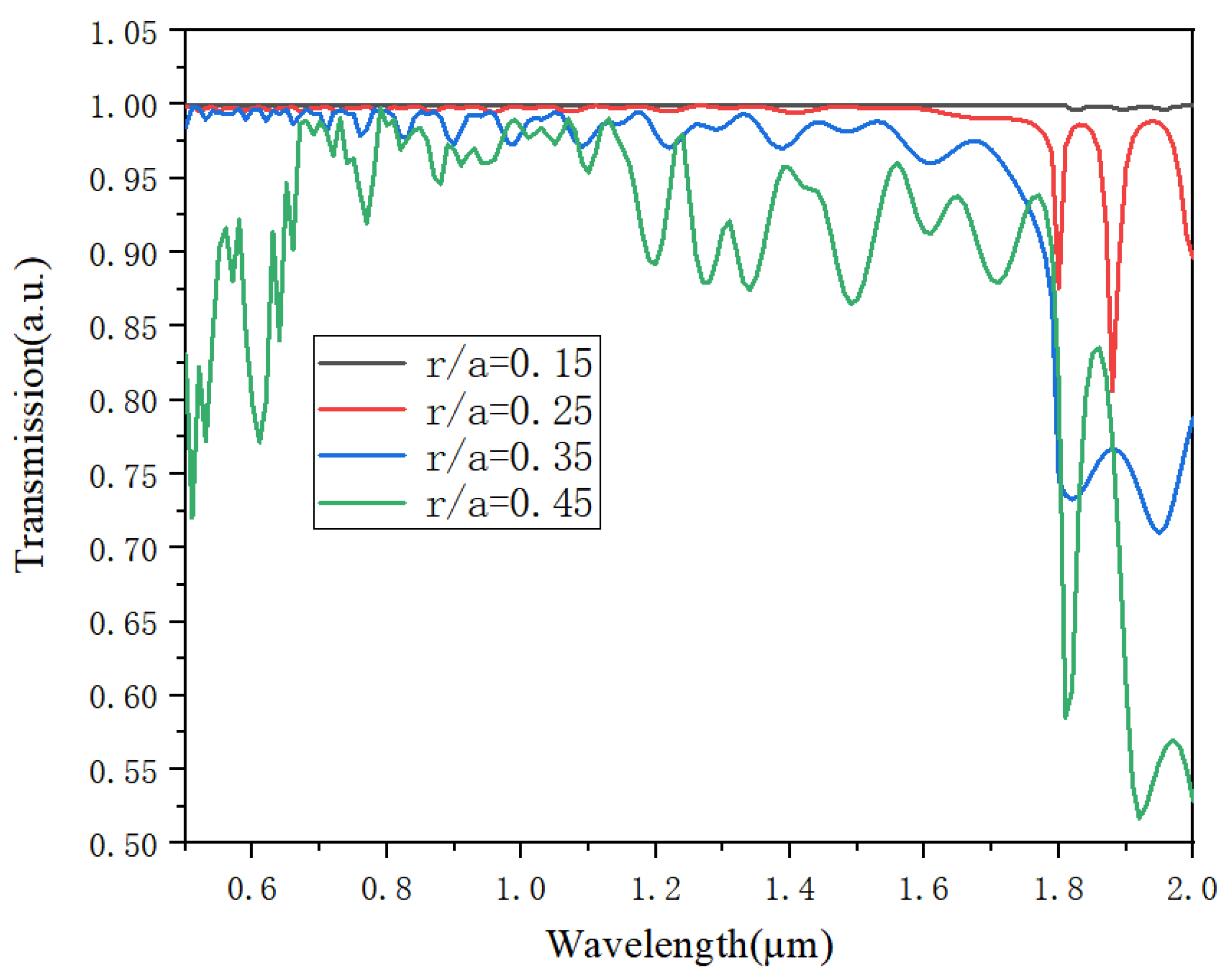
The transmission spectra of such PCs are calculated at different filling fractions, since the first Brillouin zone and the isophotal plane describing the negative refraction effect are not present in quasi-periodic photonic crystals, whereas the photonic band structure is easily accessible. The Sunflower QPC also has no usable equivalent surface. Therefore, the transmission bandwidth beyond the band gap can be explored for any quasi-periodic Sunflower photonic crystal structure. Figure 2 shows the transmission bandwidth at different filling factors r/a. In Figure 2, the plane-wave expansion method is used for the calculations. In this work, The DIF-FIRACTMOD module is mainly used in the theoretical basis of the plane-wave expansion method to scan the transmission spectrum at 0–3 µm wavelengths, so the transmission spectrum is roughly calculated. The calculations in this figure are for reference only. We chose wavelengths with large transmittance to calculate the light field distribution.
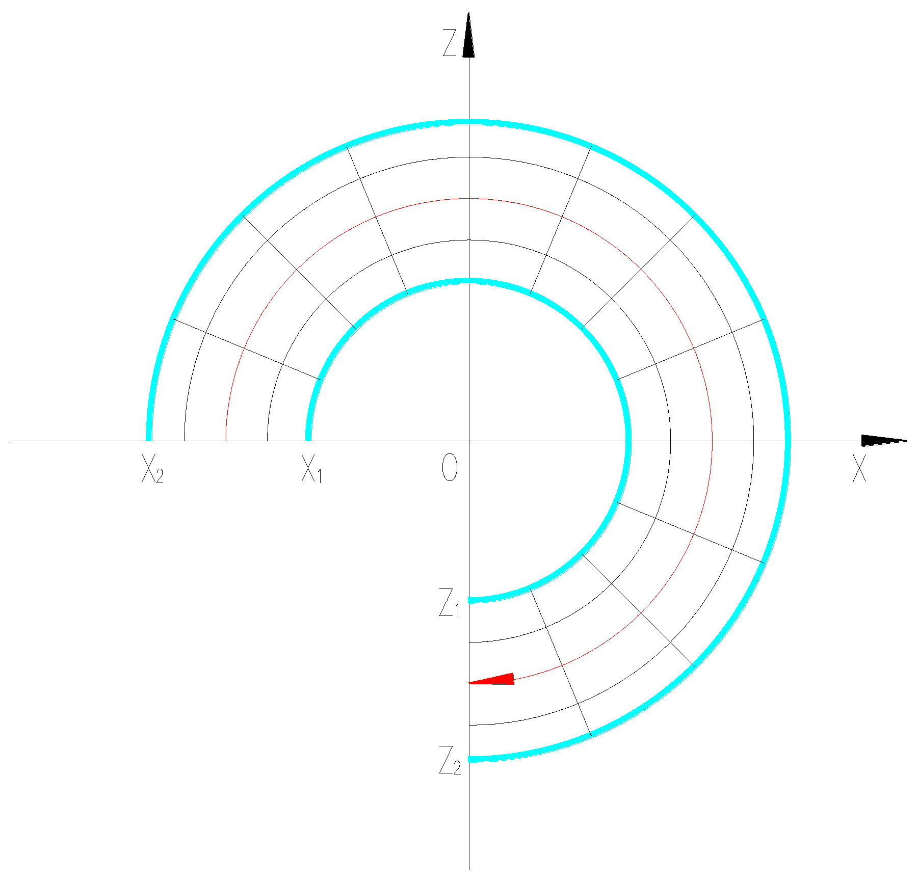
The engineering of the refractive index profile is a useful method for controlling the electromagnetic field. Gradient photonic crystals are able to control the direction of light propagation and bend light waves. Thus, graded photonic crystals can also be theoretically fabricated as large curved waveguides, and their model is shown in Figure 3.
The following formula is used for the refractive index distribution [7]:
n = C/ρ
The constant C can be used to tune the dielectric profile within the bend. n is the refractive index of lens, and ρ is the distance between the dielectric column and the dot. The refractive index n depends largely on the coordinate ρ. Based on the Maxwell–Garnett theory, the analytical formulas are given for calculations of the rods radii, which makes the implementation straightforward [11]. According to the Maxwell-Garnett effective medium theory, the effective refractive index of a graded photon crystal is given by
ε x = ε y = ε p l a n e = ε h o s t = ε h o s t + f ε h o s t ( ε r o d s ε h o s t ) ε h o s t + 0.5 ( 1 f ) ( ε r o d s ε h o s t )
ε z  can be obtained from the following formula
ε z = ( 1 f ) ε h o s t + f ε r o d s
The filling factor of the dielectric column is determined by the formula f = Nπr2/S. S is the area of the lattice structure, N is the number of dielectric columns in the lattice, and r is the radius of the dielectric column. Area S = 0.5 a 2 sin ( π / 3 ) and N = 0.5; hence, the filling factor is f = π r 2 / a 2 sin ( π / 3 ) . According to Formula (2), the magnitude of n depends on the coordinates of the medium column ρ, where f is the filling ratio of the dielectric column, ε h o s t is the dielectric constant of substrate medium, ε r o d s is the dielectric constant of dielectric column, and the effective refractive index of the structure is n t e = ε p l a n e , n t m = ε z .
Therefore, in the TE polarization mode, the radius of r t e is
r t e = S ( ε h o s t n 2 ) ( ε r o d s + ε h o s t ) π N ( ε h o s t + n 2 ) ( ε h o s t ε r o d s )
In the TM polarization mode, the radius of r t m is
r t m = S ( ε h o s t n 2 ) π N ( ε h o s t ε r o d s )
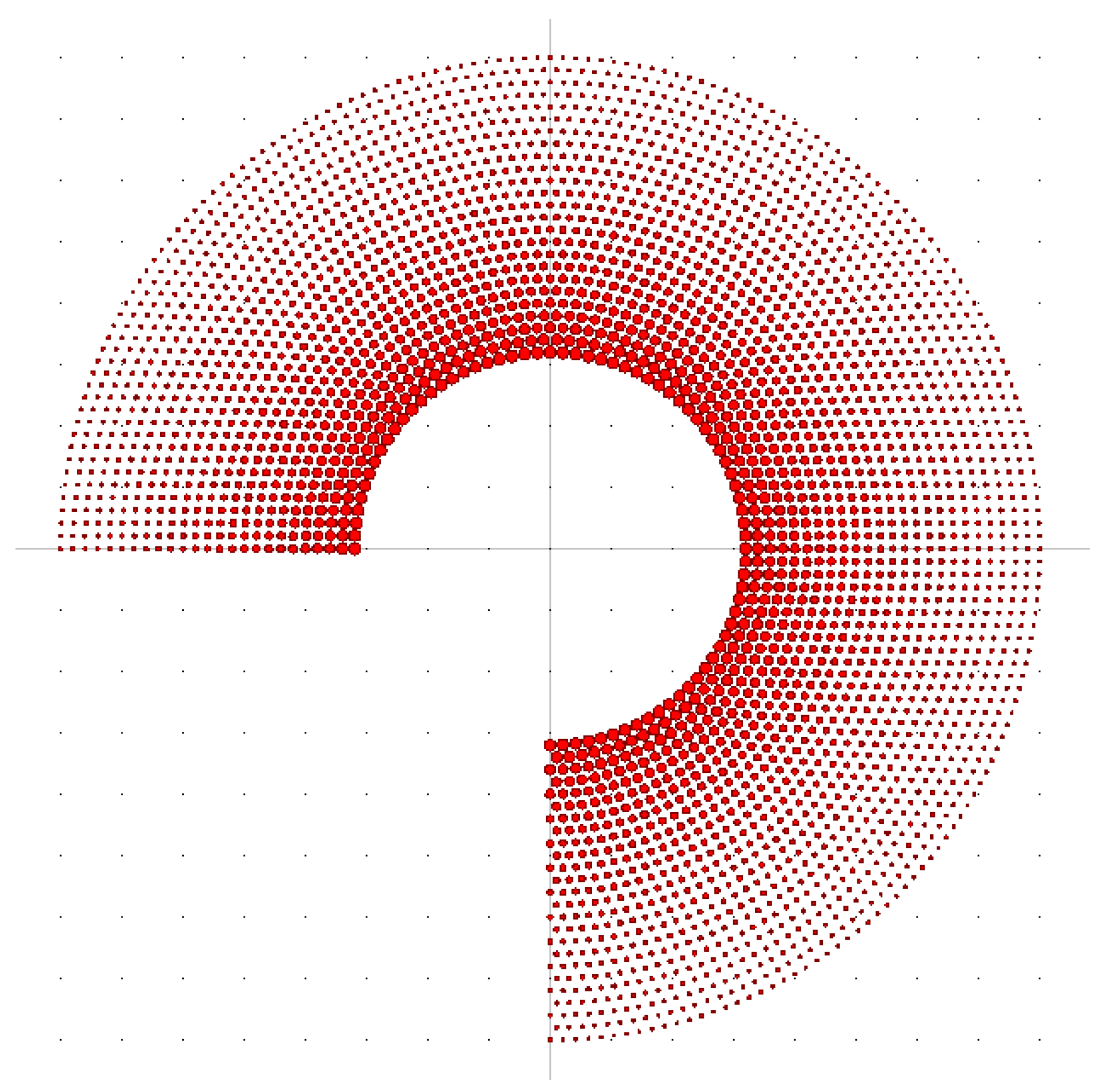
According to reference [24], Sunflower gradual photonic crystal has a better light propagation effect of TM type than TE type; therefore TM type is directly selected here. The basic structure is a 4 µm by 4 µm circular photonic crystal lattice of elevated index rods n = 3.4 in an air background n = 1, with the lattice constant a = 0.1, which is based on the reference [24]. In order to improve the contrast between the refractive index of the cladding and the core of the bent waveguide, and to reduce the radiative losses of the bent waveguide, high refractive indices are usually used. Compared with low refractive index contrast materials, HIC materials offer advantages such as thinner waveguide core thickness and smaller bending radius. However, nonlinear effects can be mitigated by using high-quality waveguide materials and optimizing the waveguide structure design. According to the reference [25], the appropriate transmittance wavelength is calculated. ρ is the distance between the dielectric column and the center of the circle. According to the calculation, the effective point coordinates from the center of the circle are 1.6~4.0 µm, and the corresponding refractive index is 3.12~1.25. The radius of each circle of the media column was calculated according to an equation, as shown in Table 1. The Sunflower gradient waveguide structure model is designed based on Table 1 and is shown in Figure 4.

3. The Simulation of Large Curved Waveguide

The simulation calculation uses the Fullwave module based on FDTD theory; the mesh size is 0.005 µm, and the time step is half of the mesh. The boundary adopts a perfect matching layer. A light source with coordinates x = 1.85 µm and z = 0.2 µm is vertically incident from the left port of the device in a continuous Gaussian light wave. The construction for the constant C = 5 is first computed. The C = 3 structure is then calculated and compared to the C = 7 structure. Light field simulations were performed on the structure shown in Figure 4. Three communication wavelengths of 0.85 µm, 1.31 µm, and 1.55 µm were selected for light field simulation, as shown in Figure 5.
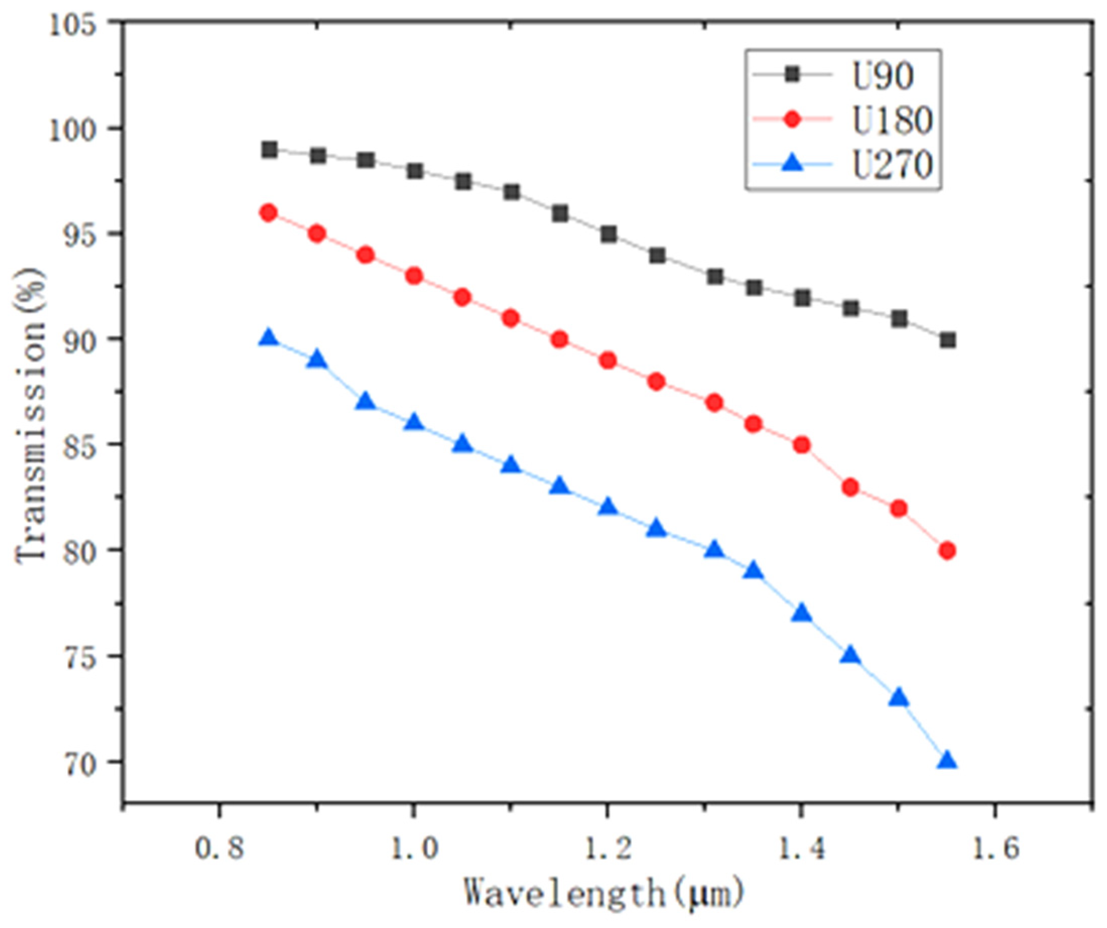
As can be seen from Figure 5, beam splitting appears in the graded waveguide structure. Due to the large refractive index near the center, the light wave passing through here is sharply bent, whereas, in the outer ring structure, the light wave is slowly bent due to the small refractive index, which eventually leads to the apparent escape of the light wave in the outer ring. According to this phenomenon, the structure can be reduced from the outer loop to the middle to achieve better results. Based on this principle, the structure is compared and optimized. When the distance between the inner ring and the center of the circle is 1.6 µm and the outer ring is 2.1 µm, a better guided wave structure can be found. At this time, the corresponding refractive index ranges from 3.12 to 2.38. The detector is placed at the structure bending 90 degrees (U90), bending 180 degrees (U180) and bending 270 degrees (U270). The calculated wavelength and transmittance are then shown as follows.
As can be seen from Figure 6, with the increase in bending degree and the extension of the bending path, the energy loss increases significantly, and the corresponding transmittance inevitably decreases. For integrated optical WDM devices, it is generally sufficient to use only 90° curved waveguides. As shown in Figure 6, when the waveguide is bent within 90 degrees, the loss is very low, and the structure has a high transmittance, all of which are above 90%. Although in terms of structure fabrication, defective waveguides have more flexible and simple fabrication methods than graded waveguides. However, this structure still provides a more selective idea for the selection of future integrated devices. In this manuscript, we artificially control the wavelength in the visible band to design the structure. Based on the normalized frequency formula ν = a/λ, it can be seen that a and λ are positively correlated, and, using this relationship, the structural design parameters can be arbitrarily changed according to the wavelength. In addition, it can also be seen from Figure 6 that, with the increase in wavelength, the transmittance also decreases correspondingly. From the light field distribution diagram in Figure 7, it can also be clearly seen that long-wavelength light waves have more energy leakage during the propagation process. For the models with high curvature, the future applications are mainly considered from the direction of meta-materials. This paper mainly studies its ability to manipulate electromagnetic fields. When C = 3 or C = 7, large curved waveguides can be calculated and compared using the same method. The coordinates and radii of C = 3 and C = 7 can be computed in the same way. Here, only the useful data are shown in Table 2 and Table 3 as follows.
Figure 8 and Figure 9 show the light field map of its transmission performance. For C = 3, the inner diameter of the gradient waveguide is 1 µm. It can be observed from Figure 8 that the transmittance is high at short wavelengths, but the energy loss is largely at long wavelengths. Based on the data in Figure 10a, it can be concluded that the transmittance drops steeply for wavelengths larger than 1 µm, and approaches 0 for wavelengths up to 1.5 µm. This phenomenon can be explained by the dispersion principle of light. The dielectric columns that make up the large curved waveguides of photonic crystals resemble lenses. The larger the λ is, the smaller the refractive index is. Thus, for large wavelengths, the smaller refractive index leads to a poor bending efficiency. At wavelengths larger than 1 µm, the transmittance drops dramatically. At 1.5 µm, the transmittance approaches 0 because the light wave is already scattered out of the structure before it bends towards the end point.
For C = 7, the inner diameter of the gradient waveguide is 2.2 µm. It can be observed from Figure 8 that the entire waveguide has excellent transmission. Combining with the data in Figure 10, the whole waveguide could maintain more than 90% transmission when the waveguide curvature is less than 180°. The transmittance is also above 80% at 270 degrees of bending.

4. Robustness Analysis

David L et al. reported that the gradient photonic super-crystals and the gradient photonic super-crystals with two periods and two bases dependent on position were synthesized by holography combined with a spatial light modulator and a single reflecting optical element [26]. The fabrication of 3D photonic crystals has been reported in the relevant literature. For example, Lin et al. reported the holographic fabrication of three types of 3D GPSCs through nine beam interferences and their characteristic diffraction patterns [27]. Qi Y et al., according to the structure, selected different exposure thresholds and background materials, and they used the multi-beam interference method to design and experiment to obtain the photon structure with gradient intensity distribution [28].
By searching references, we find that most of them use multi-beam interferometry for the production of hierarchical photonic crystals. The above, however, is based on periodic photonic crystals. For such aperiodic photonic crystals, no better production method has been found so far by reference to data. There is only one way to fabricate such structures: the electron beam exposure. Electron beam exposure is a technique in which an electron beam is used to directly trace or project a photocopy image onto a wafer coated with a photoresist adhesive. It features high resolution, easy to produce and modify graphics, and a short production cycle. When it comes to processing, it is necessary to consider the fault tolerance of the system.
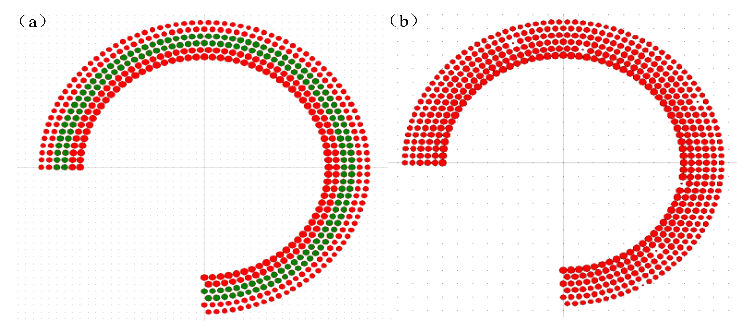
As a reference to the preparation process, the following model is constructed to demonstrate that the fabrication of these structures could be not rigorous, and imperfections are allowed. Figure 11a shows the model in which two adjacent layers of rods keep the diameter unchanged and do not obey the GRIN rules for the waveguide. The green bars mark the regions with imperfect gradients, corresponding to layers 3 and 4 of the waveguide. Figure 11b shows the model in which a point defect occurs at any random position in the circle.
By calculating the photonic crystal curved waveguides with imperfect gradients and the photonic crystal gradient waveguides with defective gradients, we found that the results do not change significantly when compared to the perfect gradient structures. The resulting discretization of the light field is shown in Figure 12 and Figure 13.

5. Application Prospect Analysis and Prospect

At present, integrated optics research is in a period of rapid development and plays an influential role in social development. In integrated optics, waveguides connect different optical components to enable light transmission. Waveguides can be divided into curved and straight waveguides depending on their geometry [8]. The curved waveguide can realize the connection of non-collinear optical components and alter the propagation direction of the beam [29]. Bending is an essential component of integrated optical waveguides and is one of the hot research topics. After years of development, the transmission efficiency of curved waveguides has been improved, and it has been used in several fields of integrated optics. The curved waveguide could be connected to the straight waveguide to achieve the beam deflection. Due to the different radius of the curvature of the connection between the straight and curved waveguides, the center of the mode field of the straight waveguide does not coincide with the center of the mode field of the curved waveguide, and the center of the mode field is shifted outward to some extent. Thus, if the straight and curved waveguides are directly connected, the mode conversion loss is induced. Neumann [30] and others analyzed the fact that the center mode field does not match the phenomenon put forward on the straight and bent waveguides in the structure of joint design, which has a certain offset (as shown in Figure 14b). The purpose is to reduce, because the straight and bent waveguide mode field locations in the heart pattern do not match the transmission loss caused by [31]. Offset structure can effectively reduce losses caused because the pattern does not match [32], but, for photolithography and etching, it has superior precision requirements.
We translated the incident light wave image by 0.3 to the left, as shown in Figure 14d, and its light field distribution is shown in Figure 14e. It was found that, even if the center position of the incident mode field is shifted, the results were still not significantly affected for such a gradual structure. This scheme can effectively avoid the loss caused by the mode mismatch problem. It is well known that curved waveguides with small sizes and low losses can improve the integration of integrated optics.
Also, this reduces the device size and cost [33]. Although we have designed a large curved waveguide structure, it can be applied to any curved waveguide due to the specificity of the structure. Depending on the requirements of the optical integrated device, the narrow curved waveguide corresponding to the angle θ can be arbitrarily truncated. From the above analysis, the gradient waveguide can be of some guidance for the design and selection of integrated optical devices. Next, the application prospect in metamaterial direction is discussed.
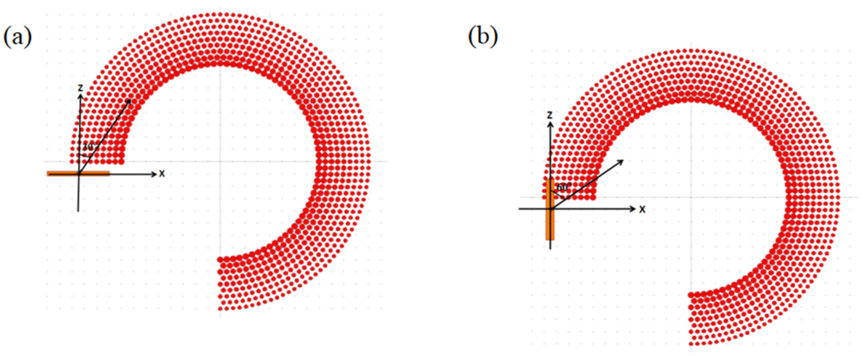
In 2006, John Pendry [17,34,35,36] and others respectively proposed the theory of an electromagnetic invisibility cloak. They found that, when the permittivity and permeability of the material satisfy certain relations, electromagnetic waves propagate along a given curve in the medium and are not reflected, thus mimicking a warped space-time. This means that electromagnetic waves can be freely manipulated by precise design. The use of artificially engineered microstructural meta-materials modifies the path of the wave so that it bypasses the object, rendering it invisible. According to this theory, cloaking materials are key to the development of cloaking technology, and the material parameters required are relatively demanding and even difficult to achieve for natural materials. In the past two decades, special coatings of matter, called materials, have been developed that allow electromagnetic radiation at certain wavelengths to pass freely around objects. This is different from the transmittance of light through matter. The structure of a meta-material directs light around an object, causing it to emit undisturbed in the direction it entered. In order to use an invisibility cloak to hide objects, one can design a specific light path to guide the light; that is, one can create a changeable electromagnetic field as needed, if the magnetic field structure is designed appropriately. If the bending of the incident light is controlled, the object in the magnetic field can be invisible at a specific wavelength. The large bend gradient waveguide structure designed above is the gradient radius of the dielectric nematic calculated from its analytical formula in the framework of MG theory; hence, the structure studied can also be considered as a class of graded dielectric meta-materials. The results already calculated above show that a dielectric rod with only one transfer (dB) material can be realized by changing the radius of the dielectric rod. This makes it possible to fabricate low-loss devices at optical frequencies. In the above simulation, the optical wave is incident at the cross section of the vertical waveguide. In the following, we modify the light incidence direction to observe the light propagation as Figure 15a in which the light incident is at an angle of 30 degrees between the vertical di-rection and the vertical direction and Figure 15b in which light is incident at an angle of 60 degrees from the vertical direction.
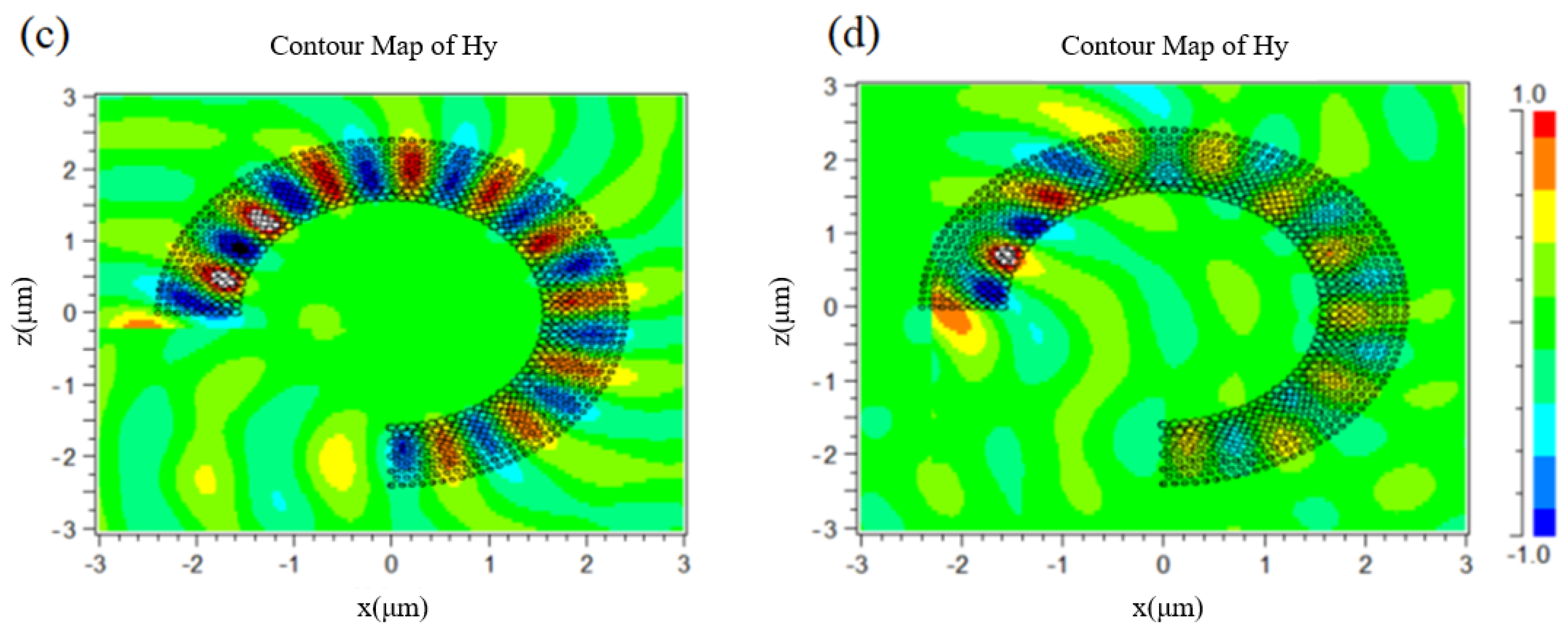
As can be seen from the graphical results, the light can still propagate along the structure and does not enter the interior of the structure when incident obliquely along the 30 degree deflection direction in Figure 15c. However, when the light is obliquely incident along the 60 degree deflection direction, the light has deviated from the control in Figure 15d. It can be seen that, at present, such structures can only realize the free control of light waves through some special directions. Designing ultra-structured materials that bend incident light from any angle and distance around an object and display the object’s background remains a great challenge.

6. Conclusions

In this paper, based on Maxwell–Garnett theory, three kinds of gradual large bending waveguides are designed by changing the constant parameter C. The three waveguides are analyzed in the following aspects: In the first, the transmission of light waves propagating in the medium is analyzed, and it is proved that the bending loss is minor and the degree of freedom is higher because of the high circular symmetry. In the second, considering the difficulty of the future production process, the robustness analysis is carried out to confirm its excellent fault tolerance. In the third, we explored its value in the use of optical integrated devices and as a material selection. It is proved that the gradual bending waveguide of Sunflower, as a connection device of a straight waveguide, can effectively avoid the loss caused by the mode mismatch problem. It shows its application value in integrated optical devices. The stealth effect of visible light as a meta-material is simulated by different incidence angles of visible light. At present, such a structure can only play a stealth effect on a specific range of incident direction of light (that is, to achieve free control of light waves); to achieve full-angle stealth is still a huge challenge.

Author Contributions

Conceptualization, W.L. and X.S.; methodology, W.L.; software, W.L.; validation, X.S.; formal analysis, X.S.; investigation, H.L.; resources, F.Z.; data curation, W.L.; writing—original draft preparation, W.L.; writing—review and editing, W.L.; supervision, H.L.; project administration, H.L.; funding acquisition, H.L. All authors have read and agreed to the published version of the manuscript.

Funding

This research was funded by [Research Foundation for Advanced Talents of North China University of Water Resources and Electric Power] grant number [201803021] And The APC was funded by [201803021].

Institutional Review Board Statement

Not applicable.

Informed Consent Statement

Not applicable.

Data Availability Statement

No new data were created or analyzed in this study. Data sharing is not applicable to this article.

Acknowledgments

Research Foundation for Advanced Talents of North China University of Water Resources and Electric Power (Project’s Number: 201803021). The Opening Foundation of Henan Key Laboratory of Laser and Opto-electric Information Technology, School of Information Engineering (Project’s Number: JG2021-RF01). Key projects of Henan Provincial Department of Education (Project’s Number: 192102210253).

Conflicts of Interest

The authors declare no conflict of interest.

References

  1. John, S. Strong localization of photons in certain disordered dielectric superlattices. Phys. Rev. Lett. 1987, 58, 2486–2488. [Google Scholar] [CrossRef] [Green Version]
  2. Yablonovitch, E. Inhibited spontaneous emission in solid-state physics and electronics. Phys. Rev. Lett. 1987, 58, 2059–2061. [Google Scholar] [CrossRef] [PubMed] [Green Version]
  3. Centeno, E.; Cassagne, D. Graded photonic crystals. Opt. Lett. 2005, 30, 2278–2280. [Google Scholar] [CrossRef] [PubMed]
  4. Centeno, E.; Cassagne, D.; Albert, J.-P. Mirage and superbending effect in two-dimensional graded photonic crystals. Phys. Rev. B 2006, 73, 235119. [Google Scholar] [CrossRef]
  5. Vasić, B.; Gajić, R. Self-focusing media using graded photonic crystals: Focusing, fourier transforming and imaging, directive emission, and directional cloaking. J. Appl. Phys. 2011, 110, 0531031–0531038. [Google Scholar] [CrossRef]
  6. Russell, P.S.J.; Birks, T.A. Hamiltonian optics of nonuniform photonic crystals. J. Light. Technol. 1999, 17, 1982. [Google Scholar] [CrossRef]
  7. Jiao, Y.; Fan, S.; Miller, D.A.B. Designing for beam propagation in periodic and nonperiodic photonic nanostructures: Extended Hamiltonian method. Phys. Rev. E 2004, 70, 036612. [Google Scholar] [CrossRef] [PubMed]
  8. Gao, F.; Qin, L.; Chen, Y.; Jia, P.; Chen, C.; Liang, L.; Chen, H.; Zhang, X.; Ning, Y. Research progress and application of curved waveguides. Chin. Opt. 2017, 10, 18. [Google Scholar]
  9. Mei, Z.L.; Cui, T.J. Experimental realization of a broadband bend structure using gradient index metamaterials. Opt. Express 2009, 17, 18354–18363. [Google Scholar] [CrossRef]
  10. Vasić, B.; Isić, G.; Gajić, R.; Hingerl, K. Coordinate transformation based design of confined metamaterial structures. Phys. Rev. B 2009, 79, 085103. [Google Scholar] [CrossRef] [Green Version]
  11. Vasić, B.; Isić, G.; Gajić, R.; Hingerl, K. Controlling electromagnetic fields with graded photonic crystals in metamaterial regime. Opt. Express 2010, 18, 20321–20333. [Google Scholar] [CrossRef]
  12. Scheuer, J.; Yariv, A. Circular photonic crystal resonators. Phys. Rev. E 2004, 70, 036603. [Google Scholar] [CrossRef] [PubMed]
  13. Chang, D.; Scheuer, J.; Yariv, A. Optimization of circular photonic crystal cavities-beyond coupled mode theory. Opt. Express 2005, 13, 9272–9279. [Google Scholar] [CrossRef] [Green Version]
  14. Li, D.; Pu, S.; Zhao, Y.; Li, Y.; Hao, Z.; Han, Z. Sensing properties of symmetrical side-polished photonic crystal fiber based on surface plasmon resonance. Opt.-Int. J. Light Electron Opt. 2020, 224, 165662. [Google Scholar] [CrossRef]
  15. Pu, S.; Bai, X.; Wang, L. Temperature dependence of photonic crystals based on thermoresponsive magnetic fluids. J. Magn. Magn. Mater. 2011, 323, 2866. [Google Scholar] [CrossRef]
  16. Kamau, S.; Hassan, S.; Alnasser, K.; Zhang, H.; Cui, J.; Lin, Y. Broadband Absorption in Patterned Metal/Weakly-Absorbing-Spacer/Metal with Graded Photonic Super-Crystal. Photonics 2021, 8, 114. [Google Scholar] [CrossRef]
  17. Pendry, J.B.; Schurig, D.; Smith, D.R. Controlling Electromagnetic Fields. Science 2006, 312, 1780–1782. [Google Scholar] [CrossRef] [Green Version]
  18. Li, Z.-W. Study on the Regulation of Electromagnetic Wave by Artificially Structured Metasurface and One-Dimensional Photonic Crystal. Ph.D. Thesis, Huazhong University of Science and Technology, Wuhan, China, 2016. [Google Scholar] [CrossRef]
  19. Savotchenko, S.E. Surface waves in a linearly graded-index and an intensity-dependent index layered structure. J. Opt. Soc. Am. A 2022, 39, 1210–1217. [Google Scholar] [CrossRef] [PubMed]
  20. Hassan, S.; Sale, O.; Lowell, D.; Hurley, N.; Lin, Y. Holographic Fabrication and Optical Property of Graded Photonic Super-Crystals with a Rectangular Unit Super-Cell. Photonics 2018, 5, 34. [Google Scholar] [CrossRef] [Green Version]
  21. Badri, S.H.; Gilarlue, M.M. Low-index contrast waveguide bend based on truncated Eaton lens implemented by graded photonic crystals. J. Opt. Soc. Am. B 2019, 36, 1288–1293. [Google Scholar] [CrossRef]
  22. Zhang, H.; Qian, L.; Wang, C.; Ji, C.-Y.; Liu, Y.; Chen, J.; Lu, C. Topological rainbow based on graded topological photonic crystals. Opt. Lett. 2021, 46, 1237–1240. [Google Scholar] [CrossRef] [PubMed]
  23. Xiao, S.; Qiu, M. High-Q microcavities realized in a circular photonic crystal slab. Photonics Nanostruct.-Fundam. Appl. 2005, 3, 134–138. [Google Scholar] [CrossRef]
  24. Xiao, S.; Qiu, M. Study of transmission properties for waveguide bends by use of a circular photonic crystal. Phys. Lett. A 2005, 340, 474–479. [Google Scholar] [CrossRef] [Green Version]
  25. Sun, X.H.; Wu, Y.L.; Liu, W.; Hao, Y.; Jiang, L.-D. Luneburg lens composed of sunflower-type graded photonic Crystals. Opt. Commun. 2014, 315, 367–373. [Google Scholar] [CrossRef]
  26. David, L.; Safaa, H.; Murthada, A.; Hurley, N.; Philipose, U.; Chen, B.; Lin, Y. Holographic fabrication of graded photonic super-crystals using an integrated spatial light modulator and reflective optical element laser projection system. Appl. Opt. 2017, 56, 9888. [Google Scholar]
  27. Hurley, N.; Kamau, S.; Alnasser, K.; Philipose, U.; Cui, J.; Lin, Y. Laser Diffraction Zones and Spots from Three-Dimensional Graded Photonic Super-Crystals and Moiré Photonic Crystals. Photonics 2022, 9, 395. [Google Scholar] [CrossRef]
  28. Qi, Y.; Liu, K.; Wang, S.; Chen, D.; Sun, X. Focusing characteristics of graded photonic crystal waveguide lens based on interference lithography. Opt. Eng. 2021, 60, 077102. [Google Scholar] [CrossRef]
  29. Taylor, H.F. Power loss at directional change in dielectric waveguides. Appl. Opt. 1974, 13, 642–647. [Google Scholar] [CrossRef] [PubMed]
  30. Neumann, E.G. Curved Dielectric Optical Waveguide with Reduced Transition Losses. Microw. Antennas Propag. 1982, 129, 278–280. [Google Scholar] [CrossRef]
  31. Smit, M.K.; Pennings, E.C.M.; Blok, H. A normalized approach to the design of low-loss optical wave-guide bends. J. Light. Technol. 1993, 11, 1737–1742. [Google Scholar] [CrossRef]
  32. Fan, G.; Sang, W.; Liu, X.; Zhen, Z. Silicon waveguide racetrack resonators with 1.5 μm radius using junction offsets. Microw. Opt. Technol. Lett. 2012, 54, 1470–1471. [Google Scholar] [CrossRef]
  33. Ladouceur, F.; Labeye, P. A new general-approach to optical wave-guide path design. J. Light. Technol. 1995, 13, 481–492. [Google Scholar] [CrossRef]
  34. Schurig, D.; Mock, J.J.; Justice, B.J.; Cummer, S.A.; Pendry, J.B.; Starr, A.F.; Smith, D.R. Metamaterial Electromagnetic Cloak at Microwave Frequencies. Science 2006, 314, 977–980. [Google Scholar] [CrossRef] [Green Version]
  35. Cai, W.; Chettiar, U.K.; Kildishev, A.V.; Shalaev, V.M. Optical cloaking with metamaterials. Nat. Photonics 2007, 1, 224–227. [Google Scholar] [CrossRef] [Green Version]
  36. Liu, R.; Ji, C.; Mock, J.J.; Chin, J.Y.; Cui, T.J.; Smith, D.R. Broadband Ground-Plane Cloak. Science 2009, 323, 366–369. [Google Scholar] [CrossRef]
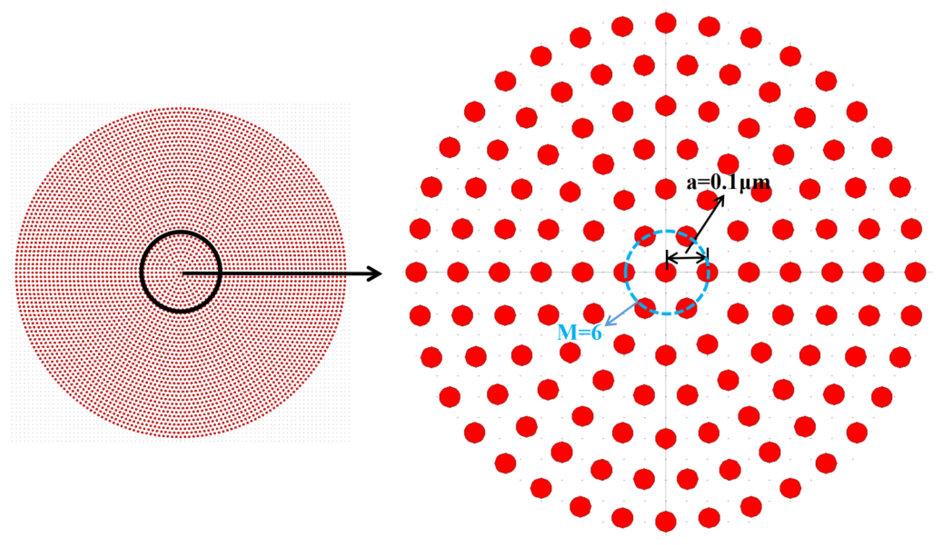
Figure 1. Sunflower structure schematic diagram.
Photonics 10 00781 g001
Figure 2. Transmission spectra of Sunflower PCs with different filling factors.
Photonics 10 00781 g002
Figure 3. Schematic diagram of the gradient waveguide structure.
Photonics 10 00781 g003
Figure 4. Sunflower gradient waveguide structure model.
Photonics 10 00781 g004
Figure 5. Electric field distribution of Sunflower waveguide at three communication wavelengths: (a) 0.85 µm, (b) 1.31 µm and (c) 1.55 µm.
Photonics 10 00781 g005
Figure 6. Transmission coefficients when refractive index is 3.12~2.38.
Photonics 10 00781 g006
Figure 7. Electric field distribution of Sunflower waveguide with refractive index of 3.12~2.38 at three communication wavelengths: (a) 0.85 µm, (b) 1.31 µm, and (c) 1.55 µm.
Photonics 10 00781 g007
Figure 8. When C = 3, electric field distribution of Sunflower waveguide with refractive index of 3~2 at three communication wavelengths: (a) 0.85 µm, (b) 1.31 µm, and (c) 1.55 µm.
Photonics 10 00781 g008
Figure 9. When C = 7, electric field distribution of Sunflower waveguides with refractive indexes of 3.18~2.69 at three communication wavelengths: (a) 0.85 µm, (b) 1.31 µm, and (c) 1.55 µm.
Photonics 10 00781 g009
Figure 10. Transmission coefficients when: (a) C = 3, (b) C = 7.
Photonics 10 00781 g010
Figure 11. Imperfect gradient waveguide: (a) model with two adjacent layers of rods keep the diameter unchanged, (b) model with points defect.
Photonics 10 00781 g011
Figure 12. Electric field distribution of Sunflower waveguide with for Figure 11a at three communication wavelengths: (a) 0.85 µm, (b) 1.31 µm, and (c) 1.55 µm.
Photonics 10 00781 g012
Figure 13. Electric field distribution of Sunflower waveguide with for Figure 11b at three communication wavelengths: (a) 0.85 µm, (b) 1.31 µm, and (c) 1.55 µm.
Photonics 10 00781 g013
Figure 14. (a) Amplitude distributions, wave-front, and time mean Poynting vectors of the fundamental modes on the sections of straight and curved dielectric waveguides [30]. (b) Curved waveguide and linear waveguide sections with offset [31]. (c) The incident light enters the model vertically from the center of the incident plane. (d) The incident light enters the model vertically at a deviation of 0.3 µm from the center of the incident plane to the left (e). Electric field distribution of Sunflower waveguide with for Figure 14c. (f) Electric field distribution of Sunflower waveguide with for Figure 14d.
Photonics 10 00781 g014
Figure 15. (a) Schematic diagram of the model in which the light incident is at an angle of 30 degrees between the vertical direction and the vertical direction. (b) Schematic diagram of the model in which light is incident at an angle of 60 degrees from the vertical direction. (c) The distribution of its light field. (d) The distribution of its light field.
Photonics 10 00781 g015aPhotonics 10 00781 g015b
Table 1. Distribution parameters of media column.
ρ (µm)nr (µm)
1.63.1250.047963
1.72.9411764710.047943
1.82.7777777780.04492
1.92.6315789470.042192
22.50.039716
2.12.3809523810.037453
2.22.2727272730.035376
2.32.1739130430.033458
2.42.0833333330.031679
2.520.030022
2.61.9230769230.028472
2.71.8518518520.027016
2.81.7857142860.025644
2.91.7241379310.024345
31.6666666670.023111
3.11.6129032260.021935
3.21.56250.02081
3.31.5151515150.01973
3.41.4705882350.01869
3.51.4285714290.017684
3.61.3888888890.016707
3.71.3513513510.015755
3.81.3557894740.014832
3.91.2820512820.013906
41.250.013
Table 2. Distribution parameters of media column at C = 3.
ρ (µm)nr (µm)
130.04582
1.12.7270.0411
1.22.50.03711
1.32.3080.03369
1.42.1430.0307
1.520.02805
Table 3. Distribution parameters of media column at C = 7.
ρ (µm)nr (µm)
2.23.1820.04893
2.33.0430.04656
2.42.9170.04438
2.52.80.04236
2.62.6920.04049
Disclaimer/Publisher’s Note: The statements, opinions and data contained in all publications are solely those of the individual author(s) and contributor(s) and not of MDPI and/or the editor(s). MDPI and/or the editor(s) disclaim responsibility for any injury to people or property resulting from any ideas, methods, instructions or products referred to in the content.