Article

An Ultrabroadband and Cost-Effective Edge Coupler for Efficient Thin Film Lithium Niobate Photonics

State Key Laboratory of Optoelectronic Materials and Technologies, School of Physics, Sun Yat-sen University, Guangzhou 510275, China
*
Author to whom correspondence should be addressed.
Photonics 2023, 10(7), 760; https://doi.org/10.3390/photonics10070760
Submission received: 26 May 2023 / Revised: 23 June 2023 / Accepted: 28 June 2023 / Published: 1 July 2023

Abstract

:
Due to attractive material properties, thin film lithium niobate (TFLN) has emerged as a promising platform for advanced photonic functions such as high-speed electro-optical modulation, nonlinear frequency conversion, and frequency comb generation. The inevitable problems for the practical above-mentioned applications are the large coupling loss between the fiber and the TFLN waveguide and difficulty in achieving broadband coupling, especially covering the near-visible to near-infrared. Here, we theoretically propose a low-loss and ultrabroadband edge coupler with a six-layer structure. For transverse electric (TE) polarized light, the proposed coupler can achieve 0.62 dB, 0.38 dB, and 0.47 dB per facet at three common communication bands, 845 nm, 1310 nm, and 1550 nm, respectively. From 1200 nm to 2000 nm, the coupling loss is less than 1 dB/facet. Moreover, in the near-visible to near-infrared region ranging from 845 nm to 2000 nm, the coupling loss is lower than 2 dB/facet. The proposed coupler can avoid expensive electron beam lithography. Instead, it can be fabricated by i-line ultraviolet lithography, which is cost-effective and adaptable to wafer-scale fabrication. Also, simulated fabrication tolerances demonstrate the strong robustness of the proposed coupler. Our results pave a way towards practical TFLN photonic devices connected with optical fibers.

1. Introduction

Lithium niobate (LN) is considered a promising candidate for integrated photonics and has been applied in photonics areas for a long time. Compared with other material systems (silicon [1,2], silicon nitride [3,4], gallium arsenide [5], etc.), LN has many excellent properties, such as wide transparent windows (400–5000 nm), large second-order nonlinearity (d33 = 27 pm/V), and outstanding electro-optic properties (r33 = 30.9 pm/V) [6,7,8,9,10]. Conventional LN devices are typically implemented by diffused technologies such as reverse-proton exchange [11,12,13]. These diffused technologies can only provide a small refractive index contrast (∆n ~ 0.02), resulting in weak confinement, a large mode field diameter, and a large bending radius, which is not conducive to integration. Fortunately, the emergence of thin film lithium niobate (TFLN, typically hundreds of nanometers of lithium niobate on top of a 2 µm or 4.7 µm thick buried silica layer supported by a silicon substrate) and progress in etching LN have provided an unlimited possibility for integrated LN photonics. Due to a high refractive index contrast (∆n ~ 0.7), devices based on TFLN are able to achieve tighter confinement and stronger light–matter interaction, with a mode field diameter (MFD) of typically only 1 µm or smaller. Recently, a great number of outstanding devices based on TFLN have been reported, such as upconversion single-photon detectors [14], frequency converters [15,16,17,18,19,20,21,22,23], electro-optic modulators [24,25,26], frequency combs [27], etc.
However, there are many challenges and difficulties in the further development and practical application of devices based on TFLN. The most obvious one is the large coupling loss between the optical fiber and the submicrometer TFLN waveguide due to their large mode sizes’ mismatch. The high coupling loss compromises the optical power delivered into the TFLN waveguide, thus restricting the overall performances of the above photonic devices. Another is the difficulty in achieving broadband coupling, especially covering the near-visible to the near-infrared. For example, for applications such as frequency conversion interfaces, upconversion single-photon detectors, and corresponding photonic systems, which typically involve two or more photons with significant frequency difference [28,29,30], the coupling bandwidth is crucial and dramatically affects their performances. Couplers between the optical fiber and the LN chip are usually employed to cope with the coupling issue mentioned above. They can be simply divided into two categories: vertical couplers and edge couplers, according to the coupling direction. Vertical couplers, mostly grating couplers [31,32,33,34,35,36,37,38], intrinsically suffer from limited efficiency, limited bandwidth, and polarization sensitivity due to their operational principle. As for edge couplers [39,40,41,42,43,44,45,46,47], taper waveguide structures are usually used in the design and preferred in practical applications, especially in areas with high requirements for both coupling efficiency and bandwidth, such as upconversion single-photon detectors.
Recently, various edge couplers based on TFLN have been reported. After shrinking the tapered tip to match the lensed fiber, a bilayer taper shows a coupling loss of 1.7 dB/facet [39]. To further improve the coupling efficiency, a coupler consisting of a bilayer taper and a SiON cladding waveguide is proposed that displayed a coupling loss lower than 1 dB/facet in the wavelength range of 1527 nm to 1630 nm [41]. In order to extend the coupling bandwidth to the near-visible band, a coupler comprising a tri-layer taper and a silica cladding waveguide is reported that exhibited a coupling loss of 1 dB/facet and 3 dB/facet at 1550 nm and 775 nm, respectively [44]. Although the performance of the above coupler is outstanding, the fabrication of such a coupler requires high-precision electron-beam lithography, which is expensive and detrimental to wafer-scale fabrication. Predictably, with the development of LN photonics, it is important to integrate all kinds of LN functional components on a single wafer. Therefore, to take full advantage of TFLN, a coupler that can be manufactured at wafer-scale using ultraviolet lithography and is low loss, ultrabroadband, and cost-effective is highly desired.
In this paper, we theoretically propose a low-loss, ultrabroadband, and cost-effective edge coupler, with a six-layer structure, that can be fabricated by i-line ultraviolet lithography and is able to avoid expensive high-precision electron beam lithography. For transverse electric (TE) polarized light, the proposed coupler can achieve 0.62 dB, 0.38 dB, and 0.47 dB per facet at three common communication bands, 845 nm, 1310 nm, and 1550 nm, respectively. From 1200 nm to 2000 nm, the coupling loss is less than 1 dB/facet. Moreover, the proposed coupler achieves a coupling loss of less than 2 dB/facet in the near-visible to the near-infrared region ranging from 845 nm to 2000 nm. The influences of misalignment, etching depth deviation, and sidewall angle deviation are also simulated, showing a large fabrication tolerance. Our approach opens a door for future practical integrated LN photonic devices and corresponding applications.

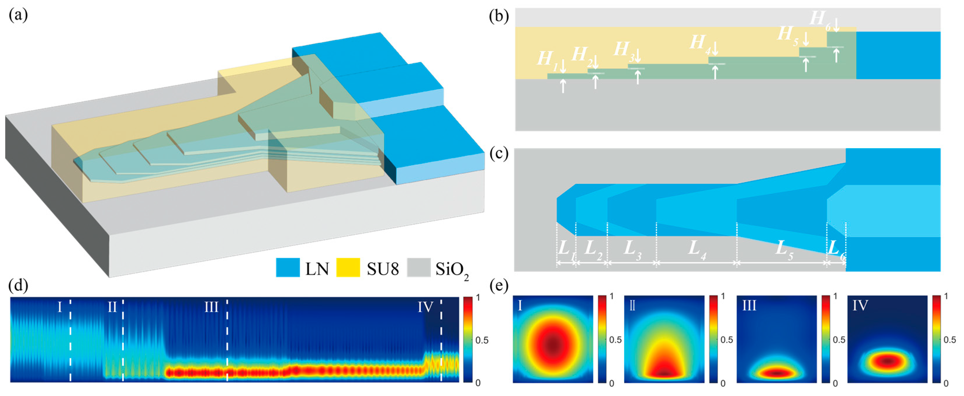
2. Principle of the Multilayer Coupler

The schematic structure of the coupler is shown in Figure 1a–c. The proposed coupler, composed of a multilayer spot size converter (SSC) and an SU8 cladding waveguide (CWG), is based on x-cut TFLN. When light is coupled from the fiber to the chip, both the SSC and the CWG play an important role. The CWG not only improves the mode overlap between fiber and chip but also reduces the possibility of light leakage to the cladding silica or substrate. The multilayer SSC, whose light confinement gradually increases with the increase of the number of layers and the coupling length, can adiabatically couple the light from the CWG into the waveguide. As shown in Figure 1d,e, we selected 1064 nm (TE mode) for the analysis and showed the mode evolution along the propagation direction and the mode field distribution at different cross-sections. It is apparent that after the light is incident from the fiber to the coupler, the light is progressively coupled into the waveguide along the propagation direction. Detailed design parameters of the CWG and SSC are described in Part 3.
For a given fiber, an SSC that is suitable for short waves often fails to form effective confinement at long wavelengths. Conversely, if an SSC is properly used to couple long waves, its tapered tip will cause too tight a confinement for short waves and hence a large mode mismatch, which will lead to a decreased coupling efficiency at short wavelengths. Thus, for broadband coupling, because the demand for the SSC is different for different wavelengths when the coupling efficiency and bandwidth are both considered, we need to meet the coupling requirements for short waves first and then achieve tight confinement and efficient coupling for long waves through the adjustment of the height of the SSC.
Also, on the point of fabrication, we would like to reduce the fabrication difficulty and cost by using i-line ultraviolet lithography, which will inevitably make the horizontal width of the SSC larger. However, in the practical fabrication process, the longitudinal height of the SSC can be controlled by the etching time far more easily than with the small-size electron beam lithography in the horizontal direction. Therefore, we increase the number of layers in order to adjust the confinement capacity of the SSC.
To better illustrate the principles, we use the finite-difference eigenmode (FDE) solver (Mode Solutions, Anays/Lumerical) to calculate the modal distribution and mode area of the SSC at different heights, as shown in Figure 2. In the designed coupling bandwidth, we select 845 nm, 1064 nm, 1310 nm, 1550 nm, 1950 nm, and 2000 nm TE fundamental modes as the reference light (RL) for the analysis, as they are commonly used wavelengths in fiber-optic communication and lithium niobate nonlinear optics. In the structural design, we fixed the sidewall angle and minimum width of the SSC to the commonly used 60° and the common minimum feature size of 1 μm for i-line ultraviolet lithography, respectively. Figure 2a–f shows the mode field distribution of the RL for the SSC with the same CWG, the same sidewall angle, the same 1 μm width, and the same 75 nm height. It is obvious that there is a significant difference in the confinement of the SSC at different wavelengths, which proves the above conclusion that the demands for the SSC at different wavelengths are different.
From Figure 2g, we can find that when the width is fixed (1 μm in this case), the modal area at different wavelengths undergoes a rapid drop at different heights and then gradually becomes a tightly confined steady state. Therefore, in the stage of rapid change of the modal area, the height change of the SSC should be as small as possible to reduce the coupling loss between adjacent layers. Ideally, the coupling loss between adjacent layers can be reduced to a negligible level when the number of layers is sufficient or when a three-dimensional structure with continuously varying height and width is formed [48], thus achieving a remarkably high coupling efficiency. Nevertheless, both of these scenarios undoubtedly create difficulties for practical fabrication. Hence, there is a tradeoff between the number of layers and the coupling efficiency, which is also a tradeoff between the simplest fabrication and the best performance. In the design, we need to balance the two and determine the proper parameters, which will be discussed in detail in Part 3.

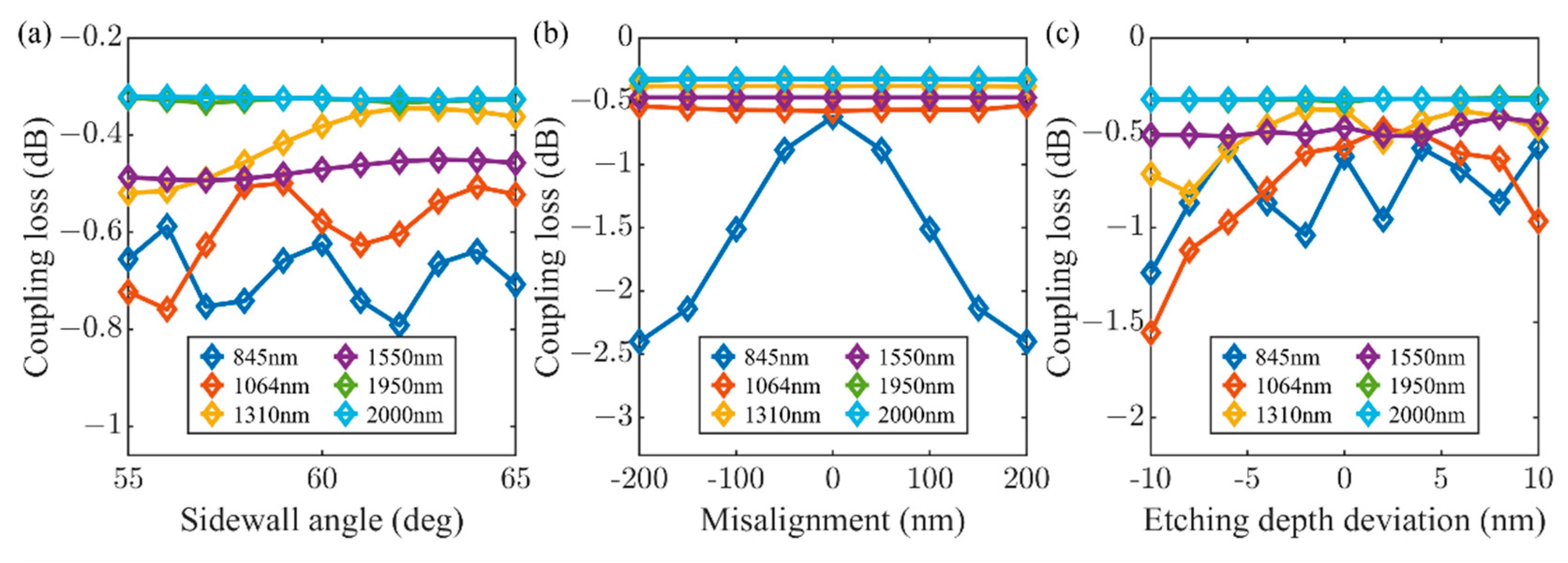
3. Simulation and Optimization

As shown in Figure 2, when the height of the SSC reaches 600 nm, all the light in the simulation range has reached a stable state. Therefore, we determine the platform for designing the coupler as an x-cut TFLN with 600 nm LN and 2 µm silica on the silicon substrate. In the x-cut TFLN, TE polarized light is used in most studies because of its capability to use the largest nonlinear coefficients and electro-optic coefficients, although transverse magnetic (TM) polarized light is sometimes used. Therefore, for the simplicity of expression, in the following discussion, we determine and optimize each parameter of the coupler using the TE fundamental mode and show the coupling performance of the TE and TM fundamental modes at the end of this section. During the simulation and optimization, the FDE solver and Eigenmode Expansion (EME) solver (Mode Solutions, Anays/Lumerical) are used as analytical tools. In the simulation setup, we use a lensed fiber with an MFD of 2 µm that has been widely applied experimentally.
Firstly, we determine the parameters of the CWG. To ensure efficient coupling of TE and TM polarized light at the same time, the cross-sectional shape of the CWG is chosen to be square, and its schematic diagram is shown in Figure 3a. We determine the size of the CWG by calculating the mode overlap between the lensed fiber and the CWG with different sizes. The overlap can be expressed as [43]:
O v e r l a p = ( E s × H c * · d S ) · ( E c × H f * · d S ) ( E f × H f * · d S ) · R e [ ( E c × H c * · d S ) ]
where Ef, Hf, Ec, and Hc represent the normalized electric (E) and magnetic (H) fields of the mode in the fiber (subscript f) and the CWG (subscript c), respectively. The calculation results for TE and TM polarized light are shown in Figure 3b and Figure 3c, respectively. Thanks to the isotropic of SU8 and the square structure of the CWG, Figure 3b,c is almost identical, which means that the CWG is polarization insensitive. Therefore, we set the width and height of the CWG as 1.8 μm, where the overlap of all RL is larger than 94%.
Secondly, after setting the dimensions of the CWG, we analyze and determine the height and length of each layer of the SSC. For the height of each layer of the SSC, the impact is mainly reflected in the coupling loss of light from the CWG to the first tapered structure and the coupling loss from the sudden change in height between adjacent layers. It is worth noting that, as discussed in the previous section, there is a clear tradeoff between the number of layers and the coupling efficiency. Fewer layers mean a larger height variation between layers, larger interlayer coupling loss, and ultimately larger coupling loss. Conversely, more layers lead to a higher coupling efficiency but also higher fabrication difficulty and cost. To solve this problem, we need a moderate group of parameters.
For this purpose, we first calculate and show the moderate parameters chosen in this paper. Then, different parameters are adjusted, targeting the best efficiency and the simplest process. Subsequently, the calculation results are compared. In this simulation, we assume that the length of each layer is sufficiently long and calculate the coupling efficiency of each group by the FDE and EME solvers. We calculate the coupling loss from the CWG to the first tapered structure and the coupling loss between each tapered structure, as shown in Figure 4. From Figure 4, we can obviously see that the larger the interlayer height variation is, the larger the coupling loss will be. At the same time, different wavelengths will experience a sudden increase in coupling loss at different heights. This result is consistent with the case of the modal area illustrated in Part 2. They are manifested as an abrupt change in coupling loss and the modal area, respectively. As a result, we need to set up enough layers in the rapid change stage to improve coupling efficiency according to the practical requirements. In most optical communications, 1 dB/facet is usually sufficient. Moreover, most of the existing research results are in the interval of 0.5~3 dB per facet. Therefore, we set the heights of the six tapered structures in the SSC as 45 nm, 30 nm, 35 nm, 60 nm, 130 nm, and 300 nm, respectively, as shown by the dashed lines in Figure 4 and Group A in Table 1.
Further, for a better demonstration of this balanced problem and to emphasize the generality of Group A, we choose two additional groups of parameters, denoted as Group B and Group C, under the same condition of a fixed LN thickness of 600 nm. They are composed of five- and seven-layer tapered structures, respectively, and the specific layer heights are shown in Table 1. As shown in Figure 5, we can find that all groups exhibit efficient coupling beyond 1220 nm. However, as the wavelength decreases, the difference between the groups becomes more and more obvious. When the number of layers is reduced to five, i.e., Group B, the coupling efficiency is relatively small in the range of 890 nm to 1200 nm. Also, there is a region that cannot be coupled effectively, such as the region smaller than 870 nm, which is detrimental to achieve broadband coupling. When the number of layers is increased to seven, i.e., Group C, the coupling efficiency is not significantly improved compared to Group A and is even reduced in some regions. As a result, the number of layers of SSC is set as six. Of course, if the actual requirements or goals change, we can adjust the number of layers to accommodate the change appropriately. For example, when we only need communication bands, such as the C-band, to keep low coupling loss, we can reduce the number of layers to five or four or even less, to three. Group B in this paper is a similar attempt.
For the coupling length of each layer of the SSC, it works to keep the mode field stable within each layer. The mode field needs some distance to complete the change and become stable. Therefore, with the selection of Group A, we use the EME solver to optimize and determine the coupling length of each layer in order to facilitate the goal of miniaturization and integration. The specific calculation method is to set the coupling length of each layer to be long enough and then scan the length of one of them successively to obtain the relationship between coupling length and coupling loss. As shown in Figure 6, we calculate and analyze all RL, and we can find that the trends of the curves are similar. As the coupling length increases, the coupling efficiency gradually increases from a large fluctuation at the beginning to a stable level. In accordance with the target of integration and low-loss and broadband traits, we set the coupling length of each layer as L1 = 100 μm, L2 = 200 μm, L3 = 200 μm, L4 = 400 μm, L5 = 450 μm, and L6 = 100 μm, respectively, as shown by the red star in Figure 6 and Group I of Table 2.
It is worth noting that the coupling length here is not the value to obtain the highest coupling efficiency but a compromise value after comprehensive consideration. If further efficiency improvements or smaller devices are desired, we can extend or shorten the length. As shown in Figure 7, we additionally select two groups of parameters, denoted as Group II and III. Then, we calculate their coupling performance and compare them with Group I. The specific lengths of Group II and III are shown in Table 2. From Figure 7, we can find that although Group III with a longer length can lead to coupling efficiency improvement, the improvement is very small, and the overall performance is very close to that of Group I. Therefore, the advantage of longer lengths is not considerable or cost-effective. For the shorter length, Group II, its coupling efficiency has a significant decrease and fluctuation compared to that of the other two groups, which is not in line with our target. However, if the target loss is 3 dB, Group II or even a shorter coupling length would be acceptable.
In short, for the height and length, we choose Group A and Group I, respectively. The performances of this proposed coupler are shown in Figure 8. It shows that TE polarized light can achieve a coupling loss of less than 2 dB/facet in the wavelength range from 845 nm to 2000 nm. Specifically, the coupling loss of 0.62 dB, 0.38 dB, and 0.47 dB per facet can be achieved in the three common communication bands at 845 nm, 1310 nm, and 1550 nm. Moreover, it shows an 800 nm wide coupling window in the 1200–2000 nm range with a 1 dB coupling loss. For TM polarized light, the coupling efficiency is decreased compared to that of TE polarized light, especially in the region of shorter wavelengths. This decrease is because the present parameters are mainly designed for TE polarized light, and the shorter wavelengths are more sensitive to the structure’s geometry. There may be a greater scattering loss for TM polarized light in the longitudinal direction. This problem can be solved by further optimization of the structure. Although the coupling performance of TM polarized light is not as good as that of TE polarized light, it still has high coupling performance in the working range, such as the coupling loss of 0.77 dB and 0.38 dB per facet at 1310 nm and 1550 nm, respectively. In addition, we compare the proposed coupler with other reported edge couplers based on TFLN in Table 3. We can observe that the proposed coupler is comparable to the state-of-the-art coupler in efficiency and has the advantage of large coupling bandwidth and wafer-scale fabrication.
Finally, we analyze the fabrication tolerance of this proposed coupler. Since the proposed coupler has a multilayer structure, multiple alignment exposures and etchings are required for the practical fabrication, which may introduce misalignment deviation and etching depth deviation. In addition, the sidewall angle of the SSC and waveguide may also deviate. Thus, we simulate the coupling loss for all RL with ±5° sidewall angle deviation, ±200 nm alignment deviation, and ±10 nm etching depth deviation, as shown in Figure 9. We can find that the deviation of the sidewall angle has a small effect on the proposed edge coupler, and the additional coupling loss caused by ±5° deviation is no more than 0.2 dB. The impact of misalignment and etching depth on the coupler is mainly found at short wavelengths, such as 845 nm and 1064 nm. This tendency is because short wavelengths are more sensitive to the coupler geometry than long wavelengths. This problem can be solved by further optimization of the coupler structure, such as adjusting the width and height of the SSC. At other wavelengths, the impact of the misalignment on the coupling loss is no more than 0.4 dB. Therefore, the proposed coupler has high fabrication robustness.

4. Conclusions

In this paper, we theoretically propose an edge coupler consisting of a six-layer SSC and an SU8 CWG, with strong robustness. Due to the multilayer design and optimization, the proposed coupler is low-loss and ultrabroadband. For TE polarized light, an ultrawide coupling window from 845 nm to 2000 nm with a coupling loss lower than 2 dB/facet can be achieved. Specifically, the coupler can achieve a low coupling loss of 0.62 dB, 0.38 dB, and 0.47 dB per facet at three common communication bands, 845 nm, 1310 nm, and 1550 nm, respectively. Compared to current LN edge couplers, the proposed coupler can be fabricated by an i-line ultraviolet lithography technique, which is cost-effective and adaptable to wafer-scale fabrication. In the future, the proposed coupler can be further simplified by optimizing the SSC profile, such as using parabolic and exponential shapes or introducing subwavelength gratings.
In short, our proposed coupler provides a novel solution for TFLN photonic devices connecting with optical fibers and shows great promise for practical applications based on TFLN, such as frequency converters that involve photons with a significant frequency difference and wafer-scale multifunctional integrated LN devices.

Author Contributions

Conceptualization, F.M.; methodology, F.M. and H.C.; investigation, software, H.C.; writing—original draft preparation, H.C.; writing—review and editing, F.M. and J.D.; supervision, F.M. and J.D.; project administration, F.M. and J.D.; funding acquisition, F.M., K.C., and J.D. All authors have read and agreed to the published version of the manuscript.

Funding

National Natural Science Foundation of China (62105374); Basic and Applied Basic Research Foundation of Guangdong Province (2023A1515012723, 2023B1515040023, 2020A1515110192); Guangzhou Municipal Science and Technology Bureau (202102021157); Fundamental Research Funds for the Central Universities, Sun Yat-sen University (23qnpy59).

Institutional Review Board Statement

Not applicable.

Informed Consent Statement

Not applicable.

Data Availability Statement

Not applicable.

Conflicts of Interest

The authors declare no conflict of interest.

References

  1. Jalali, B.; Fathpour, S. Silicon Photonics. J. Light. Technol. 2006, 24, 4600–4615. [Google Scholar] [CrossRef]
  2. Leuthold, J.; Koos, C.; Freude, W. Nonlinear silicon photonics. Nat. Photonics 2010, 4, 535–544. [Google Scholar] [CrossRef]
  3. Xiang, C.; Jin, W.; Bowers, J.E. Silicon nitride passive and active photonic integrated circuits: Trends and prospects. Photonics Res. 2022, 10, A82–A96. [Google Scholar] [CrossRef]
  4. Riley, F.L. Silicon Nitride and Related Materials. J. Am. Ceram. Soc. 2000, 83, 245–265. [Google Scholar] [CrossRef]
  5. Adachi, S. GaAs, AlAs, and AlxGa1−xAs: Material parameters for use in research and device applications. J. Appl. Phys. 1985, 58, R1–R29. [Google Scholar] [CrossRef]
  6. Weis, R.; Gaylord, T. Lithium niobate: Summary of physical properties and crystal structure. Appl. Phys. A 1985, 37, 191–203. [Google Scholar] [CrossRef]
  7. Boes, A.; Corcoran, B.; Chang, L.; Bowers, J.; Mitchell, A. Status and potential of lithium niobate on insulator (LNOI) for photonic integrated circuits. Laser Photonics Rev. 2018, 12, 1700256. [Google Scholar] [CrossRef]
  8. Vazimali, M.G.; Fathpour, S. Applications of thin-film lithium niobate in nonlinear integrated photonics. Adv. Photonics 2022, 4, 034001. [Google Scholar] [CrossRef]
  9. Lin, J.; Bo, F.; Cheng, Y.; Xu, J. Advances in on-chip photonic devices based on lithium niobate on insulator. Photonics Res. 2020, 8, 1910–1936. [Google Scholar] [CrossRef]
  10. Boes, A.; Chang, L.; Langrock, C.; Yu, M.; Zhang, M.; Lin, Q.; Lončar, M.; Fejer, M.; Bowers, J.; Mitchell, A. Lithium niobate photonics: Unlocking the electromagnetic spectrum. Science 2023, 379, eabj4396. [Google Scholar] [CrossRef]
  11. Parameswaran, K.R.; Route, R.K.; Kurz, J.R.; Roussev, R.V.; Fejer, M.M.; Fujimura, M. Highly efficient second-harmonic generation in buried waveguides formed by annealed and reverse proton exchange in periodically poled lithium niobate. Opt. Lett. 2002, 27, 179–181. [Google Scholar] [CrossRef] [Green Version]
  12. Roussev, R.V.; Langrock, C.; Kurz, J.R.; Fejer, M.M. Periodically poled lithium niobate waveguide sum-frequency generator for efficient single-photon detection at communication wavelengths. Opt. Lett. 2004, 29, 1518–1520. [Google Scholar] [CrossRef] [PubMed]
  13. Suntsov, S.; Rüter, C.E.; Brüske, D.; Kip, D. Watt-level 775 nm SHG with 70% conversion efficiency and 97% pump depletion in annealed/reverse proton exchanged diced PPLN ridge waveguides. Opt. Express 2021, 29, 11386–11393. [Google Scholar] [CrossRef] [PubMed]
  14. Wang, X.; Jiao, X.; Wang, B.; Liu, Y.; Xie, X.-P.; Zheng, M.-Y.; Zhang, Q.; Pan, J.-W. Quantum frequency conversion and single-photon detection with lithium niobate nanophotonic chips. NPJ Quantum Inf. 2023, 9, 38. [Google Scholar] [CrossRef]
  15. Wang, C.; Langrock, C.; Marandi, A.; Jankowski, M.; Zhang, M.; Desiatov, B.; Fejer, M.M.; Lončar, M. Ultrahigh-efficiency wavelength conversion in nanophotonic periodically poled lithium niobate waveguides. Optica 2018, 5, 1438–1441. [Google Scholar] [CrossRef] [Green Version]
  16. Chen, J.-Y.; Ma, Z.-H.; Sua, Y.M.; Li, Z.; Tang, C.; Huang, Y.-P. Ultra-efficient frequency conversion in quasi-phase-matched lithium niobate microrings. Optica 2019, 6, 1244–1245. [Google Scholar] [CrossRef]
  17. Lu, J.; Surya, J.B.; Liu, X.; Bruch, A.W.; Gong, Z.; Xu, Y.; Tang, H.X. Periodically poled thin-film lithium niobate microring resonators with a second-harmonic generation efficiency of 250,000%/W. Optica 2019, 6, 1455–1460. [Google Scholar] [CrossRef] [Green Version]
  18. Zhao, J.; Rüsing, M.; Javid, U.A.; Ling, J.; Li, M.; Lin, Q.; Mookherjea, S. Shallow-etched thin-film lithium niobate waveguides for highly-efficient second-harmonic generation. Opt. Express 2020, 28, 19669–19682. [Google Scholar] [CrossRef]
  19. Niu, Y.; Lin, C.; Liu, X.; Chen, Y.; Hu, X.; Zhang, Y.; Cai, X.; Gong, Y.-X.; Xie, Z.; Zhu, S. Optimizing the efficiency of a periodically poled LNOI waveguide using in situ monitoring of the ferroelectric domains. Appl. Phys. Lett. 2020, 116, 101104. [Google Scholar] [CrossRef]
  20. Park, T.; Stokowski, H.S.; Ansari, V.; McKenna, T.P.; Hwang, A.Y.; Fejer, M.; Safavi-Naeini, A.H. High-efficiency second harmonic generation of blue light on thin-film lithium niobate. Opt. Lett. 2022, 47, 2706–2709. [Google Scholar] [CrossRef]
  21. Wu, X.; Zhang, L.; Hao, Z.; Zhang, R.; Ma, R.; Bo, F.; Zhang, G.; Xu, J. Broadband second-harmonic generation in step-chirped periodically poled lithium niobate waveguides. Opt. Lett. 2022, 47, 1574–1577. [Google Scholar] [CrossRef] [PubMed]
  22. Lin, J.; Yao, N.; Hao, Z.; Zhang, J.; Mao, W.; Wang, M.; Chu, W.; Wu, R.; Fang, Z.; Qiao, L. Broadband quasi-phase-matched harmonic generation in an on-chip monocrystalline lithium niobate microdisk resonator. Phys. Rev. Lett. 2019, 122, 173903. [Google Scholar] [CrossRef] [PubMed]
  23. Huang, Z.; Luo, K.; Feng, Z.; Zhang, Z.; Li, Y.; Qiu, W.; Guan, H.; Xu, Y.; Li, X.; Lu, H. Resonant enhancement of second harmonic generation in etchless thin film lithium niobate heteronanostructure. Sci. China Phys. Mech. Astron. 2022, 65, 104211. [Google Scholar] [CrossRef]
  24. Wang, C.; Zhang, M.; Stern, B.; Lipson, M.; Lončar, M. Nanophotonic lithium niobate electro-optic modulators. Opt. Express 2018, 26, 1547–1555. [Google Scholar] [CrossRef] [Green Version]
  25. Wang, C.; Zhang, M.; Chen, X.; Bertrand, M.; Shams-Ansari, A.; Chandrasekhar, S.; Winzer, P.; Lončar, M. Integrated lithium niobate electro-optic modulators operating at CMOS-compatible voltages. Nature 2018, 562, 101–104. [Google Scholar] [CrossRef]
  26. He, M.; Xu, M.; Ren, Y.; Jian, J.; Ruan, Z.; Xu, Y.; Gao, S.; Sun, S.; Wen, X.; Zhou, L.; et al. High-performance hybrid silicon and lithium niobate Mach–Zehnder modulators for 100 Gbit s−1 and beyond. Nat. Photonics 2019, 13, 359–364. [Google Scholar] [CrossRef] [Green Version]
  27. Zhang, M.; Buscaino, B.; Wang, C.; Shams-Ansari, A.; Reimer, C.; Zhu, R.; Kahn, J.M.; Lončar, M. Broadband electro-optic frequency comb generation in a lithium niobate microring resonator. Nature 2019, 568, 373–377. [Google Scholar] [CrossRef] [Green Version]
  28. Pelc, J.S.; Yu, L.; De Greve, K.; McMahon, P.L.; Natarajan, C.M.; Esfandyarpour, V.; Maier, S.; Schneider, C.; Kamp, M.; Höfling, S.; et al. Downconversion quantum interface for a single quantum dot spin and 1550-nm single-photon channel. Opt. Express 2012, 20, 27510–27519. [Google Scholar] [CrossRef] [Green Version]
  29. Yu, Y.; Ma, F.; Luo, X.-Y.; Jing, B.; Sun, P.-F.; Fang, R.-Z.; Yang, C.-W.; Liu, H.; Zheng, M.-Y.; Xie, X.-P.; et al. Entanglement of two quantum memories via fibres over dozens of kilometres. Nature 2020, 578, 240–245. [Google Scholar] [CrossRef]
  30. Yao, N.; Yao, Q.; Xie, X.-P.; Liu, Y.; Xu, P.; Fang, W.; Zheng, M.-Y.; Fan, J.; Zhang, Q.; Tong, L. Optimizing up-conversion single-photon detectors for quantum key distribution. Opt. Express 2020, 28, 25123–25133. [Google Scholar] [CrossRef]
  31. Chen, Z.; Wang, Y.; Zhang, H.; Hu, H. Silicon grating coupler on a lithium niobate thin film waveguide. Opt. Mater. Express 2018, 8, 1253–1258. [Google Scholar] [CrossRef]
  32. Jian, J.; Xu, P.; Chen, H.; He, M.; Wu, Z.; Zhou, L.; Liu, L.; Yang, C.; Yu, S. High-efficiency hybrid amorphous silicon grating couplers for sub-micron-sized lithium niobate waveguides. Opt. Express 2018, 26, 29651–29658. [Google Scholar] [CrossRef]
  33. Krasnokutska, I.; Chapman, R.J.; Tambasco, J.-L.J.; Peruzzo, A. High coupling efficiency grating couplers on lithium niobate on insulator. Opt. Express 2019, 27, 17681–17685. [Google Scholar] [CrossRef] [PubMed] [Green Version]
  34. Ruan, Z.; Hu, J.; Xue, Y.; Liu, J.; Chen, B.; Wang, J.; Chen, K.; Chen, P.; Liu, L. Metal based grating coupler on a thin-film lithium niobate waveguide. Opt. Express 2020, 28, 35615–35621. [Google Scholar] [CrossRef] [PubMed]
  35. Kang, S.; Zhang, R.; Hao, Z.; Jia, D.; Gao, F.; Bo, F.; Zhang, G.; Xu, J. High-efficiency chirped grating couplers on lithium niobate on insulator. Opt. Lett. 2020, 45, 6651–6654. [Google Scholar] [CrossRef]
  36. Liu, Y.; Huang, X.; Li, Z.; Guan, H.; Wei, Q.; Fan, Z.; Han, W.; Li, Z. Efficient grating couplers on a thin film lithium niobate-silicon rich nitride hybrid platform. Opt Lett 2020, 45, 6847–6850. [Google Scholar] [CrossRef]
  37. Han, X.; Jiang, Y.; Frigg, A.; Xiao, H.; Zhang, P.; Boes, A.; Nguyen, T.G.; Yang, J.; Ren, G.; Su, Y.; et al. Single-step etched grating couplers for silicon nitride loaded lithium niobate on insulator platform. APL Photonics 2021, 6, 086108. [Google Scholar] [CrossRef]
  38. Chen, B.; Ruan, Z.; Fan, X.; Wang, Z.; Liu, J.; Li, C.; Chen, K.; Liu, L. Low-loss fiber grating coupler on thin film lithium niobate platform. APL Photonics 2022, 7, 076103. [Google Scholar] [CrossRef]
  39. He, L.; Zhang, M.; Shams-Ansari, A.; Zhu, R.; Wang, C.; Marko, L. Low-loss fiber-to-chip interface for lithium niobate photonic integrated circuits. Opt. Lett. 2019, 44, 2314–2317. [Google Scholar] [CrossRef]
  40. Krasnokutska, I.; Tambasco, J.J.; Peruzzo, A. Nanostructuring of LNOI for efficient edge coupling. Opt. Express 2019, 27, 16578–16585. [Google Scholar] [CrossRef] [Green Version]
  41. Hu, C.; Pan, A.; Li, T.; Wang, X.; Liu, Y.; Tao, S.; Zeng, C.; Xia, J. High-efficient coupler for thin-film lithium niobate waveguide devices. Opt. Express 2021, 29, 5397–5406. [Google Scholar] [CrossRef]
  42. Ying, P.; Tan, H.; Zhang, J.; He, M.; Xu, M.; Liu, X.; Ge, R.; Zhu, Y.; Liu, C.; Cai, X. Low-loss edge-coupling thin-film lithium niobate modulator with an efficient phase shifter. Opt. Lett. 2021, 46, 1478–1481. [Google Scholar] [CrossRef] [PubMed]
  43. Deng, J.Y.; Wang, M.K.; Ma, X.X.; Li, H.J.; Wu, J.Y.; Chen, K.X. Spot-Size Converter Based on Long-Period Grating. IEEE Photonics J. 2022, 14, 1–5. [Google Scholar] [CrossRef]
  44. Liu, X.; Gao, S.; Zhang, C.; Pan, Y.; Ma, R.; Zhang, X.; Liu, L.; Xie, Z.; Zhu, S.; Yu, S. Ultra-broadband and low-loss edge coupler for highly efficient second harmonic generation in thin-film lithium niobate. Adv. Photonics Nexus 2022, 1, 16001. [Google Scholar] [CrossRef]
  45. Yang, P.; Sun, S.; Xue, H.; Zheng, Q.; He, H.; Meng, X.; Liu, F.; Cao, L. Efficient and scalable edge coupler based on silica planar lightwave circuits and lithium niobate thin films. Opt. Laser Technol. 2023, 158, 108867. [Google Scholar] [CrossRef]
  46. He, L.; Feng, H.; Wang, C.; Chan, H.P. Cost-effective fiber-to-lithium niobate chip coupling using a double-side irradiation self-written waveguide. Opt. Lett. 2023, 48, 283–286. [Google Scholar] [CrossRef]
  47. Wang, M.K.; Li, J.H.; Yao, H.; Long, Y.J.; Zhang, F.; Chen, K.X. A Cost-Effective Edge Coupler With High Polarization Selectivity for Thin Film Lithium Niobate Modulators. J. Light. Technol. 2022, 40, 1105–1111. [Google Scholar] [CrossRef]
  48. Zhu, X.; Li, G.; Wang, X.; Li, Y.; Davidson, R.; Little, B.E.; Chu, S.T. Low-loss fiber-to-chip edge coupler for silicon nitride integrated circuits. Opt. Express 2023, 31, 10525–10532. [Google Scholar] [CrossRef] [PubMed]
Figure 1. (a) Three-dimensional, (b) cross-sectional, and (c) top view schematic of the multilayer edge coupler. The simulated (d) mode evolution and (e) mode field distribution of the fundamental TE mode at 1064 nm. For clarity of viewing, the cladding silica is not shown in the three-dimensional schematic. The cladding silica and SU8 CWG are not shown in the top view schematic. In (d,e), the positions represented by I–IV are L = 200 µm, L = 400 µm, L = 800 µm, and L = 1400 µm, respectively.
Photonics 10 00760 g001
Figure 2. (af) The cross-sectional mode field distributions of the fundamental TE mode for all RL (845 nm, 1064 nm, 1310 nm, 1550 nm, 1950 nm, and 2000 nm). (g) The simulated modal area of the fundamental TE mode versus the SSC height for all RL.
Photonics 10 00760 g002
Figure 3. (a) Schematic of the CWG cross section. The simulated overlap between the lensed fiber and the CWG for (b) Fundamental TE mode and (c) TM mode of all RL (845 nm, 1064 nm, 1310 nm, 1550 nm, 1950 nm, and 2000 nm). The dashed lines represent the designed parameters of the CWG.
Photonics 10 00760 g003
Figure 4. The simulated coupling loss between the (a) CWG and Layer1, (b) Layer1 and Layer2, (c) Layer2 and Layer3, (d) Layer3 and Layer4, (e) Layer4 and Layer5, and (f) Layer5 and Layer6 for all RL (845 nm, 1064 nm, 1310 nm, 1550 nm, 1950 nm, and 2000 nm). The dashed lines represent the designed parameter values of the SSC. (The layers are labeled in order from bottom to top, as shown in Figure 1).
Photonics 10 00760 g004
Figure 5. The simulated coupling efficiency for SSCs with six (Group A), five (Group B), and eight layers (Group C). The thickness of LN is fixed at 600 nm.
Photonics 10 00760 g005
Figure 6. The simulated coupling loss versus coupling length (a) L1, (b) L2, (c) L3, (d) L4, (e) L5, and (f) L6 for all the RL (845 nm, 1064 nm, 1310 nm, 1550 nm, 1950 nm, and 2000 nm). The red stars represent the designed parameters of the SSC.
Photonics 10 00760 g006
Figure 7. The simulated coupling loss of the SSC with different lengths. The total lengths of Group Ⅰ, Group Ⅱ, and Group Ⅲ are 1450 µm, 800 µm, and 1900 µm, respectively. The specific lengths of each layer are shown in Table 2.
Photonics 10 00760 g007
Figure 8. The simulated coupling loss of the proposed coupler. The parameters are finally selected as Group A and Group I.
Photonics 10 00760 g008
Figure 9. Simulated coupling loss versus the (a) Sidewall angle deviation, (b) Misalignment deviation, and (c) Etching depth deviation for all RL (845 nm, 1064 nm, 1310 nm, 1550 nm, 1950 nm, and 2000 nm).
Photonics 10 00760 g009
Table 1. The height of each layer of the SSC for different groups.
ParametersH1 (nm)H2 (nm)H3 (nm)H4 (nm)H5 (nm)H6 (nm)H7 (nm)
Group A
(Chosen group)
45303560130300-
Group B
(Comparison group)
505070130300--
Group C
(Comparison group)
40303050100100250
Table 2. The length of each layer of the SSC for different groups.
ParametersL1 (μm)L2 (μm)L3 (μm)L4 (μm)L5 (μm)L6 (μm)Ltotal (μm)
Group I
(Chosen group)
100 2002004004501001450
Group II
(Comparison group)
60 12016020020020060
Group III
(Comparison group)
1002803005006001201900
Table 3. Comparison of the proposed edge coupler and other reported edge couplers.
StructureCoupling Loss for TE
(dB/Facet)
Coupling Loss for TM
(dB/Facet)
Coupling
Bandwidth
for TE (nm)
Wafer-Scale
Fabrication
SimulationExperimentSimulationExperiment
Bilayer [39]0.5 @ 1550 nm a1.7 @ 1550 nm a---No
Bilayer [41]0.07 @ 1550 nm a0.54 @ 1550 nm0.06 @ 1550 nm a0.59 @ 1550 nm100 nm
(CL < 1 dB/facet) c
No
Bilayer [42]0.1 @ 1550 nm a0.5 @ 1550 nm a--35 nm
(CL< 1.7 dB/facet) a,c
No
Tri-layers [44]1.0 @ 775 nm
0.5 @ 1550 nm
3.0 @ 775 nm
1.0 @ 1550 nm
7.0 @ 775 nm
3.0 @ 1550 nm
--No
Multi-
Layers [47]
1.6 @ 1550 nm b---120 nm
(CL < 2 dB/facet) a,b
Yes
Multi-
Layers
(This work)
0.62 @ 845 nm b
0.47 @ 1550 nm b
-0.38 @ 1550 nm b-800 nm
(CL < 1 dB/facet) b
Yes
a The value of the wavelength or bandwidth was estimated from an article. b The value is a simulation result. c The value is an experimental result. The abbreviation of “CL” means coupling loss.
Disclaimer/Publisher’s Note: The statements, opinions and data contained in all publications are solely those of the individual author(s) and contributor(s) and not of MDPI and/or the editor(s). MDPI and/or the editor(s) disclaim responsibility for any injury to people or property resulting from any ideas, methods, instructions or products referred to in the content.

