1. Introduction
Different broadband applications, including 4K/8K video streaming, Internet-of-Things (IoT), online gaming, 6G wireless communication, etc. [
1,
2,
3,
4,
5], are becoming very popular nowadays. All these applications require high-capacity transmission and storage in the cloud and data center networks. In addition, the next-generation microprocessors need extremely high signal processing ability and capacity to meet the bandwidth demands among multiple processor cores, as well as among servers inside data center networks. However, it is becoming increasingly difficult to satisfy these ever-growing data capacity requirements since the conventional electrical interconnects suffer from high power consumption and limited bandwidth. The on-chip interconnect based on the photonic approach emerges as an attractive solution [
6]. Among different on-chip technologies [
7], such as silicon nitride (SiN), indium phosphide (InP), silicon photonics (SiPh), etc., SiPh is considered as a promising technology to provide on-chip photonic integration with high performance, low loss and high capacity [
8,
9,
10,
11,
12,
13,
14,
15,
16,
17,
18]. Mature complementary metal oxide semiconductor (CMOS) fabrication techniques can be used to fabricate integrated SiPh devices cost effectively at high yield. To increase the optical interconnect transmission capacity, different multiplexing technologies in the physical domain have been utilized, including wavelength division multiplexing (WDM) [
19,
20], polarization division multiplexing (PolDM) [
21,
22] and mode division multiplexing (MDM) [
23,
24,
25,
26]. In WDM technology, different data signals are carried by different optical wavelengths. WDM has been widely adopted in fiber optics communication systems due to its simplicity and flexibility. However, a high-capacity WDM system requires a large number of wavelength-tunable or wavelength-specific laser diodes (LDs). The inventory of these LDs could be expensive. In addition, the number of wavelength channels can be limited by the optical amplifiers that are commercially available. As a result, increasing the capacity per wavelength channel is necessary. One way to increase the per wavelength capacity is using PolDM. It can double each wavelength channel data rate by using transverse-electric (TE) and transverse-magnetic (TM) modes. Another way to significantly increase the per wavelength capacity is using MDM. In an MDM system, a large number of optical modes can be utilized in a multimode waveguide. MDM has become an important technique in SiPh integrated optical interconnects when compared with fiber optics systems since higher-order modes can be easily generated and preserved in SiPh waveguides. Besides the multiplexing in the physical domain, digital domain multiplexing can be employed. This includes the non-orthogonal multiple access (NOMA) [
27,
28] and orthogonal frequency division multiplexing (OFDM) [
29,
30]. Both can be utilized simultaneously to boost the per wavelength channel capacity.
Ref. [
24] reviews different SiPh-based MDM mode multiplexers (mux) and de-multiplexers (demux). They include multimode interference (MMI) couplers [
31], asymmetric Y-junctions [
32] and asymmetric directional couplers (ADCs) [
23,
25,
33]. The first type is the MMI-based mode mux/demux. An MMI consists of some input/output waveguides and an interference region, in which the multimode interference is excited by the incident optical signal producing a series of self-images. The desired output phases and modes can be obtained by designing the MMI length, width and the input/output waveguide positions. The disadvantage of the MMI-based mode mux/demux is the relatively large device size in order to achieve the required self-imaging in the interference region. The second type is the asymmetric Y-junction-based mode mux/demux. The incident optical signal from a single arm in the asymmetric Y-junction is coupled to a higher-order mode with the closest effective index. As illustrated in a two-channel asymmetric Y-junction reported in [
32], the input TM
0 mode in the input narrow arm excites the first-order TM
1 mode in the bus region. However, the asymmetric Y-junction is sensitive to the structural parameters, particularly the divergence angle in the Y-junction. The third type is the ADC-based mode mux/demux. An ADC consists of a narrow access waveguide (for the fundamental TE
0 mode transmission) and a wide bus waveguide (for the high-order mode transmissions). When the widths of the access waveguide and base waveguide achieve the same effective refractive index, the phase matching condition is fulfilled. In this condition, mode conversion between the access and bus waveguides can be performed. It was shown that reducing the separation between the access and bus waveguides can effectively reduce the device size [
25]; however, a long coupling length is still needed for effective mode conversion.
In this work, we propose and demonstrate the designs of SiPh-based bulk zigzag and sinusoidal structured MDM mode conversion devices using genetic algorithm (GA) optimization. The zigzag structured mode conversion device was inspired by [
34] of Prof. Yikai Su’s team. The periodic zigzag structured mode converter has a much smaller footprint than other mode converters. In their design, they used a periodic zigzag structure to provide the necessary phase delay effect, increasing the overlap of the mode profiles between two waveguide modes in order to achieve mode conversion. However, this design has many sharp zigzag angles in the periodic structure, which are very sensitive to the fabrication error. Additionally, refractive index manipulation structures using metamaterial for mode conversion [
35], as well as for optical isolation [
36,
37], have been proposed. Here, we propose and demonstrate a bulk zigzag structure to achieve MDM mode conversion. The proposed bulk zigzag structure can reduce the zigzag angle error as a large number of zigzag angles in the periodic structure are eliminated. Moreover, we further improve our device by proposing a bulk sinusoidal structure to further eliminate the zigzag angle. Our results show that both the proposed bulk zigzag and sinusoidal MDM mode converters can still maintain high transmissions of >80%, while the mode conversion lengths of both devices can be significantly reduced by >60% at the wavelength of 1550 nm. In addition, as there are many degrees of freedom (DOFs) during the design of the SiPh mode converter, including the waveguide width, length, period, zigzag angle, etch depth, duty cycle, etc., the GA optimization algorithm is employed [
38]. Here, detailed implementation of the GA optimization is discussed.
2. Principle of Genetic Algorithm (GA) Optimization
As discussed above, there are many DOFs during the design of the SiPh mode converter, including the waveguide width, length, period, zigzag angle, etch depth, duty cycle, etc., therefore an optimization algorithm, namely GA, is employed [
35]. The GA optimization is a kind of heuristic optimization algorithm, and its idea comes from biological evolution. The parents pass genes to the offspring through inheritance, and offspring will have small mutations after receiving the genes. Then, these offspring will pass the genes to the next generation in the same way. Through such evolution, the optimized parameters of the device can be obtained.
Without loss of generality, we use the periodic zigzag structured mode converter as an example to illustrate the working principle of the GA optimization. The input mode is TE
0 while the output mode is TE
1. The waveguide width, grating period, duty cycle, etch depth, zigzag angle, length, etc. are the parameters needed to be optimized in the GA optimization.
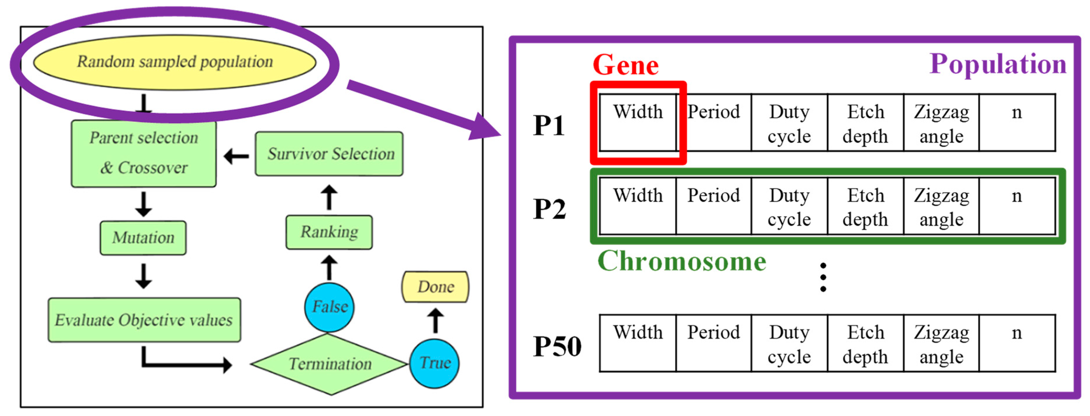
Figure 1 shows the flow diagram of the GA optimization algorithm. It begins with a set of individuals known as a population, as illustrated in the inset of
Figure 1. Each individual is a solution to the problem needed to be solved. An individual is symbolized by a set of parameters known as genes. Here, the width, period, duty cycle, etc. of the periodic zigzag structured mode converter are the genes. A set of parameters (all the genes) are grouped into a chromosome (the solution). Fitness functions are used to determine how fit an individual is, and the fitness function provides a fitness score to each individual. Here, we define the insertion loss of the device and mode extinction ratio (i.e., mode conversion efficiency) as the two fitness functions. Low insertion loss or high mode extinction ratio can provide high fitness scores. The insertion loss is defined in Equation (1), where
Pin and
Pout are the input and output optical powers of the SiPh device, respectively.
The mode extinction ratio is defined in Equation (2), where
PTarget-mode and
PInput-mode are the optical powers of the target mode and input mode to the SiPh device, respectively.
After the definition of the fitness functions, we select two parents randomly from the 50 individuals in the population and let them carry out crossovers. It is worth mentioning that the first two parents are selected randomly; after this, the two individuals (i.e., parents) are selected based on their fitness scores. This means that individuals with higher fitness will have a higher chance to be selected to reproduce. Crossover is an important process in the GA. For each pair of parents, a crossover point is chosen in the genes. Offspring are produced by the parents exchanging genes among themselves until the crossover point is reached. Here, 10 offspring generations are produced. Then, mutation occurs when new offspring are produced. Mutation occurs to maintain diversity within the population and prevent premature convergence. It is based on the Gaussian probability distribution. This means that the value in the gene can be mutated using the Gaussian distribution by adding a generated random value to it, resulting in a new mutated value. The mutation rate should be carefully tuned since it will degrade the device performance. It is also worth pointing out that the period number in the periodic zigzag structure should be an integer. After the mutation using the Gaussian distribution, the period number should be rounded off to the nearest integer. Then, we evaluate the objective values. This can be achieved by using the elitism GA or non-elitism GA. In the elitism GA, each pair of parents produces several offspring. All the individuals, including parents and offspring, are scored, and the low-fitness individuals are eliminated. On the contrary, in the non-elitism GA, each pair of parents produces two offspring, and all the parents are eliminated for the fitness selection. In this work, we use the elitism GA. Only the individuals with high fitness will survive, and we eliminate 10 individuals in each iteration. The algorithm terminates if the population has converged (i.e., it does not produce offspring which are significantly different from the last generation). Then, 50 new individuals will become the next population in the algorithm.
3. Design, Results and Discussion
All the mode conversion devices in this evaluation are based on a silicon-on-insulator (SOI) platform. The SOI wafer used has a silicon (Si) top layer of 220 nm and a silicon dioxide (SiO
2) burial oxide layer (BOX) of 2 μm.
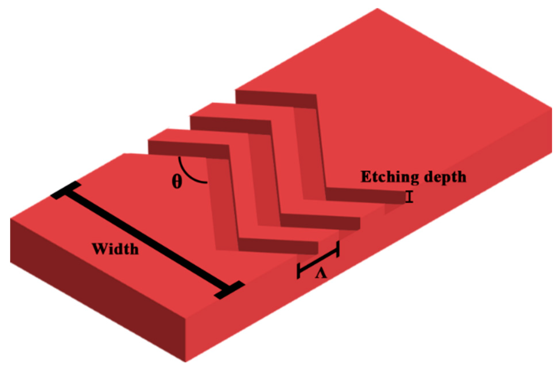
Figure 2 shows the schematic structure of a traditional periodic zigzag structured mode converter. The periodic zigzag mode converter is used as the reference for our proposed bulk mode converters later. Here, only the top Si layer is shown. It also illustrates the definitions of waveguide width, period, zigzag angle
θ and etch depth. The optimization is performed using the built-in Python API in Lumerical
®. After the optimization, the parameters are used by the Lumerical
® finite-difference time-domain (FDTD) method to simulate the SiPh device. After the implementation of the GA as described in the last section, the GA optimized periodic zigzag structured mode converter has the waveguide width and period number of 1.50 μm and 3, respectively. The period, duty cycle, etch depth and zigzag angle are 1.71 μm, 0.84, 0.07 μm and 34.97° respectively. These six parameters of the GA optimized TE
0 to TE
1 zigzag periodic structure mode converter are listed in
Table 1 and illustrated in
Figure 3a,b.
Figure 3c shows the FDTD simulation result of the periodic zigzag structured mode converter. The TE
0 mode can be successfully converted to TE
1 mode with a high transmission of 89.3% and low loss of 0.5 dB at the transmission wavelength of 1550 nm. The cross sections of the input TE
0 mode and the output TE
1 mode are illustrated in
Figure 3d and
Figure 3e, respectively.
Besides the TE
0 to TE
1 mode conversion, we also illustrate that the proposed periodic zigzag structure and the GA optimization can also support higher-order mode conversion. For brevity, we only describe the TE
0 to TE
2 mode conversion as illustrated in
Figure 4. The GA optimized periodic zigzag structured mode converter has the waveguide width and period number of 1.86 μm and 3, respectively. The period, duty cycle, etch depth and zigzag angle are 4.12 μm, 0.5, 0.077 μm and 53.34° respectively. These parameters of the GA optimized TE
0 to TE
2 zigzag periodic structure mode converter are also listed in
Table 2 and illustrated in
Figure 4a,b.
Figure 4c shows the FDTD simulation result of the periodic zigzag structured mode converter. The TE
0 mode can be successfully converted to TE
2 mode with a high transmission of 91.2% and low loss of <1 dB at the transmission wavelength of 1550 nm. The cross sections of the input TE
0 mode and the output TE
2 mode are illustrated in
Figure 4d and
Figure 4e, respectively.
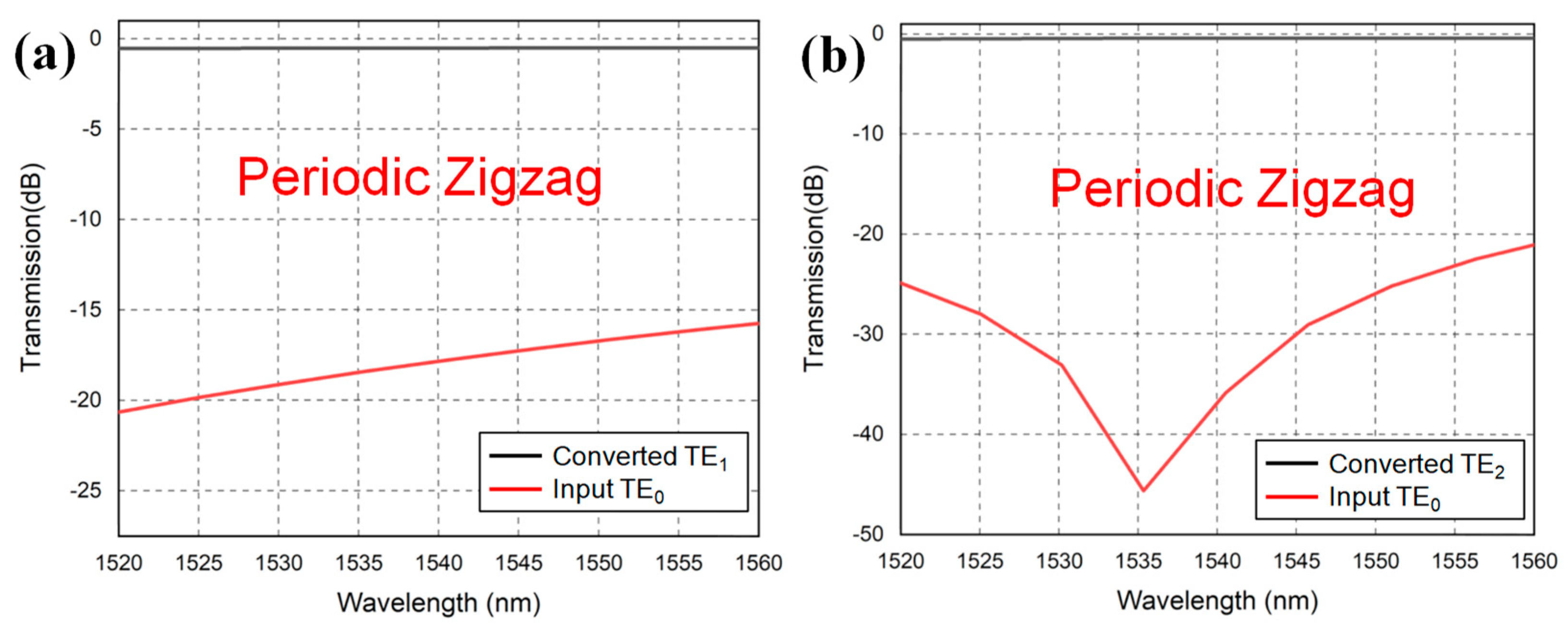
Figure 5a,b show the simulated mode conversion efficiencies (i.e., extinction ratio) between the target mode and the input mode of the TE
0 to TE
1 and the TE
0 to TE
2 periodic zigzag structured mode converters, respectively. The evaluation is performed in the wavelength window from 1520 nm to 1560 nm. For the TE
0 to TE
1 and TE
0 to TE
2 periodic zigzag structured mode converters, the mode extinction ratios are >15 dB and >20 dB, respectively, in the whole 40 nm wavelength range, illustrating a good mode conversion efficiency for the proposed SiPh device design optimized by GA optimization.
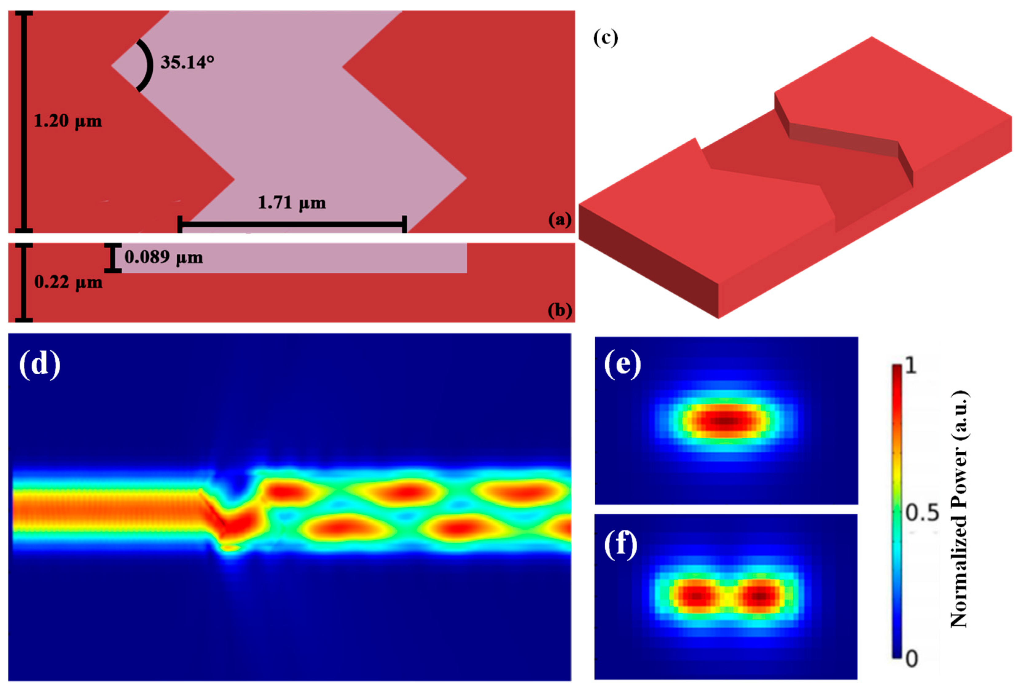
As discussed before, the periodic zigzag mode converter has many sharp zigzag angles in the periodic structure, which are very sensitive to the fabrication error. Here, we propose a bulk zigzag structure to achieve MDM mode conversion. There are only four parameters of the GA optimized TE
0 to TE
1 bulk zigzag structured mode converter and they are listed in
Table 3 and illustrated in
Figure 6a,b. The 3-D schematic of the bulk structure is shown in
Figure 6c. The waveguide width, bulk length, etch depth and zigzag angle are 1.20 μm, 1.71 μm, 0.089 μm and 35.14°, respectively.
Figure 6d shows the FDTD simulation result of the bulk zigzag structured mode converter. The TE
0 mode can be successfully converted to TE
1 mode with a high transmission of 86.9% and low loss of 0.48 dB at the transmission wavelength of 1550 nm. The cross sections of the input TE
0 mode and the output TE
1 mode are illustrated in
Figure 6e and
Figure 6f, respectively.
Similarly, we also perform the TE
0 to TE
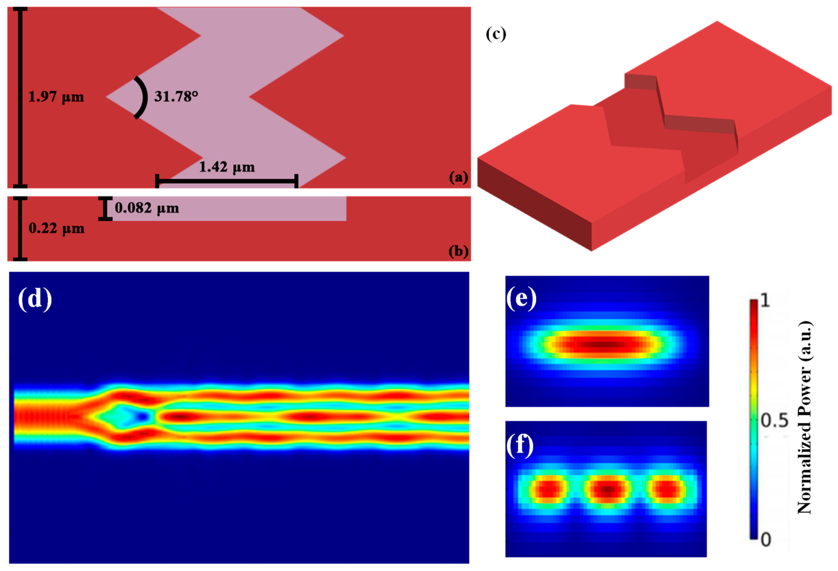
2 mode conversion. There are also four parameters of the GA optimized TE
0 to TE
2 bulk periodic structured mode converter which are listed in
Table 4 and illustrated in
Figure 7a,b. The 3-D schematic of the bulk structure is shown in
Figure 7c. The waveguide width, bulk length, etch depth and zigzag angle are 1.97 μm, 1.42 μm, 0.082 μm and 31.78°, respectively.
Figure 7d shows the FDTD simulation result of the bulk zigzag structured mode converter. The TE
0 mode can be successfully converted to TE
2 mode with a high transmission of 92.3% and low loss of 0.3 dB at the transmission wavelength of 1550 nm. The cross sections of the input TE
0 mode and the output TE
2 mode are illustrated in
Figure 7e and
Figure 7f, respectively.
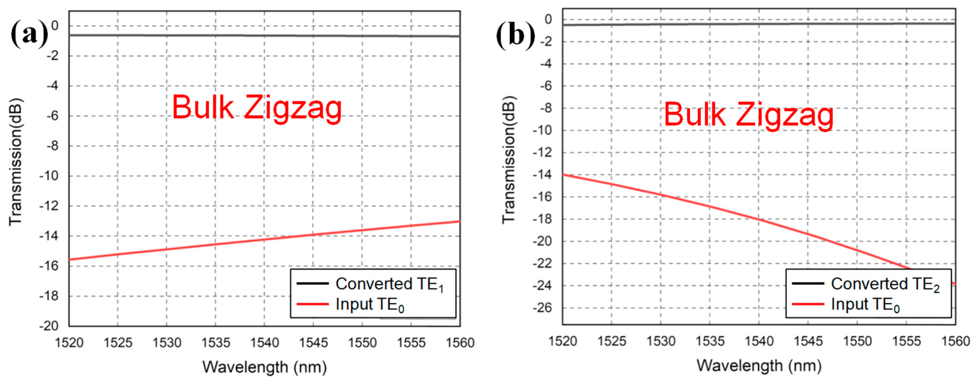
Figure 8a,b show the simulated mode conversion efficiencies between the target mode and the input mode of the TE
0 to TE
1 and the TE
0 to TE
2 bulk zigzag structured mode converters, respectively. The evaluation is performed in the wavelength window from 1520 nm to 1560 nm. For the TE
0 to TE
1 and TE
0 to TE
2 periodic zigzag structured mode converters, the mode extinction ratios are >12 dB and >14 dB, respectively, in the whole 40 nm wavelength range.
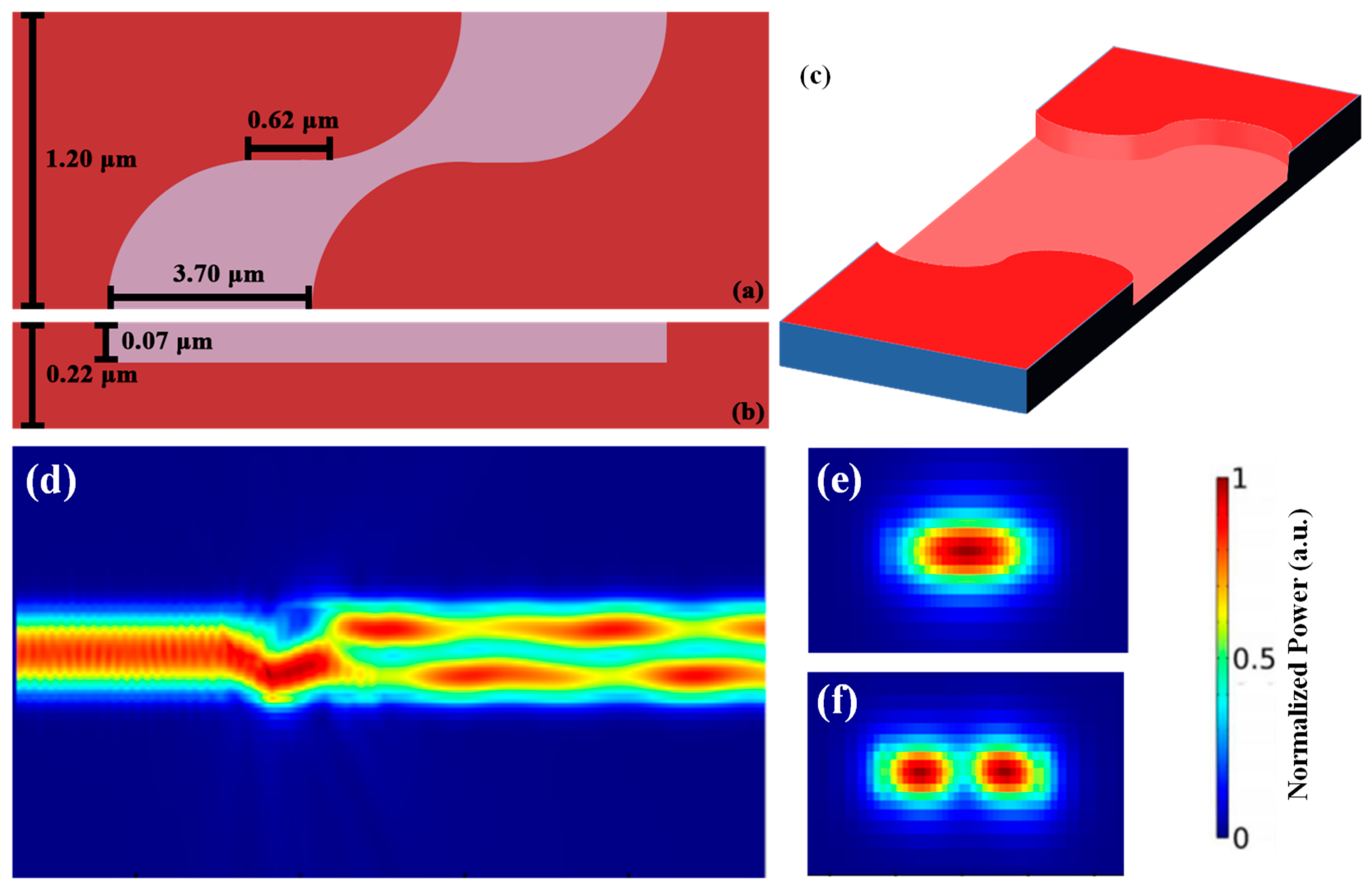
Finally, we further improve our device by using a bulk sinusoidal structure to further eliminate all the zigzag angles. As illustrated in
Figure 9a, the mode conversion region is composed of a half-period sine wave and a straight waveguide. The straight waveguide region is to prevent sharp bends between the sinusoidal functions. There are also four parameters of the GA optimized TE
0 to TE
1 bulk sinusoidal mode converter which are listed in
Table 5 and illustrated in
Figure 9a,b. The 3-D schematic of the bulk structure is shown in
Figure 9c. The waveguide width, bulk length, etch depth and straight waveguide length are 1.20 μm, 3.70 μm, 0.07 μm and 0.62 μm, respectively.
Figure 9d shows the FDTD simulation result of the bulk sinusoidal structured mode converter. The TE
0 mode can be successfully converted to TE
1 mode with a high transmission of 89.8% and low loss of 0.6 dB at the transmission wavelength of 1550 nm. The cross sections of the input TE
0 mode and the output TE
1 mode are illustrated in
Figure 9e and
Figure 9f, respectively.
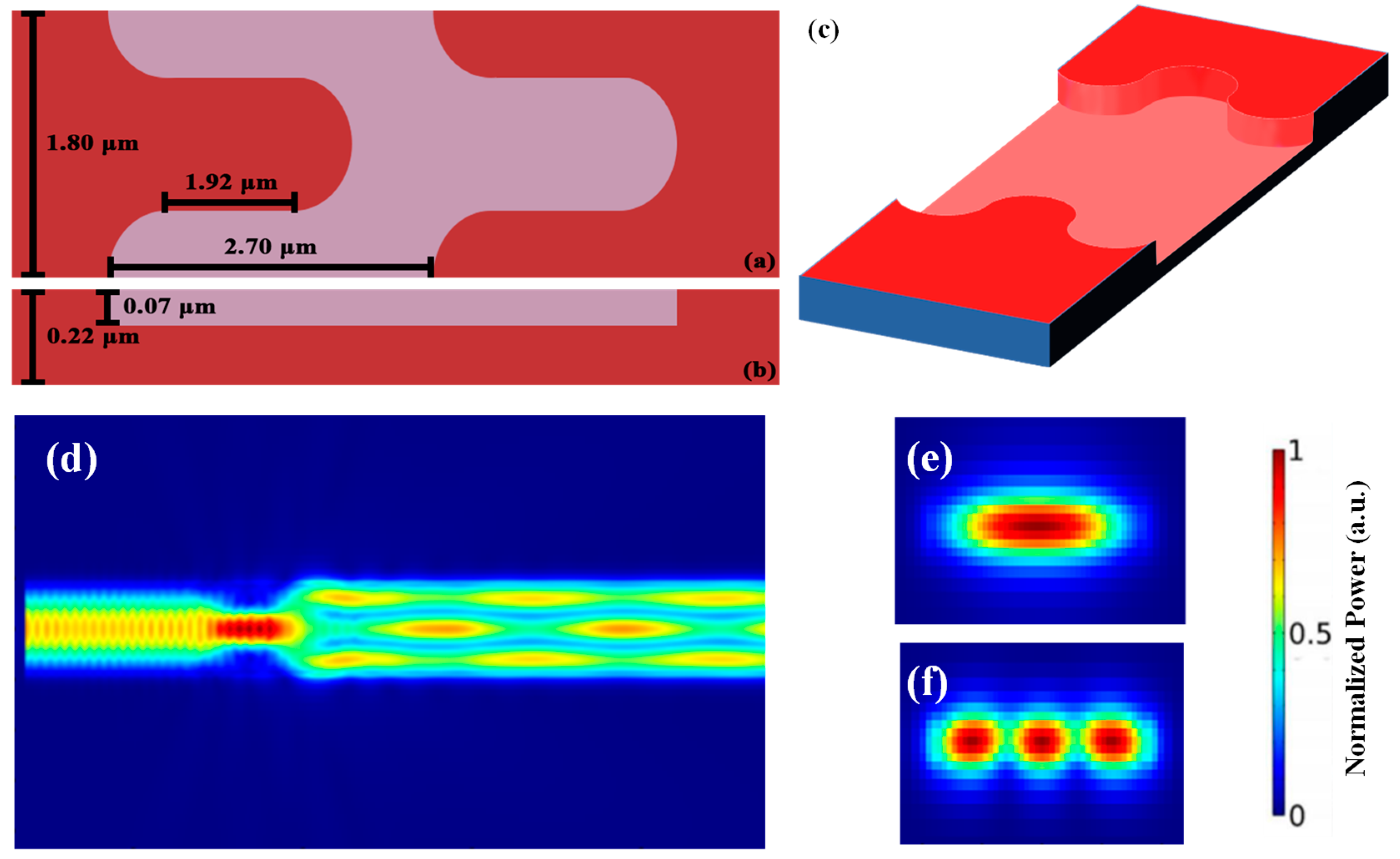
Similarly, we also perform the TE
0 to TE
2 mode conversion. There are also four parameters of the GA optimized TE
0 to TE
2 bulk sinusoidal structured mode converter which are listed in
Table 6 and illustrated in
Figure 10a,b. The 3-D schematic of the bulk structure is shown in
Figure 10c. The waveguide width, bulk length, etch depth and zigzag angle are 1.80 μm, 2.70 μm, 0.07 μm and 1.92 μm, respectively.
Figure 10d shows the FDTD simulation result of the bulk zigzag structured mode converter. The TE
0 mode can be successfully converted to TE
2 mode with a high transmission of 92.7% and low loss of 0.5 dB at the transmission wavelength of 1550 nm. The cross sections of the input TE
0 mode and the output TE
2 mode are illustrated in
Figure 10e and
Figure 10f, respectively.
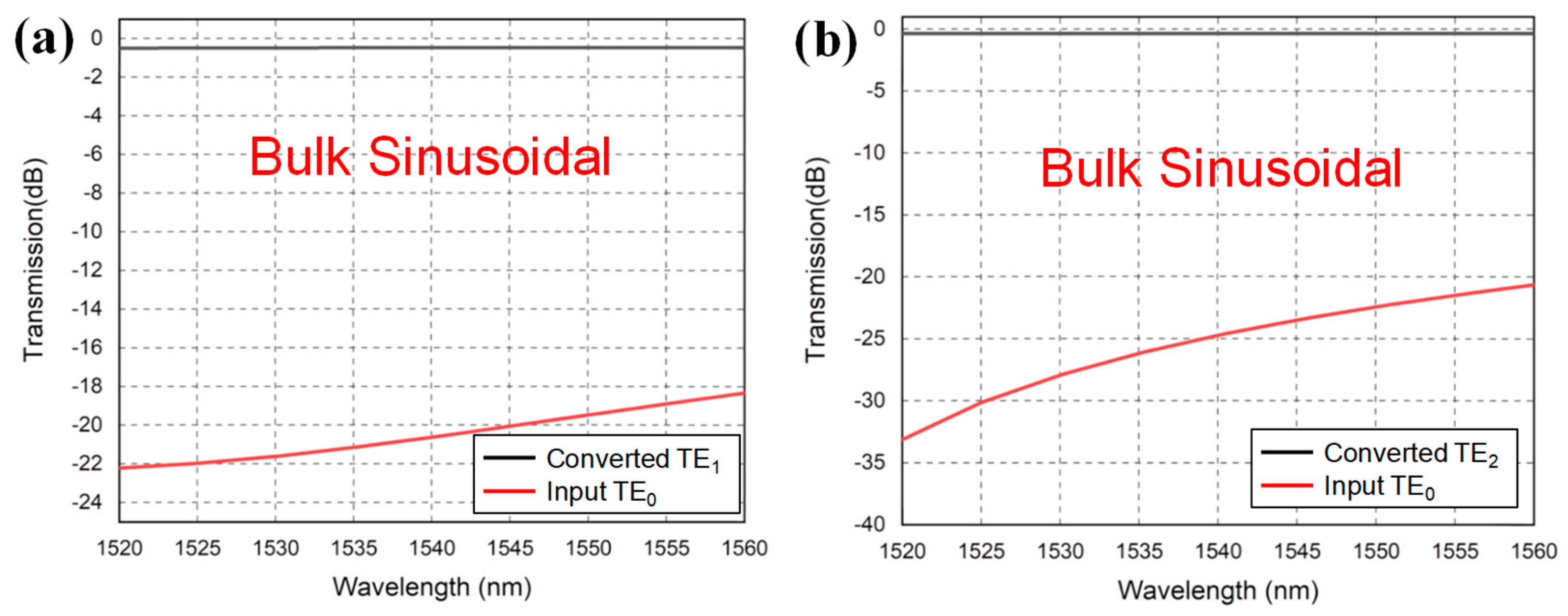
Figure 11a,b show the simulated mode conversion efficiencies (i.e., extinction ratio) between the target mode and the input mode of the TE
0 to TE
1 and the TE
0 to TE
2 bulk sinusoidal structured mode converters, respectively. The evaluation is performed in the wavelength window from 1520 nm to 1560 nm. For the TE
0 to TE
1 and TE
0 to TE
2 periodic sinusoidal structured mode converters, the mode extinction ratios are >18 dB and >20 dB, respectively, in the whole 40 nm wavelength range.
Table 7 summarizes the performances of the proposed bulk zigzag and bulk sinusoidal structured mode converters when compared with the traditional periodic zigzag mode converter. For the TE
0 to TE
1 mode converters, the three types of structures have transmission >86.9% and mode extinction ratio at 1550 nm wavelength >12.88 dB. We can observe a significant length reduction of the bulk zigzag and bulk sinusoidal structured mode converters, and their lengths are greatly reduced by 68% to 3.18 μm and by 32% to 6.78 μm when compared with the traditional periodic zigzag structured mode converter with length of 10.0 μm. For the TE
0 to TE
2 mode converters, the three types of structures have transmissions >91.2% and mode extinction ratio at 1550 nm wavelength >20.73 dB. Similarly, we can observe a significant length reduction of the bulk zigzag and bulk sinusoidal structured mode converters, as the lengths are reduced by 84% to 2.90 μm and by 81% to 3.48 μm when compared with the previous periodic zigzag structured mode converter with length of 18.5 μm. In addition, we can also observe that the proposed GA optimization can successfully be applied to all these SiPh structures under evaluation.
We also compare our proposed bulk sinusoidal mode converter with the popular traditional ADC-based mode converter [
25]. The simulated transmissions of the TE
0 to TE
1 and the TE
0 to TE
2 ADC-based mode conversions are >90% at 1550 nm wavelength, which are slightly higher than those of the proposed bulk sinusoidal mode converter. The mode extinction ratio of the ADC-based mode conversion is ~30 dB, which is also higher than that of the proposed bulk sinusoidal mode converter. However, the coupling lengths of the TE
0 to TE
1 and the TE
0 to TE
2 ADC-based mode are 17 µm and 22.5 µm, which are significantly longer than those of the proposed bulk sinusoidal mode converter, which are 3.70 µm and 2.70 µm, respectively.
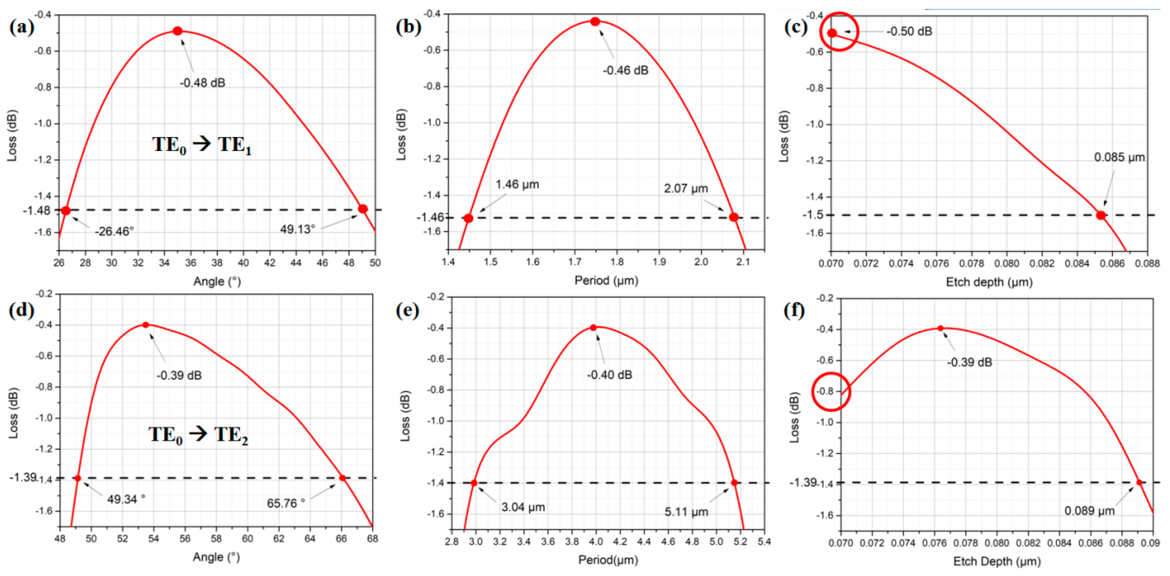
We also analyze the parameter tolerances for the six mode converters.
Figure 12a–f show the GA simulated loss against zigzag angle, period and etch depth for the TE
0 to TE
1 and the TE
0 to TE
2 periodic zigzag mode converters, respectively. It is worth noting that when a particular parameter varies around its optimized value, other parameters are fixed using the optimized values listed in
Table 1 and
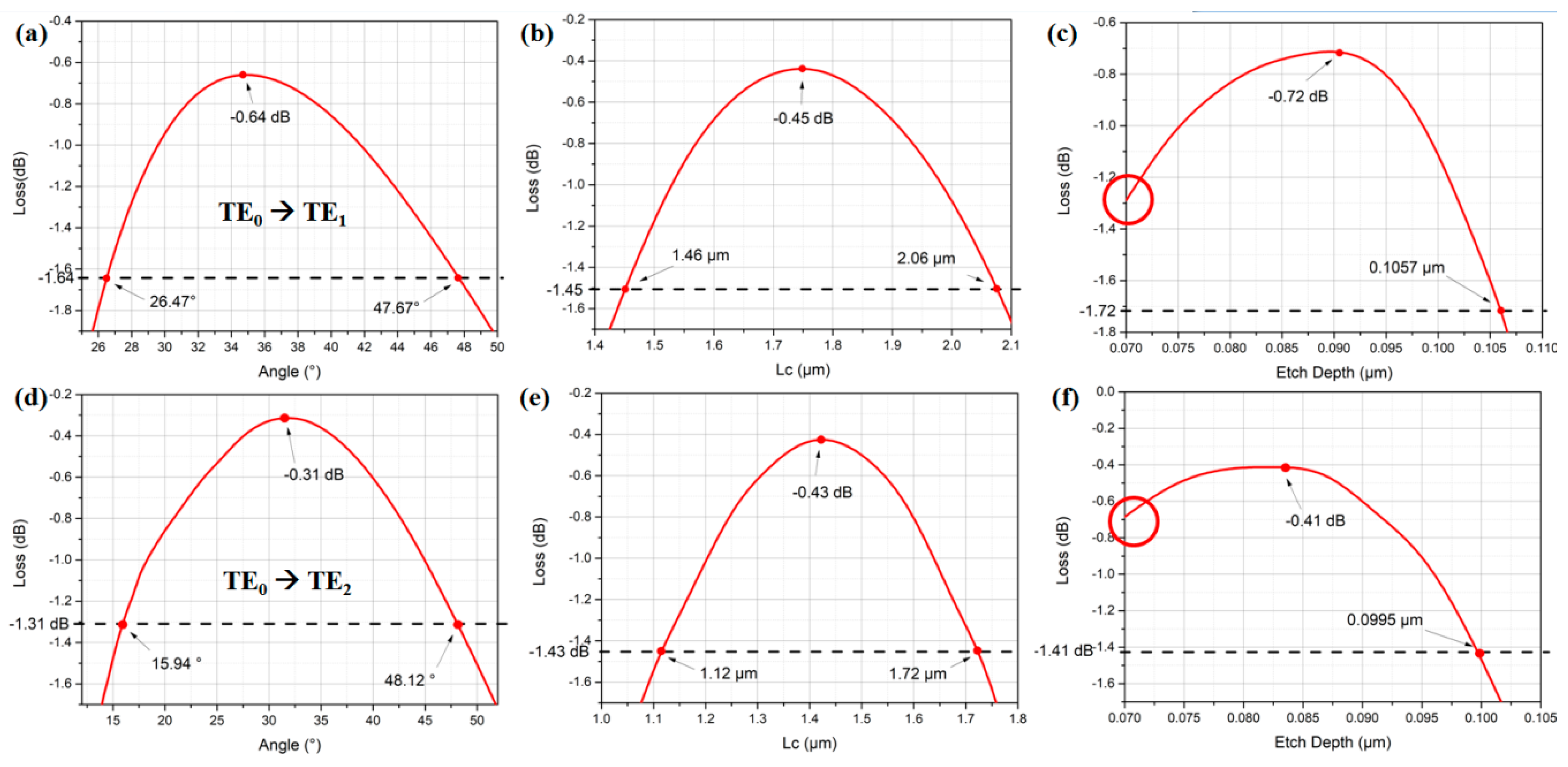
Table 2. Moreover,
Figure 13a–f show the GA simulated loss against zigzag angle, bulk length and etch depth for the TE
0 to TE
1 and the TE
0 to TE
2 bulk zigzag structured mode converters, respectively.
For the TE
0 to TE
1 mode conversion shown in
Figure 12a and
Figure 13a, we can observe that the zigzag angle tolerances in both periodic and bulk zigzag structures are similar. The −1 dB tolerances from the optimum values are ~20° in both devices. However, as the periodic zigzag structure has more zigzag angles than the bulk zigzag structure, the periodic structure could be more susceptible to fabrication error. For the TE
0 to TE
2 mode conversion shown in
Figure 12d and
Figure 13d, the −1 dB tolerance of the periodic zigzag structure is ~16°, while that in the bulk zigzag structure is ~32°. This shows the bulk zigzag structure is more robust against fabrication error.
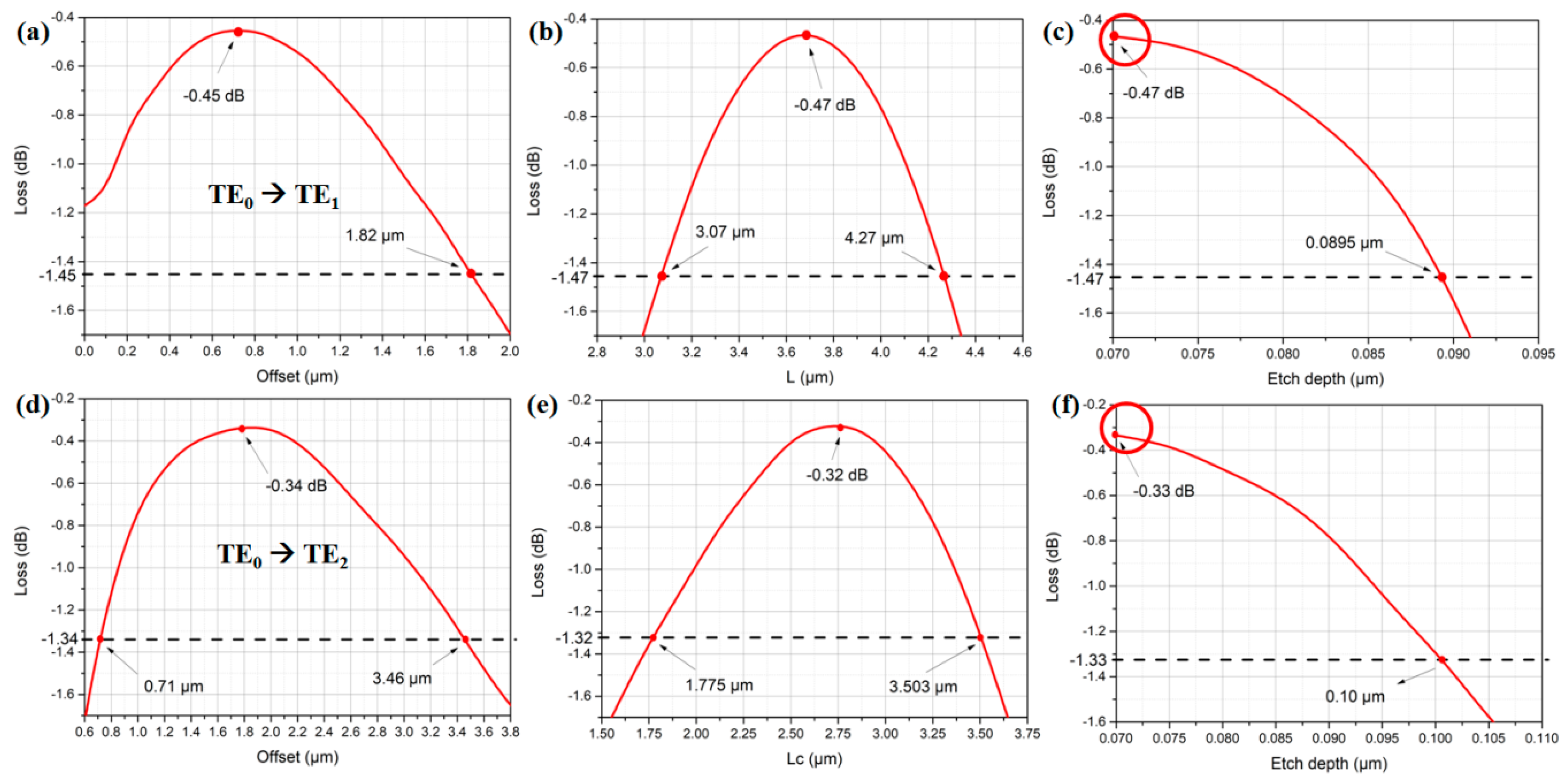
Figure 14a–f show the GA simulated loss against straight wavelength length (i.e., offset), bulk length and etch depth for the TE
0 to TE
1 and the TE
0 to TE
2 bulk sinusoidal structured mode converters, respectively. As shown in
Figure 12c,f,
Figure 13c,f and
Figure 14c,f, although the six mode converters have different optimized etch depths according to the GA simulation, we can still use the same etch depth for these devices to facilitate fabrication. We can observe that by fixing the etch depth to 70 nm for the six mode converters (i.e., the red circles shown in
Figure 12c,f,
Figure 13c,f and
Figure 14c,f), the losses are <1 dB in all six devices, illustrating that putting them on the same chip using the same etch depth is feasible.
