1. Introduction
In the mid-1860s, Maxwell established a complete theory of electromagnetic waves, and in the late 1880s, Hertz proved the existence of electromagnetic waves for the first time; in the late 1800s, Marconi discovered that light was an electromagnetic wave, and the difference in wavelength and frequency made electromagnetic waves take many forms. Since then, people have gradually become not satisfied with the discovery of more forms of electromagnetic waves but want to study how to artificially control the interaction between electromagnetic waves and matter, and thus the electromagnetic wave absorber was born. Traditional electromagnetic wave absorber devices have many problems, such as limitations caused by their quarter wavelength thickness, low absorption strength, narrow absorption bandwidth, etc., to be able to meet the design needs of today’s absorbers; with the development of nanofabrication technology, the concept of metamaterials has gradually been applied to the field of electromagnetic absorbers. Metamaterials are composite materials, artificial subwavelength structures rather than natural materials, with exotic properties not normally available in nature [
1]. Owing to their excellent properties, they have received a lot of attention and several applications have been suggested, including solar power generation [
2,
3], antenna systems [
4,
5], and electromagnetic stealth [
6]. Generally, according to absorption bandwidth, metamaterial absorbers can be grouped into two types: narrowband and broadband absorbers [
7,
8]. The former is frequently employed in thermal emitters and sensors [
9,
10] while the latter can be employed to realize solar energy harvesting [
11]. There are also absorbers with both narrowband and broadband absorption that make use of the refractive index change of phase and change materials at various temperatures to interconvert from broadband to narrowband absorption [
12,
13]. For this reason, several researchers have attempted to design absorbers with high absorption performance in the broadband case. Numerous absorbers with various structures for applications in the visible to near-infrared spectrum have been suggested, including the solar absorber [
14]. Due to the strong solar radiation energy under the visible to near-infrared (NIR) band (400–2500 nm), having a strong absorption under this band can significantly absorb the energy of sunlight; for example, Lei et al. suggested a visible to NIR absorber consisting of Ti cubes as the top layer structure which can attain more than 90% absorption in the continuous spectral range of 354–1066 nm [
15]. A new option could be the addition of SiO
2 as an anti-reflection layer to extend the absorption bandwidth in the NIR region. An ultra-broadband polarization-independent metamaterial absorber was suggested by Liu et al. in the literature [
16] which, using MgF
2 as a dielectric layer and SiO
2 as an anti-reflection layer, can attain more than 90% absorption at 405–1505 nm. Liao et al. proposed a six-layer, wide-angle polarization-insensitive ultra-wideband absorber using tungsten (W) and calcium fluoride (CaF
2), and the simulation results showed an absorbance greater than 0.9 at normal incidence in the wavelength range of 400–1639 nm [
17]. However, these suggested ultra-wideband absorbers also have some limitations, such as an inadequately long absorption bandwidth (defined as >90% absorption) or low peak or average maximum absorption which are crucial factors in assessing whether the absorber quality is good.
Based on this, a polarization-independent solar broadband absorber with near-perfect absorption over a wide range of incidence angles is designed and numerically analyzed in this study. The designed structure is a novel ultra-broadband absorber based on a four-layer structure of silicon dioxide–iron–magnesium fluoride-chromium (SiO2-Fe-MgF2-Cr), and its near-perfect absorption performance in the visible and NIR is exhibited using numerical calculations. The top two layers are an array of SiO2 and Fe square rings, whereas the last two layers are MgF2 and Cr flat film. With maximum absorption of 99.6% and an average absorption of 98.6%, the designed absorber attains an optical absorption of more than 90% in the wavelength range from visible to near-infrared (NIR) (496–2100 nm). The effect of various physical materials and structural parameters on the absorption performance of the absorber designed in this study is also analyzed in detail. Furthermore, we show that the absorber is incidence-angle-insensitive and polarization-independent and plot the electromagnetic field’s intensity distribution at certain absorption peak positions, which is used to show the physical mechanism underlying this effect. The electromagnetic fields indicate that propagating surface plasmon resonances (PSPR), localized surface plasmon resonances (LSPR), and resonances of the Fabry–Perot (F-P) cavity are substantially excited in the novel absorber suggested in this study. We also show that the suggested multilayer metamaterial structure can function as a near-perfect absorber in terms of performance and that such high absorption rates are the effect of combining the resonances of the PSPR, LSPR, and FP cavities. The LSPR effect is excited at the edges of the metal. The square ring design allows the LSPR effect to occur simultaneously at the inner and outer edges, and the electric field coupling between the inner and outer rings further increases the absorption. Finally, to evaluate its potential application in solar energy harvesting and conversion, the absorber’s absorption properties are examined in the solar radiation spectrum at an atmospheric mass of 1.5 (AM 1.5).
2. Structural Design with Ultra-Broadband Absorbency
Figure 1a plots the scheme of the designed structure, and it is worth noting that the structure in the x–y plane of
Figure 1a comprises an infinite number of cells.
Figure 1b depicts the structure of a cell with an array period of
. The side lengths of the outer and inner rings of the square ring are
and
, respectively, and the thicknesses of the SiO
2, Fe resonant ring array, MgF
2 spacer region, and Cr substrate are
,
,
, and
.
Figure 1c shows the appearance of the side view of the designed absorber. The suggested structure combines the excitation of PSPR, LSPR, and resonance of FP cavities to attain a near-perfect absorbance in the visible to NIR band (496–2100 nm), as will be exhibited in this study.
To construct models and simulate the computation of electromagnetic waves, the Finite Difference Time Domain (FDTD) method is a technique of numerical analysis that can be employed and has been used to simulate the optical properties and absorption rates of designed ultra-broadband absorbers. It solves Maxwell’s equations, ensuring the dependability and precision of numerical results for numerous studies. After the FDTD method to compute the absorption spectra and optimize the structure’s parameters in this study [
18,
19,
20,
21,
22,
23], Lumerical FDTD 2023 R1 is used for all numerical simulations in this paper.
As shown in
Figure 1d, we set the perfect match layer (PML) boundary conditions (black squares) at the top and bottom of the
z-axis direction to ensure the correct truncation of the electromagnetic field. Periodic boundary conditions (blue dashed lines) are set in the x and y directions to simulate an array structure of infinite cells. The computational grid accuracy is set to 5 nm (red dotted line). A light source is placed at 1500 nm above the cell structure, and the wavelength range of the light is set to 400–2100 nm. A frequency domain field and a power monitor (yellow square) are also placed 500 nm above the light source and 500 nm below the structure. The electromagnetic waves reflected back by the structure or partially transmitted through the structure will be picked up by the monitor and used to calculate the reflectance and transmittance of the structure, respectively. The refractive indices of SiO
2 and MgF
2 are set to 1.45 and 1.38 [
24], assuming that the surrounding material is air. The composite dielectric constants of Fe and Cr metals were obtained by Drude–Lorentz fitting. In addition to utilizing the properties of the material itself, the resonant wavelengths and absorption effects in the metamaterial absorber depend heavily on the shape and geometry of the top pattern [
25,
26,
27]. The absorption
can be denoted as
, where
denotes reflection and
represents transmission. In this metamaterial structure, the absorber
can be approximated to zero since the Cr substrate at the bottom is thick enough (250 nm), and the reflectance can be obtained using a power monitor set above the light source. The absorptance of this absorber can thus be computed from
.
The optimal geometrical parameters were finally obtained after calculating the absorption spectra using the FDTD method and optimizing the structure’s parameters in this study to period = 380 nm, square inner ring edge length = 160 nm, square outer ring edge length = 270 nm, and the thickness of each layer was = 130 nm, = 50 nm, and = 140 nm, = 250 nm.
3. Results and Discussion
Narrowband absorbers require sharp absorption peaks for selective high-level absorption in a specific narrow band. Sharp absorption peaks give narrowband absorbers higher sensitivity in sensor applications while broadband absorbers require nearly uniform and efficient absorption in a specific wide band. A uniform and high level of absorption helps the absorber to absorb electromagnetic waves in a specific wide band with almost no loss.
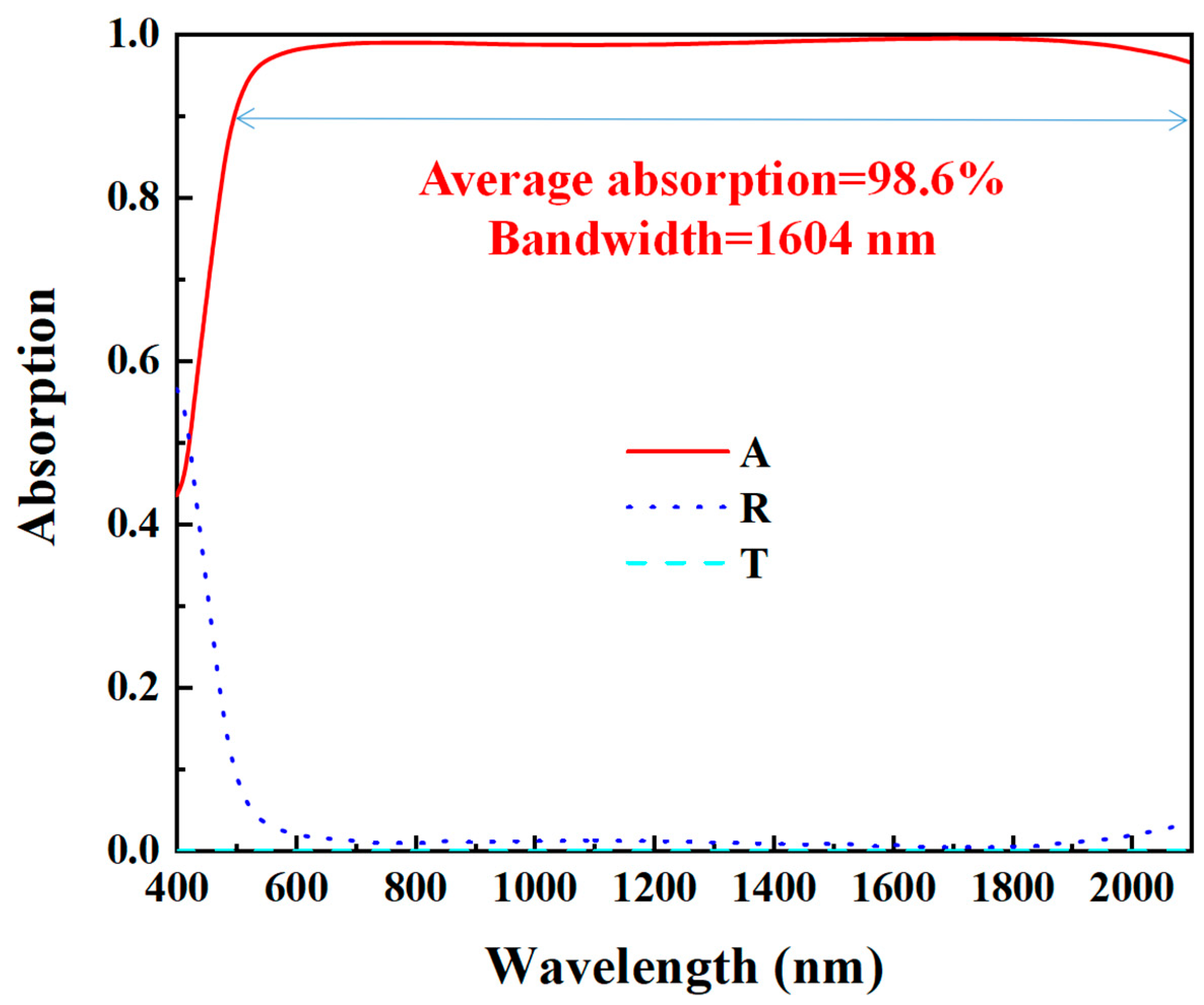
Figure 2 presents the performed numerical simulations of the Absorption (A), reflection (R), and transmission (T) spectra in normal TE incident light. The absorber has a continuous high absorption (>90%) in the ultra-broadband range of 496–2100 nm as can be observed; transmittance is near zero, and the findings indicate that the designed absorber has a bandwidth of up to 1604 nm. In the range of 496–2100 nm, the maximum absorbance was 99.6%. The average absorbance was 98.6% which could be calculated as follows:
where
is 496 nm and
is 2100 nm. To explain the physical mechanism of the examined absorber with high absorbance in the visible to NIR band (496–2100 nm), electromagnetic fields are commonly used in the analysis of physical mechanisms to explain the strong interaction of absorbers with electromagnetic waves] [
28,
29,
30,
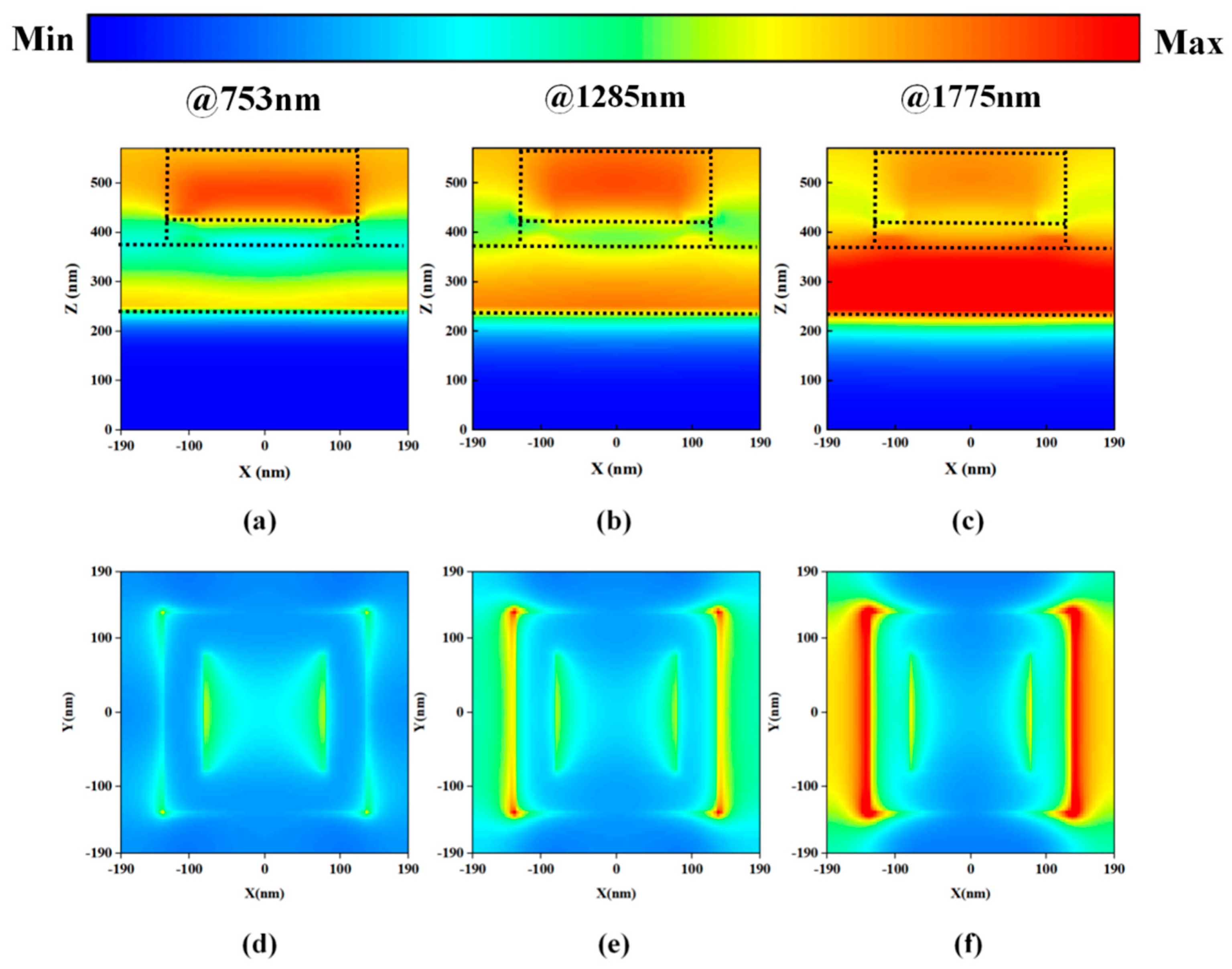
31]. Since the electric field is mainly concentrated on the metal surface and the magnetic field occurs internally, we calculated the distribution of the electric field intensity (|E|) in the x–y plane and the magnetic field intensity field (|H|) in the x–z plane, and these absorption peaks are proportional to the incident TE light with wavelengths of 753, 1285, and 1775 nm.
Figure 3a–c shows the magnetic field (|H|) distributions for incident light wavelengths of 753, 1285, and 1775 nm, respectively. When the light wavelength is 753 nm, a relatively strong magnetic field appears at the edge of the square iron ring, indicating that the LSPR effect is excited. When the wavelength of light increases to 1285 nm, it passes through the interior of the iron ring, and a stronger magnetic field appears at the junction of the iron ring and the MgF
2 layer as well as inside the MgF
2 layer; meanwhile, the surface PSPR effect is excited [
32]. Furthermore, owing to the nature of the metal–insulator–metal (MIM) structure, a relatively weak F-P cavity resonance occurs inside the MgF
2 layer. A conventional F-P cavity can comprise two mirrors (generally they are the same or distinct metals) and due to the high reflectivity of the upper and lower parts, the incident electromagnetic energy can be reflected front and back in the cavity, therefore, improving the optical radiation energy’s absorption. Thus, by observing the magnetic field intensity distribution on the MgF
2 dielectric layer, the presence of FP cavity resonance can be observed. When the light wavelength reaches 1775 nm, the PSPR at the junction of the Fe ring and MgF
2 layer and the F-P cavity resonance inside the MgF
2 layer is further improved. We can observe that
Figure 3d–f below demonstrates the electric field intensity (|
E|) distribution at various wavelengths of normal incident TE polarized light, depicting that the light is coupled to the Fe square ring’s edges and the electric field intensity at the edges increases as the wavelength of light increases. When the artificial metallic structure on the material surface is smaller than the incident electromagnetic wave’s wavelength, the surface plasmonic excitations generated in the presence of the incident electromagnetic wave are confined and improved near the metallic structure to form LSPR excitation [
33]. Thus, the electric field diagram depicts that the LSPR effect is substantially excited on the Fe ring’s edge, and the absorption is further improved by the field coupling that occurs between the two square rings because of the small spacing between the inner and outer square rings. The maximum effect is attained when the light wavelength is 1775 nm and when the absorption reaches a perfect absorption of 99.6%. Summarily, the LSPR resonance occurs at 753 nm and the structure undergoes LSPR and weak FP and PSPR resonance when the wavelength is increased to 1285 nm. The perfect absorption at 1775 nm is caused by the combination of the resonance of the PSPR, LSPR, and F-P cavities, with the PSPR and LSPR playing a stronger role. The structure has an extremely flat and efficient absorption due to the combined superposition of the PSPR and LSPR effects and the strong excitation of the FP cavity resonance at multiple resonance wavelengths.
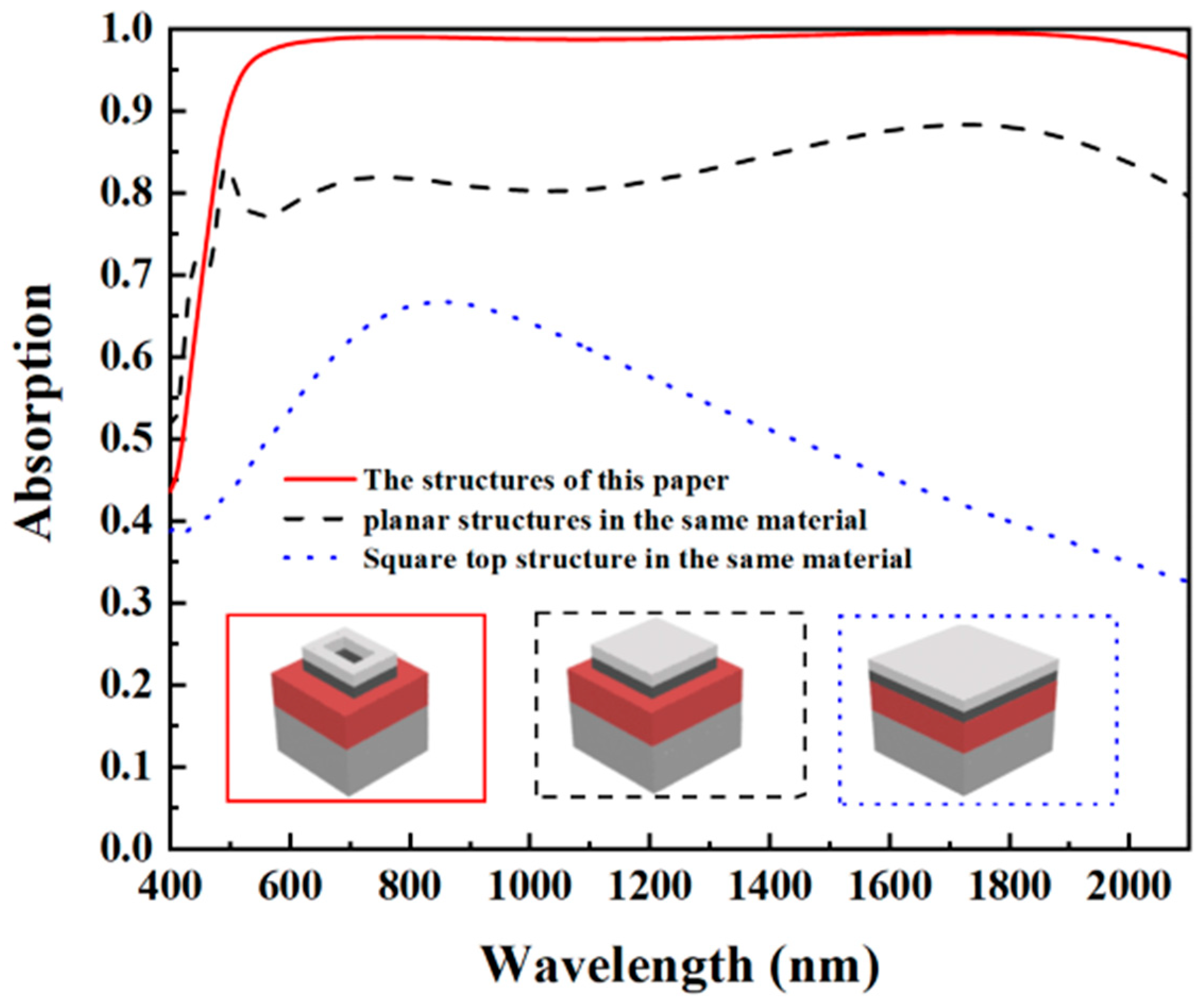
The novel ultra-broadband absorber was compared to flat film and square top structures with the same material and thickness of the same material structure to further show the superiority of this structure, as shown in
Figure 4. The ultra-broadband absorber’s absorption with a square Fe ring is much greater than that of flat film and square top structures with the same material, and only the PSPR and F-P cavity resonances occur in the flat film structure at 753 nm. The absorption of the flat film structure is lower since its intensity is much less than the strong absorption effect brought about by the LSPR resonance effect. In
Figure 5, the absorber with the SiO
2 antireflection layer absorbs light in the visible range drastically better than the absorber without the SiO
2 antireflection layer, therefore showing that the SiO
2 antireflection layer does have an improved absorption effect in the visible band, which is extremely crucial owing to the particularly intense radiant energy of light in the visible range.
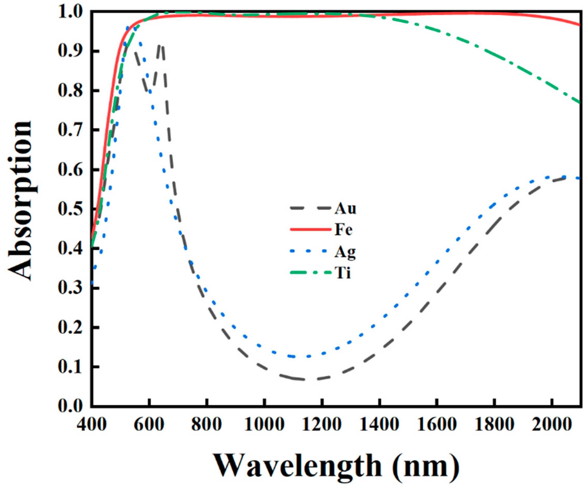
Figure 6 depicts the comparative absorption profiles for various top metal materials with structural changes in this study. It can be observed that the absorption using the precious metals gold (Au) and silver (Ag) as top metal materials only has a narrow band absorption peak in the visible range, which is far from broadband absorption. Ti is presently the more common top layer metal material. We can observe that by comparing the absorption under two top-layer metal materials Fe and Ti, Ti as the top-layer metal material has a slightly higher absorption than Fe in the 500–1200 nm band, but the absorption bandwidth is much smaller than the absorption bandwidth under Fe as the top-layer metal material. Thus, the use of Fe as the top metal is more appropriate for impedance corresponding to the structure of this study.
In addition, to demonstrate that the structural parameters have been optimized, we also investigated the effect of various structural parameter variations on the absorption performance of the proposed absorber. As shown in
Figure 7, the absorption intensity in the visible to near-infrared band for a certain range of variations of each parameter was scanned by the FDTD algorithm, and the obtained results were plotted as spectra, with the red dashed line depicting the absorption intensity of the structural parameters in this study.
Figure 7a shows the scanning spectra of SiO
2 thickness. The thickness
of the SiO
2 antireflection layer is selected to vary in the range of 50–200 nm. When
= 50 nm, the absorber has a strong absorption only in the NIR region, and as
increases, the absorption peak in the visible region gradually appears, and when
reaches 130 nm, there is a strong absorption in the visible to NIR band with the maximum bandwidth; h increases further, making the absorption peak red-shifted and hindering the absorption of the visible part.
Figure 7b shows the absorption intensity spectra of the absorber Fe layer thickness
varying in the range of 20–80 nm. When
= 20 nm, the absorption intensity is extremely low; when
increases to 30 nm, the absorption peaks in the visible region gradually appear; as
increases further, the absorption peaks in the NIR region appear one after another. When
= 50 nm, the absorber absorbs the best; at this time the absorber shows nearly uniform absorption intensity in the visible to NIR band. When
continues to increase, the absorption peaks are red-shifted and the absorption peaks in the visible region gradually disappear.
Figure 7c shows the absorption spectrograms of the spacer layer MgF
2 thickness
varying in the range of 110–200 nm, and the absorption effect is best when
= 140 nm and the absorption intensity is almost uniform.
Figure 7d,e shows the scanned spectrograms of the inner and outer edge lengths of the square ring
and
, respectively, with the best absorption when
= 160 nm and
= 270 nm. When
continues to increase, the absorber shows slightly enhanced absorption in the visible region and substantially weaker absorption in the near-infrared region. When
continues to increase, the absorption in the near-infrared region is slightly enhanced and has a substantially weaker absorption in the visible region. In order to make the absorber have a nearly uniform and high-level absorption effect, take
= 160 nm and
= 270 nm.
Figure 7f shows the absorption spectrum graph of the square ring array period p varying in the range of 320–440 nm. When the period
is greater than 350 nm, the absorption peak is gradually revealed; when
= 380 nm, the absorption effect is the best. If
continues to increase, it can be found that the bandwidth of the absorber gradually decreases, and the absorption mainly in the near-infrared light region gradually decreases. In summary, the proposed absorber structure obtained the best absorption at
= 130 nm,
= 50 nm,
= 140 nm,
= 160 nm,
= 270 nm, and
= 380 nm.
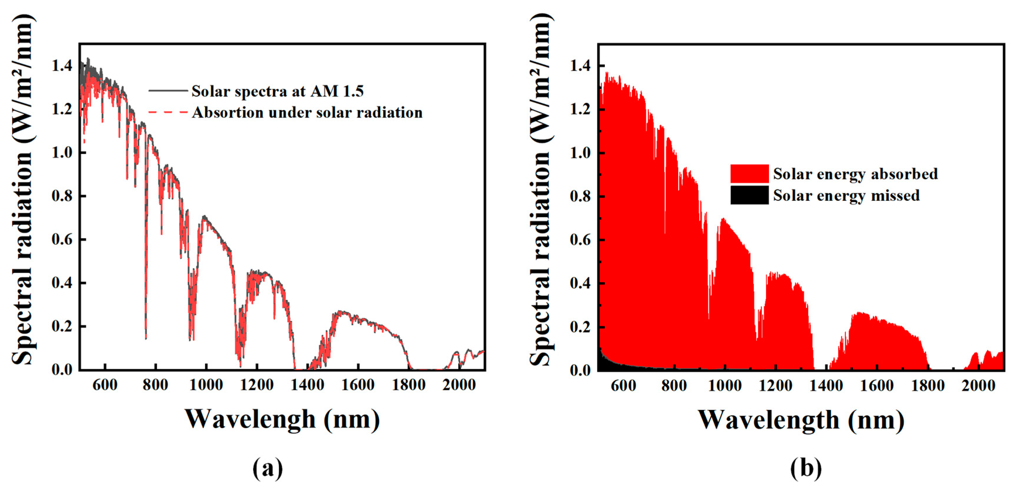
Finally, to assess the structures’ potential application for solar energy capture, we computed the absorption of solar radiation in this study using the structures in the AM 1.5 spectrum. The solar radiation energy of AM 1.5 was compared to the absorption of solar radiation energy of AM 1.5 by the absorber and used to evaluate the absorption efficiency of the absorber at the solar radiation band [
34,
35].
Figure 8a shows that most of the solar radiation energy from the AM 1.5 spectrum was discovered to be concentrated in the visible and NIR regions. Thus, to enhance the performance of solar energy collection, the absorption in these regions should be enhanced.
Figure 8b shows the absorption and loss of AM1.5 solar radiation by the absorber, and it can be seen that there is only a small loss of visible light, and the rest is nearly perfectly absorbed. As depicted in
Figure 2 and also as described above, the designed absorber exhibited an average absorption of about 98.6% in the spectral range of 496–2100 nm. Thus, the designed structure should have a substantial solar absorption capacity. This is again confirmed using the absorption spectra under solar radiation depicted in
Figure 8a, where the black solid line denotes the solar radiation energy at AM 1.5 and the red dashed line represents the absorption of the solar radiation energy at AM 1.5 by the structure suggested in this study. It can be observed that the structure designed therein is consistent with the spectrum of AM 1.5. The structure can thus be used for applications in the direction of high-performance solar energy harvesting, including solar energy capture and conversion, solar power generation, thermal emitters, etc.
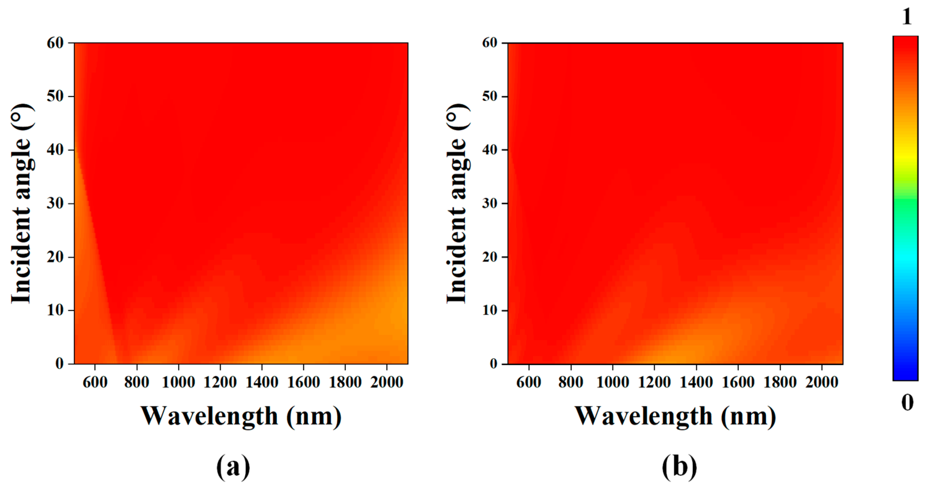
Furthermore, in practical applications, broadband absorption properties require to be maintained over a wide range of incidence angles.
Figure 9 depicts the absorption evolution spectra for incident angles from 0° to 60° under TE and TM polarized light conditions. To evaluate the designed structure’s angular sensitivity, the variation of the absorption profile with varying incidence angles at various wavelengths was computed for both TE and TM polarization conditions. The absorption is slightly lower in the spectral range 1300–2100 nm at angles of incidence below 10° but also remains close to 90% for the TE polarization in
Figure 9a. Then, with a further increase in theta, the absorption exceeds 90% for all absorbers below an incidence angle of 60°. As depicted in
Figure 9b in comparison, at low incidence angles, the TM polarization only demonstrates lower absorption in the 1200–1500 nm band range, with the rest performing well at the given incidence range. Furthermore, a good spectral overlap between the absorption of the two polarizations was discovered with an increasing incidence angle, demonstrating the polarization-independent and broadband large-incidence-angle absorption properties of the structures in this study.

