Article

Photonic-Enabled Image Rejection Mixer with Simultaneous Wideband Self-Interference Cancellation for In-Band Full-Duplex System

1
College of Information and Navigation, Air Force Engineering University, Xi’an 710077, China
2
Key Laboratory of Electronic Information Control, Southwest China Research Institute of Electronic Equipment, Chengdu 610036, China
*
Authors to whom correspondence should be addressed.
Photonics 2023, 10(6), 657; https://doi.org/10.3390/photonics10060657
Submission received: 6 April 2023 / Revised: 18 May 2023 / Accepted: 3 June 2023 / Published: 6 June 2023
(This article belongs to the Special Issue Signal Processing and Transmission Enabled by Microwave Photonics)

Abstract

:
In this paper, a photonic-enabled image rejection mixer (IRM) that features an ultrawideband self-interference cancellation (SIC) function and a compact configuration is proposed. The parameter tuning of SIC is realized in an optical domain, which avoids the use of electrically tuned devices with limited bandwidth and precision, so that high-precision parameter matching can be realized in the optical domain to realize deep and ultrawideband SIC. The key point of image rejection (IR) is to construct a pair of orthogonal local oscillation (LO) signals through DC-bias-induced phase shift. This not only avoids a high-frequency electrical 90-degree hybrid coupler (HC) applied in the traditional Hartley structure, but also compensates the phase deviation in the electrical intermediate frequency (IF) 90-degree HC flexibly, ensuring wideband and deep IR operation. The simulation results show that the proposed IRM can achieve ultrawideband SIC and IR with the simultaneous high-efficiency recovery of useful signals. They also verify that the scheme has good resistance to strong interference, and can cope with the phase imbalance of the IF 90-degree electrical HC, ensuring the good performance of the system, which has a wide application prospect in various in-band full-duplex (IBFD) systems.

1. Introduction

In recent years, the development of microwave photonic technology, which combines the advantages of flexible access in the microwave field and fine regulation in the optical field, has attracted wide attention in various fields [1,2]. Compared with traditional electrical technology, microwave photonic technology features broadband operation ability, electromagnetic immunity and optical fiber transmission compatibility, as well as small size, light weight and low transmission loss [3,4]. In a typical example of applying microwave photonic technology to realize a variety of signal processing functions, frequency mixing is an essential function and has great application value [5]. Specifically, converting high-frequency signals down to intermediate frequency (IF) is particularly helpful in reducing the sampling rate requirements for the subsequent analog-to-digital (ADC) conversion and digital signal processing (DSP) [6]. In addition, the combination of microwave photonic technology and in-band full-duplex (IBFD) systems can provide full play to the parallel processing capability and wideband multi-dimensional parameter tuning capability of photonics, as well as the high-spectrum utilization efficiency of IBFD technology, thus becoming a typical example to solve the contradiction between limited spectrum resources and high data rates [7,8]. Therefore, photonic-enabled in-band full-duplex frequency down-conversion systems have gained great attention in RF transceivers for wireless communication systems, radar frontends and satellite payloads [9]. However, an urgent problem to be solved in the IBFD frequency down-conversion system is the disturbance of in-band interference containing unwanted image interference and self-interference [10,11]. Image interference and self-interference (SI) will inevitably be captured by the antennas of RF transceivers. These two kinds of in-band interference will be spectral-aliased with the desired IF signal after mixing with the local oscillation (LO) signal, which leads to the distortion of the desired IF signal. Therefore, an image rejection mixer (IRM) with a self-interference cancellation (SIC) ability is the key to effectively solving the Gordian knot and achieving efficient signal sending and receiving.
Previously, several photonics-based schemes to eliminate these two kinds of in-band interference have been demonstrated [12,13,14,15], which are very instructive. However, the SIC function in Refs. [12,13] was realized by virtue of electrical components to achieve time delay and amplitude matching between SI and reference signals. Since the cancellation depth is greatly affected by the time delay and amplitude matching, the SIC performance based on electrical components lags behind schemes applying optical devices with high tuning precision due to its limited tuning accuracy [16]. In Refs. [14,15], electrically tuned devices were avoided, thus guaranteeing the wideband deep cancellation of SI and image interference. However, there are many tuning devices and several discrete paths in Ref. [14]. It has four independent paths that need to be tuned and matched, not only increasing the difficulty of parameter tuning but also increasing the complexity, which is not conducive to practical applications. In Ref. [15], an incoherent optical system was applied, which inherently limits the compactness and simplicity of the system [17]. Therefore, an IRM with simultaneous SIC features of ultrawideband operation, deep cancellation and compact configuration is desired for practical applications.
In this paper, a photonic-enabled IRM with simultaneous ultrawideband SIC is proposed. It is constructed in a single optical path structure based on a coherent optical source. The phase reversion and amplitude matching of SIC operation are realized by using optical polarization regulation, and the time delay matching is realized by using an optical high-precision time delay device, making SI directly canceled in the optical domain. A pair of orthogonal LO signals can be constructed by controlling the phase shift introduced by the DC bias without requiring a bandwidth-limited high-frequency electrical 90-degree hybrid coupler (HC) so that the wideband image rejection (IR) operation can be achieved through the typical phase cancellation method. This scheme not only avoids the use of high-frequency electrical devices with limited tuning precision and bandwidth, but also simplifies system complexity. Therefore, the SI and image interference can be simultaneously canceled in a compact configuration. Its application can promote high-efficiency communication under the strong interference of the IBFD system.

2. Principle

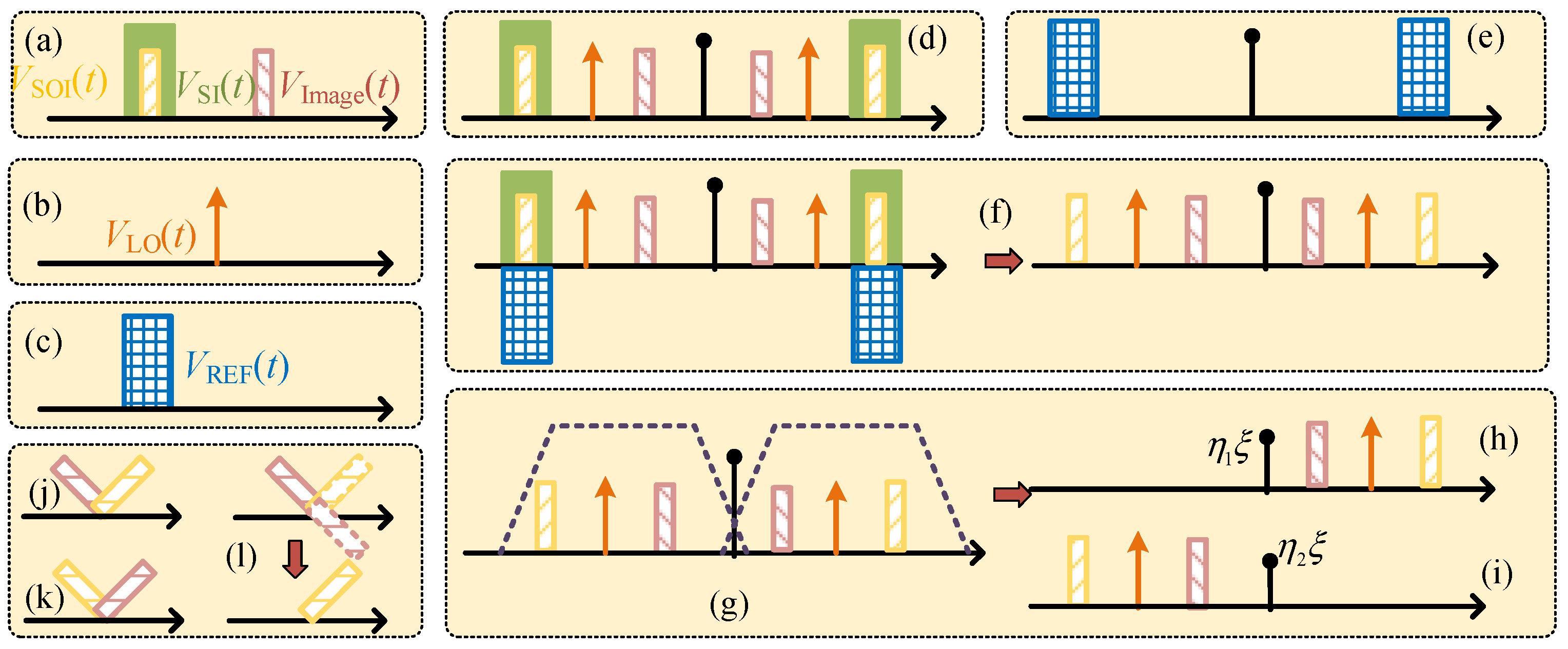
Figure 1 shows a schematic diagram of the proposed IRM with simultaneous SIC. A coherent optical structure based on a main polarization-division-multiplexing dual-parallel Mach–Zehnder modulator (PDM-DPMZM) is constructed. An optical carrier is generated from a laser diode (LD), the expression of which is described as Ec(t) = Ecexpjωct. Ec and ωc donate the optical carrier amplitude and angular frequency. After being adjusted by a polarization controller (PC) to be aligned at the main axis of the PDM-DPMZM, the optical carrier is injected into the modulator. There are two dual-parallel Mach–Zehnder modulators (DPMZMs) embedded in the PDM-DPMZM, and the modulated signals of the two DPMZMs are polarization-orthogonal at the output of the PDM-DPMZM due to the integration of a 90-degree polarization rotator (90°PR) and a polarization beam combiner (PBC). Each DPMZM has two single-drive Mach–Zehnder modulators (MZMs) embedded in the upper and lower arms of a Mach–Zehnder interferometer (MZI), having two RF input ports, two sub-modulator DC bias points and a main modulator DC bias point. In the DPMZMx, the impaired received signal containing the desired signal of interest (SOI) and unwanted in-band interference, namely, image interference and SI, is injected into the upper sub-modulator of DPMZMx (MZMx1); meanwhile, the LO signal is injected into the lower sub-modulator (MZMx2). The reference (REF) signal is divided equally into two paths and injected into the two sub-modulators of the DPMZMy (MZMy1 and MZMy2). Therefore, when the electrical signals injected into the four RF input ports are represented as Vx1(t), Vx2(t), Vy1(t) and Vy1(t), the output signals of the four sub-MZMs in PDM-DPMZM can be expressed as:
E M Z M x 1 ( t ) = E c exp ( j ω c t ) 10 ( I L / 20 ) { γ exp [ j π V x 1 ( t ) V π ] + ( 1 γ ) exp [ j π V x 1 ( t ) V π ] exp ( j φ x 1 ) } E M Z M x 2 ( t ) = E c exp ( j ω c t ) 10 ( I L / 20 ) { γ exp [ j π V x 2 ( t ) V π ] + ( 1 γ ) exp [ j π V x 2 ( t ) V π ] exp ( j φ x 2 ) } E M Z M y 1 ( t ) = E c exp ( j ω c t ) 10 ( I L / 20 ) { γ exp [ j π V y 1 ( t ) V π ] + ( 1 γ ) exp [ j π V y 1 ( t ) V π ] exp ( j φ y 1 ) } E M Z M y 2 ( t ) = E c exp ( j ω c t ) 10 ( I L / 20 ) { γ exp [ j π V y 2 ( t ) V π ] + ( 1 γ ) exp [ j π V y 2 ( t ) V π ] exp ( j φ y 2 ) }
where φx1/2 and φy1/2 equal πVbiasx1/2/Vπ and πVbiasy1/2/Vπ, which are the DC-bias-induced phases of MZMx1/2 and MZMy1/2, respectively. Vbiasx1/2 and Vbiasy1/2 are the DC bias voltages of MZMx1/2 and MZMy1/2, respectively. EMZMx1(t), EMZMx2(t) and EMZMy1(t), EMZMy2(t) represent the output signals of four MZMs. Vπ is the voltage corresponding to the additional phase of π, which is called the half-wave voltage. j represents an imaginary unit. IL is the insertion loss of the modulator. γ denotes the power splitting ratio of both Y-branch waveguides (assumed to be symmetrical) in each MZM (four MZMs are assumed to have the same parameters), which is given by:
γ = ( 1 1 ε r ) / 2 ε r = 10 E x t R a t i o / 10
where ExtRatio is linked to the parameter extinction ratio (ER) (this is assumed to be the ON–OFF optical extinction ratio of the MZM modulator).
The output of DPMZM is similar in principle to that of MZM. We assumed that two DPMZMs have the same ER and the spectral ratio obtained according to Equation (2) is γ1. Therefore, the output signals of the two DPMZMs are represented as:
E D P M Z M x ( t ) = γ 1 E M Z M x 1 ( t ) + ( 1 γ 1 ) E MZM x 2 ( t ) exp ( j φ x 3 ) = E c exp ( j ω c t ) 10 ( I L / 20 ) ( γ 1 { γ exp [ j π V x 1 ( t ) V π ] + ( 1 γ ) exp [ j π V x 1 ( t ) V π ] exp ( j φ x 1 ) } + ( 1 γ 1 ) exp ( j φ x 3 ) { γ exp [ j π V x 2 ( t ) V π ] + ( 1 γ ) exp [ j π V x 2 ( t ) V π ] exp ( j φ x 2 ) } ) E D P M Z M y ( t ) = γ 1 E M Z M y 1 ( t ) + ( 1 γ 1 ) E M Z M y 2 ( t ) exp ( j φ y 3 ) = E c exp ( j ω c t ) 10 ( I L / 20 ) ( γ 1 { γ exp [ j π V y 1 ( t ) V π ] + ( 1 γ ) exp [ j π V y 1 ( t ) V π ] exp ( j φ y 1 ) } + ( 1 γ 1 ) exp ( j φ y 3 ) { γ exp [ j π V y 2 ( t ) V π ] + ( 1 γ ) exp [ j π V y 2 ( t ) V π ] exp ( j φ y 2 ) } )
where φx3 and φy3 equal πVbiasx3/Vπ and πVbiasy3/Vπ, which are the DC-induced phases of the main modulator of DPMZMx and DPMZMy. Vbias3 and Vbiasy3 are the DC bias voltages of the main modulator of DPMZMx and DPMZMy, respectively. EDPMZMx(t) and EDPMZMy(t) represent the output signals of DPMZMx and DPMZMy, respectively.
The modulated signals of the two DPMZMs are polarization-orthogonal at the output of the PDM-DPMZM due to the integration of a 90°PR and a PBC. Assuming that the spectral ratio of the whole PDM-DPMZM is obtained according to Equation (2) as γ2, the polarization-multiplexed signal output from the PDM-DPMZM can be expressed as:
E 1 ( t ) = { γ 2 E D P M Z M x ( t ) e x ( 1 γ 2 ) E D P M Z M y ( t ) e y = { γ 2 E c exp ( j ω c t ) 10 ( I L / 20 ) ( γ 1 { γ exp [ j π V x 1 ( t ) V π ] + ( 1 γ ) exp [ j π V x 1 ( t ) V π ] exp ( j φ x 1 ) } + ( 1 γ 1 ) exp ( j φ x 3 ) { γ exp [ j π V x 2 ( t ) V π ] + ( 1 γ ) exp [ j π V x 2 ( t ) V π ] exp ( j φ x 2 ) } ) e x ( 1 γ 2 ) E c exp ( j ω c t ) 10 ( I L / 20 ) ( γ 1 { γ exp [ j π V y 1 ( t ) V π ] + ( 1 γ ) exp [ j π V y 1 ( t ) V π ] exp ( j φ y 1 ) } + ( 1 γ 1 ) exp ( j φ y 3 ) { γ exp [ j π V y 2 ( t ) V π ] + ( 1 γ ) exp [ j π V y 2 ( t ) V π ] exp ( j φ y 2 ) } ) e y
The SOI, SI, image and LO signals are denoted as VSOIsinωSOI(t + τSOI), VSIsinωSI(t + τSI), Vimagesinωimage(t + τimage) and VLOsinωLO(t + τLO). Vi, ωi and τi are the amplitude, angular frequency and initial arrival time of the SOI, SI, image interference and LO signals (i represents SOI, SI, image and LO). The reference (REF) signal is expressed as VREFsinωREF(t + τREF). Similarly, VREF, ωREF and 
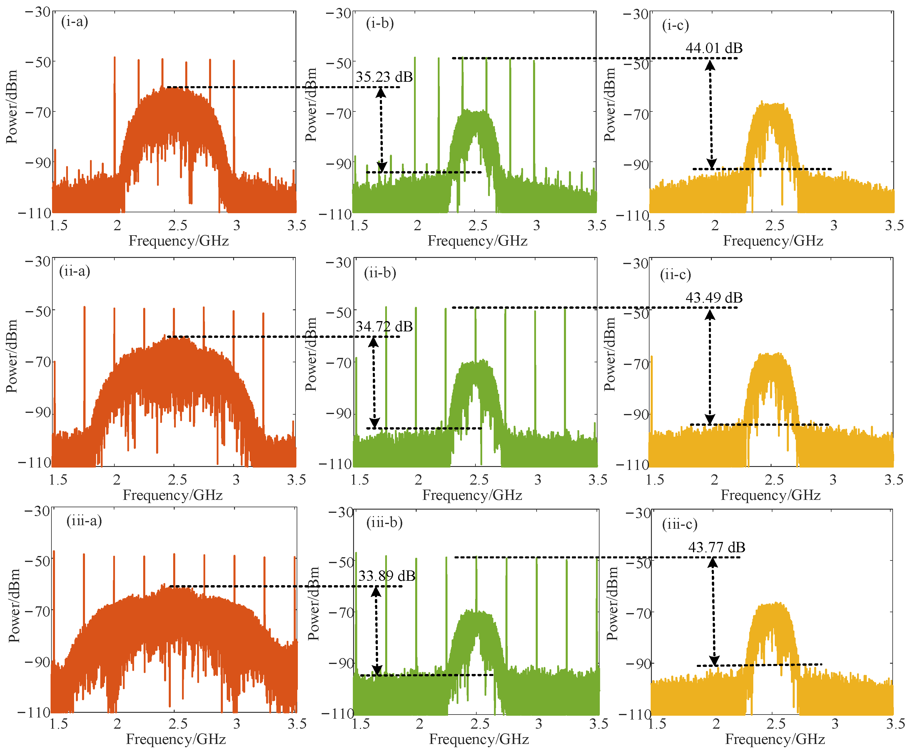
τREF are the amplitude, angular frequency and initial arrival time of the REF signal. As described above, the electrical signals of the four RF inputs are as follows. The spectrum diagrams of the input signals are shown in Figure 2a–c.
V x 1 ( t ) = V SOI sin ω SOI ( t + τ SOI ) + V SI sin ω SI ( t + τ SI ) + V image sin ω image ( t + τ image ) V x 2 ( t ) = V LO sin [ ω LO ( t + τ LO ) ] V y 1 ( t ) = V y 2 ( t ) = V REF sin ω REF ( t + τ REF )
By substituting Equation (5) into Equation (4) and using the modulation index βi to replace πVi/Vπ (i can be replaced by SOI, SI, image, LO and REF), the output of PDM-DPMZM can be written as:
E 1 ( t ) = { γ 2 E c exp ( j ω c t ) 10 ( I L / 20 ) { γ 1 γ exp j [ β SOI sin ω SOI ( t + τ SOI ) + β SI sin ω SI ( t + τ SI ) + β image sin ω image ( t + τ image ) ] + γ 1 ( 1 γ ) exp j φ x 1 exp j [ β SOI sin ω SOI ( t + τ SOI ) + β SI sin ω SI ( t + τ SI ) + β image sin ω i m a g e ( t + τ i m a g e ) ] + ( 1 γ 1 ) exp ( j φ x 3 ) { γ exp j β LO sin [ ω LO ( t + τ L O ) ] + ( 1 γ ) exp j φ x 2 exp j β L O sin [ ω L O ( t + τ L O ) ] } } e x ( 1 γ 2 ) E c exp ( j ω c t ) 10 ( I L / 20 ) { γ 1 γ exp [ j β REF sin ω R E F ( t + τ R E F ) ] + γ 1 ( 1 γ ) exp j φ y 1 exp [ j β R E F sin ω R E F ( t + τ R E F ) ] + ( 1 γ 1 ) exp ( j φ y 3 ) { γ exp [ j β R E F sin ω R E F ( t + τ R E F ) ] + ( 1 γ ) exp j φ y 2 exp [ j β R E F sin ω R E F ( t + τ R E F ) ] } } e y
The sub-modulators in both the upper and lower DPMZM all operate at the minimum transmission point (MITP) to suppress the optical carrier without loading information, thus increasing the power of modulated sidebands. Therefore, the phases introduced by the DC biases of the sub-modulators are all π. That is, φx1/2 and φy1/2 are π. φx3 and φy3 are the DC-induced phases of the main modulator of DPMZMx and DPMZMy. φx3 equals 0 to maximize the power of REF-modulated sidebands. By substituting the DC-bias-induced phase into Equation (6) and expanding Equation (6) based on the Bessel function to reserve the first-order sidebands for simplified analysis, Equation (6) is transferred into Equation (7). The Jacobi–Anger expansion (Bessel function) is an expansion of exponentials of trigonometric functions on the basis of their harmonics [18,19]. Here, it is also used to describe the spectral amplitudes of harmonics resulting from intensity modulation through electro-optic conversion. Jn(β) represents the nth-order Bessel function of the first kind. The spectrum diagrams of the modulated signals from DPMZMx and DPMZMy are shown in Figure 2d,e.
E 2 ( t ) = { E c exp ( j ω c t ) 10 ( I L / 20 ) γ 2 { γ 1 ( 2 γ 1 ) J 0 ( β S O I ) J 0 ( β S I ) J 0 ( β i m a g e ) + ( 1 γ 1 ) ( 2 γ 1 ) exp ( j φ x 3 ) J 0 ( β L O ) R e s i d u a l   o p t i c a l   c a r r i e r + 2 γ 1 J 1 ( β S O I ) J 0 ( β S I ) J 0 ( β i m a g e ) [ exp j ω S O I ( t + τ S O I ) exp j ω S O I ( t + τ S O I ) ] SOI - modulated   sidebands + 2 γ 1 J 1 ( β S I ) J 0 ( β S O I ) J 0 ( β i m a g e ) [ exp j ω S I ( t + τ S I ) exp j ω S I ( t + τ S I ) ] SI - modulated   sidebands + 2 γ 1 J 0 ( β S I ) J 0 ( β S O I ) J 1 ( β i m a g e ) [ exp j ω i m a g e ( t + τ i m a g e ) exp j ω i m a g e ( t + τ i m a g e ) ] Image - modulated   sidebands + 2 ( 1 γ 1 ) J 1 ( β L O ) exp ( j φ x 3 ) [ exp j ω L O ( t + τ L O ) exp j ω L O ( t + τ L O ) ] LO - modulated   sidebands } e x E c exp ( j ω c t ) 10 ( I L / 20 ) ( 1 γ 2 ) { ( 2 γ 1 ) J 0 ( β R E F ) Residual   optical   carrier + 4 J 1 ( β R E F ) [ exp j ω R E F ( t + τ R E F ) exp j ω R E F ( t + τ R E F ) ] REF - modulated   sidebands } e y
Then, the polarization orthogonal signals output by PDM-DPMZM will enter a polarization beam splitter (PBS) to be polarization-demultiplexed, and an optical time delay line (OTDL) will realize high-precision time delay tuning of the REF signal in the lower path. The polarization-demultiplexed signals will then enter the PBC for secondary polarization beam combination and be combined through an adjustable polarizer (Pol) with an angle, α. Therefore, the output signal of the Pol can be expressed as:
E 3 ( t ) = E c exp ( j ω c t ) 10 ( I L / 20 ) ( { cos α ( 2 γ 1 ) γ 2 [ γ 1 J 0 ( β S O I ) J 0 ( β S I ) J 0 ( β i m a g e ) + ( 1 γ 1 ) exp ( j φ x 3 ) J 0 ( β L O ) ] + sin α ( 2 γ 1 ) ( 1 γ 2 ) J 0 ( β R E F ) Residual   optical   carrier } + { 2 cos α γ 2 γ 1 J 1 ( β S O I ) J 0 ( β S I ) J 0 ( β i m a g e ) [ exp j ω S O I ( t + τ S O I ) exp j ω S O I ( t + τ S O I ) ] SOI - modulated   sidebands + 2 cos α γ 2 γ 1 J 0 ( β S I ) J 0 ( β S O I ) J 1 ( β i m a g e ) [ exp j ω i m a g e ( t + τ i m a g e ) exp j ω i m a g e ( t + τ i m a g e ) ] Image - modulated   sidebands + 2 cos α γ 2 ( 1 γ 1 ) J 1 ( β L O ) exp ( j φ x 3 ) [ exp j ω L O ( t + τ L O ) exp j ω L O ( t + τ L O ) ] LO - modulated   sidebands } + { 2 cos α γ 2 γ 1 J 1 ( β S I ) J 0 ( β S O I ) J 0 ( β i m a g e ) [ exp j ω S I ( t + τ S I ) exp j ω S I ( t + τ S I ) ] SI - modulated   sidebands + 4 sin α ( 1 γ 2 ) J 1 ( β R E F ) [ exp j ω R E F ( t + τ R E F + τ ) exp j ω R E F ( t + τ R E F + τ ) ] REF - modulated   sidebands } )
In Equation (8), the first brace is the residual optical carrier; the second brace contains SOI-, image-, and LO-modulated sidebands; and the third brace contains SI- and REF-modulated sidebands. Therefore, it can be seen from Equation (8) that the SIC conditions of amplitude matching and phase reversion can be achieved by adjusting the angle of Pol, and the time delay matching can be achieved by tuning the optical time delay line (OTDL). The manual OTDL commonly used at present is usually a passive device tuned by changing the length of the propagation path. The basic structure of an OTDL is packed with two fiber optic collimators and a reverse reflector on a movable platform [20]. The position of the movable reflector can be adjusted with some adjusting knobs so as to change the propagation path of the optical signal in the device and realize the adjustment of the time delay. Specifically, when the conditions shown in Equation (9) are satisfied, the SIC signal can be canceled directly in the optical domain.
cos α γ 2 γ 1 J 1 ( β S I ) J 0 ( β S O I ) J 0 ( β i m a g e ) = 2 sin α ( 1 γ 2 ) J 1 ( β R E F ) , τ S I = τ R E F + τ
The conditions for solving the parameters can be rewritten as:
tan α = γ 2 γ 1 J 1 ( β S I ) J 0 ( β S O I ) J 0 ( β i m a g e ) 2 ( 1 γ 2 ) J 1 ( β R E F ) ( α π 2 + n π ) , τ = τ S I τ R E F
As a result, through optical parameter regulation, the SI-modulated sidebands and REF-modulated sidebands in the third brace cancel each other out, leaving only the items in the first and second brace. A spectrum diagram output from the Pol is shown in Figure 2f. As can be seen from Figure 2f, after the adjustment of the Pol and optical time delay line, the REF-modulated sidebands (blue checked squares) and SI-modulated sidebands (solid green squares) are in reverse phase; then, amplitude and delay matching are satisfied, SI-modulated sidebands can be eliminated and, thus, SIC can be achieved directly. Replacing the residual carrier component with ξ (ξ = cosα(2γ−1) γ2[γ1J0(βSOI)J0(βSI) J0(βimage) + (1−γ1)exp(jφ3) J0(βLO)] + sinα(2γ−1)(1−γ2)J0(βREF)) to simplify the expression and substituting Equation (10) into Equation (8), the output can be obtained as:
E 3 ( t ) = E c exp ( j ω c t ) 10 ( I L / 20 ) ( ξ + 2 cos α γ 2 { γ 1 J 1 ( β S O I ) J 0 ( β SI ) J 0 ( β image ) [ exp j ω S O I ( t + τ S O I ) exp j ω S O I ( t + τ S O I ) ] SOI - modulated   sidebands + γ 1 J 0 ( β SI ) J 0 ( β SOI ) J 1 ( β image ) [ exp j ω i m a g e ( t + τ i m a g e ) exp j ω i m a g e ( t + τ i m a g e ) ] Image - modulated   sidebands + ( 1 γ 1 ) J 1 ( β LO ) exp ( j φ x 3 ) [ exp j ω L O ( t + τ L O ) exp j ω L O ( t + τ L O ) ] LO - modulated   sidebands } )
Then, the remaining signals are amplified by an erbium-doped fiber amplifier (EDFA) and injected into wavelength division multiplexing (WDM). Through WDM, the positively and negatively modulated sidebands of the SOI, image and LO signals are separated into two paths. Assuming that the passband responsiveness of WDM is ideal and the optical carrier falls on the edge of the passband response, the two signals output by WDM can be expressed as:
E u ( t ) = E c exp ( j ω c t ) 10 ( I L / 20 ) ( η 1 ξ + 2 cos α γ 2 { γ 1 J 1 ( β S O I ) J 0 ( β S I ) J 0 ( β i m a g e ) exp j ω SOI ( t + τ SOI ) + 1 st   SOI - modulated   sideband + γ 1 J 0 ( β SI ) J 0 ( β SOI ) J 1 ( β i m a g e ) exp j ω i m a g e ( t + τ i m a g e ) + 1 st   Image - modulated   sideband + ( 1 γ 1 ) J 1 ( β L O ) exp ( j φ x 3 ) exp j ω L O ( t + τ L O ) + 1 st   LO - modulated   sidebands } )
E d ( t ) = E c exp ( j ω c t ) 10 ( I L / 20 ) ( η 2 ξ 2 cos α γ 2 { γ 1 J 1 ( β S O I ) J 0 ( β S I ) J 0 ( β i m a g e ) exp j ω S O I ( t + τ S O I ) 1 st   SOI - modulated   sideband + γ 1 J 0 ( β S I ) J 0 ( β S O I ) J 1 ( β i m a g e ) exp j ω i m a g e ( t + τ i m a g e ) 1 st   I m a g e - modulated   sideband + ( 1 γ 1 ) J 1 ( β L O ) exp ( j φ x 3 ) exp j ω L O ( t + τ L O ) 1 st   LO - modulated   sideband } )
where η1 and η2 are the amplitude attenuation coefficients of the optical carrier in two paths after filtering by WDM. The process of going through WDM is shown in Figure 2g–i. The separated signals are converted into photocurrents by two photodetectors (PDs) with the same responsivity. The electrical signals obtained in the two paths are then combined in a 90-degree hybrid coupler (90°HC), the output of which can be expressed as:
i ( t ) = G R E c 2 10 ( I L / 10 ) ( η 1 2 | ξ | 2 + η 2 2 | ξ | 2 DC   c o m p o n e n t 4 ξ γ 1 γ 2 cos α J 1 ( β S O I ) J 0 ( β S I ) J 0 ( β i m a g e ) [ η 1 sin ω S O I ( t + τ S O I ) + η 2 cos ω S O I ( t + τ S O I ) ] SOI - l e a k a g e 4 ξ γ 1 γ 2 cos α J 0 ( β S I ) J 0 ( β S O I ) J 1 ( β i m a g e ) [ η 1 sin ω i m a g e ( t + τ i m a g e ) + η 2 cos ω i m a g e ( t + τ i m a g e ) ] Image - l e a k a g e 4 ξ γ 2 ( 1 γ 1 ) cos α J 1 ( β L O ) { η 1 sin [ ω L O ( t + τ L O ) + φ x 3 ] + η 2 cos [ ω L O ( t + τ L O ) φ x 3 ] } LO - l e a k a g e + 8 γ 1 ( 1 γ 1 ) γ 2 2 cos α 2 J 1 ( β S O I ) J 0 ( β S I ) J 0 ( β image ) J 1 ( β L O ) { cos [ ω S O I ( t + τ S O I ) ω L O ( t + τ L O ) φ x 3 + π 2 ] + cos [ ω S O I ( t + τ S O I ) ω L O ( t + τ L O ) + φ x 3 ] } SOI -   down - converted   signal + 8 γ 1 ( 1 γ 1 ) γ 2 2 cos α 2 J 1 ( β image ) J 0 ( β S O I ) J 0 ( β S I ) J 1 ( β L O ) { cos [ ω L O ( t + τ L O ) ω i m a g e ( t + τ i m a g e ) + φ x 3 + π 2 ] + cos [ ω L O ( t + τ L O ) ω i m a g e ( t + τ i m a g e ) φ x 3 ] } Image -   down - converted   signal )
Here, the gain of the EDFA is G, and the responsivity of the PDs is R. As can be seen from Equation (14), when the phase introduced by the DC bias of the main modulator in DPMZMx is 45 degrees, namely, φx3 equals π/4, the image interference can be canceled due to phase reversion and the desired IF signal is, thus, enhanced. Therefore, the useful IF signal, free of self-interference and image interference, can finally be obtained as Equation (15). The output of two PDs and the 90°HC is shown in Figure 2j–l.
i I F ( t ) = G R E c 2 10 ( I L / 10 ) ( ( η 1 2 + η 2 2 ) | ξ | 2 DC   component 4 ξ γ 1 γ 2 cos α J 1 ( β S O I ) J 0 ( β S I ) J 0 ( β image ) [ η 1 sin ω S O I ( t + τ S O I ) + η 2 cos ω S O I ( t + τ S O I ) ] SOI - l e a k a g e 4 ξ γ 1 γ 2 cos α J 0 ( β S I ) J 0 ( β S O I ) J 1 ( β image ) [ η 1 sin ω i m a g e ( t + τ i m a g e ) + η 2 cos ω i m a g e ( t + τ i m a g e ) ] Image - l e a k a g e 4 ξ γ 2 ( 1 γ 1 ) cos α J 1 ( β L O ) { η 1 sin [ ω L O ( t + τ L O ) + π 4 ] + η 2 cos [ ω L O ( t + τ L O ) π 4 ] } LO - l e a k a g e + 16 γ 1 ( 1 γ 1 ) γ 2 2 cos α 2 J 1 ( β S O I ) J 0 ( β S I ) J 0 ( β image ) J 1 ( β L O ) cos [ ω S O I ( t + τ S O I ) ω L O ( t + τ L O ) + π 4 ] SOI -   down - converted   signal )
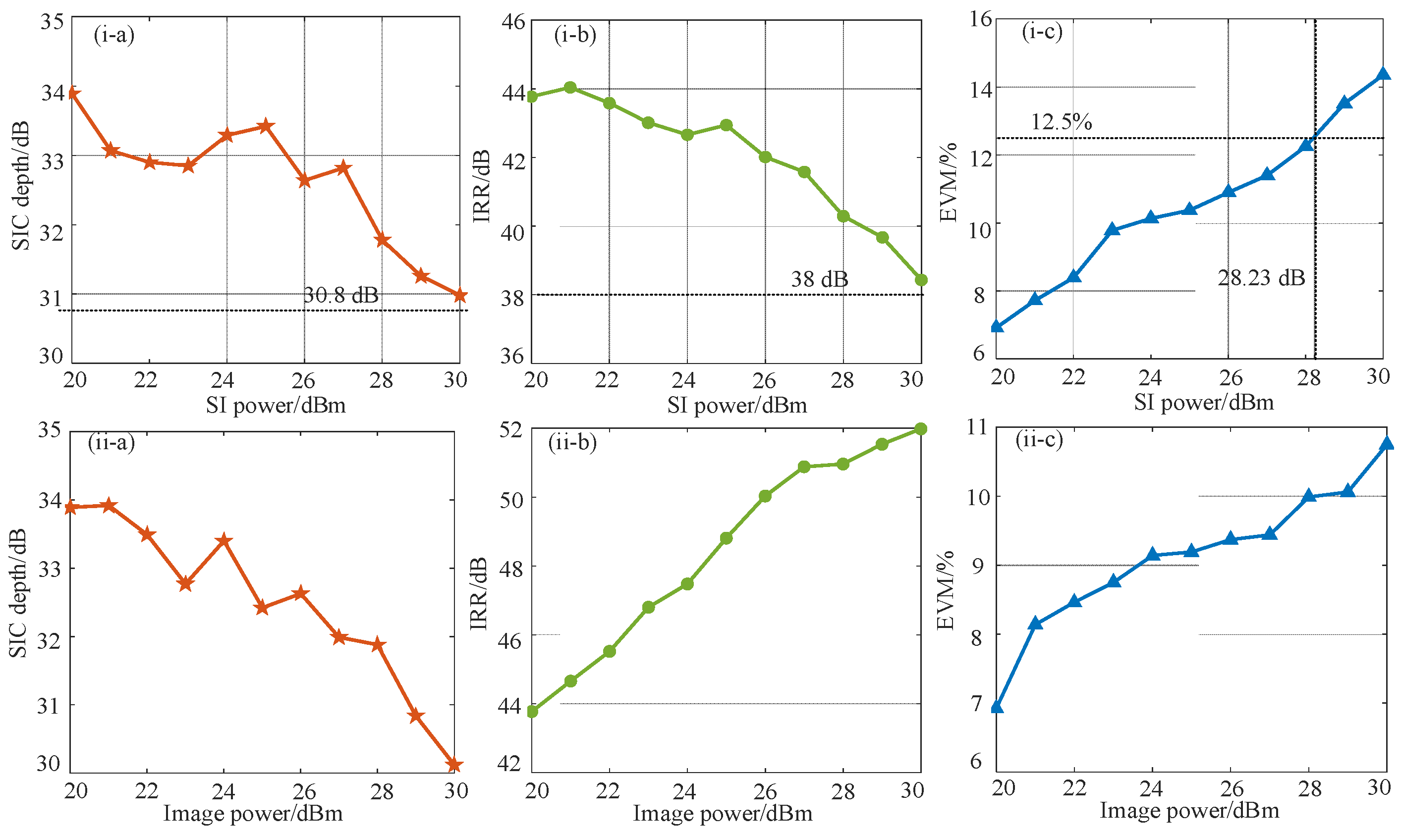
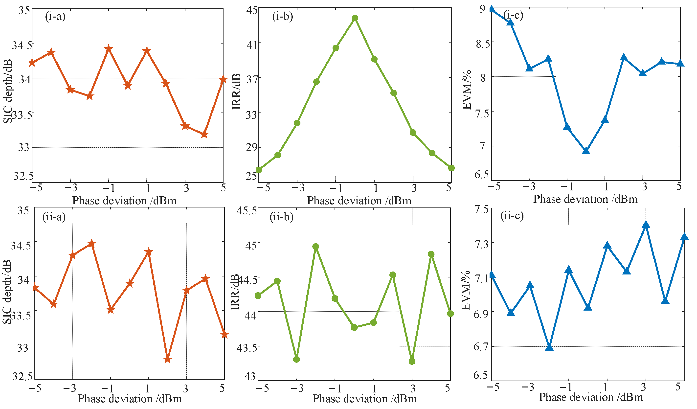
As can be seen from Equation (15), image rejection is performed. However, the non-ideal ER results in the higher power of the residual carrier, which finally leads to a high-power DC component and the leakage of RF and LO signals. Fortunately, the deterioration of ER has no effect on the SIC and IRM performances. The stray component can be filtered by the straighter and the electric filter. The deterioration of ER may cause changes in the spectral ratio, resulting in a change in useful signal power, but the change is within the acceptable range, which can be compensated for by an amplifier. Therefore, the scheme has good resistance to ER deterioration. In addition, MZMs with extremely high ER have been verified, which provides the possibility for further improving system performance [21].
In addition, the operating bandwidth of the modulator may affect the signal-tuning frequency range. However, most of the current commercially available modulators have bandwidths above 23 GHz to meet the needs of general systems [22]. With further improvement in manufacturing technology, the bandwidth of modulators is gradually improving [23]. Superior performance modulators will help further extend the system bandwidth.
The conversion gain of the receiver, defined as the power ratio between the IF and RF signals, can reflect the loss and efficiency of the whole system to some extent, which can be calculated as [24]:
G a i n ( dB ) = 10 log ( P IF P RF ) = 10 log { [ 16 π G R E c 2 γ 1 ( 1 γ 1 ) γ 2 2 cos α 2 J 0 ( β SI ) J 0 ( β image ) J 1 ( β LO ) 10 ( I L / 10 ) V π ] 2 R out R in }
where PIF and PRF are the powers of the IF and RF signals. Rout and Rin are the output- and input-matched impedance of the system. In principle, the conversion gain can be improved by applying PD with higher responsivity and a modulator with smaller half-wave voltage, as well as by increasing the gain of the amplifier, improving the optical carrier intensity of the laser output or setting the proper modulation index of the LO signal.

3. Simulation and Discussion

A simulation based on the setup shown in Figure 1 was carried out to verify the feasibility of the proposed scheme by using the commercial software “Optisystem” (Ottawa, ON, Canada). An optical carrier centered at 193.1 THz was generated from an LD with a power of 16 dBm. After being adjusted by the following PC, the optical carrier was injected into the modulator. The half-wave voltage, extinction ratio and insertion loss were set as the typical values of 3.5 V, 20 dB and 5 dB. The generated SOI, SI and image signals were first combined and then sent to one RF input port of the DPMZMx; meanwhile, a sinusoidal signal was applied to another RF input port of the DPMZMx as the LO signal. The REF signal was first divided into two paths equally and injected into two RF ports of DPMZMy. Carrier-suppressed double-sideband (CS-DSB) signals were generated by making the sub-modulators operate at the MITP, and the REF-modulated signal power was guaranteed to be maximum by making the main modulator of DPMZMy operate at the MATP. The center frequencies of the two channels in the WDM were set as 193.085 THz and 193.115 THz, and the channel bandwidth was set as 28 GHz. The gain of EDFA was set as 2 dB, and the responsivity of PD was set as 0.95 A/W. The parameters were set according to the default values of “Optisystem” or commonly used device models [25,26].

3.1. Performance of Wideband SIC and IR

First, the wideband SIC and IR performances were demonstrated. The LO signal was a single-tone sinusoidal signal with a power of 20 dBm. The SOI signal was a 500 MHz wideband 16-quadrature amplitude modulation (QAM)-modulated signal with a power of 10 dBm. The image, SI and REF signals were also 16-QAM-modulated signals with powers of 20 dBm. First, the wideband SIC performance of the IRM was verified, making the image signal disconnected. The SOI, SI and REF signals were centered at 12.5 GHz, making the down-conversion IF signal centered at 2.5 GHz. The simulation results of the SIC performance with the bandwidth of the SI signal switched to 1 GHz, 1.5 GHz and 2 GHz are shown in Figure 3.
As can be seen from the figure, the low-power SOI was buried under the strong SI signal when the SIC was disabled. After the SIC function was enabled, a cancellation depth higher than 38 dB was achieved, and the wideband SI signals with bandwidths of 1 GHz, 1.5 GHz and 2 GHz were all canceled to the noise floor. This means that wideband, deep SIC can be achieved through the IRM structure.
Next, in order to verify its IR function, we disconnected the SI and REF signals and input the image signal, the center frequency of which is symmetric with the SOI frequency in relation to the LO signal. That is, the image signal was centered at 7.5 GHz. The IR performances of different bandwidths are shown in Figure 4. As can be seen from the figure, for the image signals with bandwidths of 1, 1.5 and 2 GHz, when the phase shift φbiasx3 induced by the Vbiasx3 is initially 0, the image signal cannot be suppressed, making the SOI buried under the image interference. When φbiasx3 turns to π/4, that is, a pair of orthogonal LO signals are generated, the image interference is eliminated, making the electrical spectrum of SOI obviously visible. For image signals with different bandwidths, the IRM can guarantee an image rejection ratio (IRR) over 35 dB, indicating that it has good wideband deep image rejection capability.
Then, the frequencies of the SOI (the same frequency as the SI and REF signals), image and LO signals were tuned to verify the frequency tunability of the demonstrated SIC and IR functions. The SOI switched from 6.5 GHz to 28.5 GHz with a step of 2 GHz, which means that the signal frequency was covered from the C band to Ka band. The LO signal switched from 4 GHz to 26 GHz correspondingly to make the IF signal fixed at 2.5 GHz. The corresponding image signal frequencies were from 1.5 GHz to 23.5 GHz. The power of the signals is consistent with the above analysis. Taking the interference signal with a 2 GHz bandwidth as an example, the SIC and IR performances at different frequency bands were explored. By disconnecting the image signal, the SIC function was performed, and the curve of SIC depth versus SOI frequency is shown in Figure 5a. Similarly, by disconnecting the SI and REF signals, the IR function was verified, and the curve of IRR versus SOI frequency is shown in Figure 5b. As can be seen from the figure, from the C band to Ka band, the SIC depth and IRR are over 38 dB and 35 dB, respectively, indicating that the scheme has good frequency tunability.

3.2. Simultaneous SIC and IR with Recovery of SOI

Then, the performance of simultaneous SIC and IR with the recovery of SOI was investigated. In order to facilitate observation, the SI signal was set to a 16 QAM signal with different bandwidths and a power of 20 dBm, while the image interference was set to multiple single-tone signals covering different frequency bands with a power of 20 dBm. The parameters of SOI and LO signals remained unchanged. The bandwidths of the SI signal were set as 1 GHz, 1.5 GHz and 2 GHz. Correspondingly, the coverage of the multitone image signal was also set as 1 GHz, 1.5 GHz and 2 GHz. When all signals were injected into the system, the reference branch was first disconnected, and the DC-bias-induced phase φbiasx3 was set to 0 so that the SIC and IR functions were disabled. The electrical spectra are shown in Figure 6a, wherein the SOI is completely invisible. At this time, the recovered constellation diagrams of desired IF signals are shown in Figure 7a, which is relatively messy. The error vector magnitudes (EVMs) were calculated as 24.06%, 28.98% and 28.04% in these three conditions through offline digital signal processing (DSP) including normalization, equalization and EVM calculation. When the reference branch was connected to realize SIC, the SI was effectively eliminated with an SIC depth over 33 dB, while the image signal was still observed in the spectra and would interfere with the recovery of the desired signal. When the DC bias φbiasx3 was set to 45 degrees, the image-converted signal was also eliminated with an IRR over 43 dB, leaving only the useful signal clearly visible in the spectra, and clear constellation diagrams are shown in Figure 7b with the EVMs reduced to 7.15%, 6.74% and 6.92%. This indicates that satisfactory performances of in-band interference cancellation and signal recovery were achieved.

3.3. Interference Cancellation and Signal Recovery Performance under Strong Interference

The main purpose of suppressing strong interference is to effectively recover weak signals. Therefore, the interference cancellation performance of the system and the recovery performance of useful signals with two kinds of high-power in-band interference signals were investigated. As shown in Figure 8, we plotted the SIC depth, IRR and EVM of useful signal recovery with the power of the self-interference signal and image interference rise to reflect the system performance under high-power interference signals. The wideband SI signal of 2 GHz bandwidth and the multi-carrier image signal with the frequency coverage of 2 GHz bandwidth were selected with the frequency centered at 12.5 GHz. The parameters of SOI remained unchanged. First, the power of the image signal remained at 20 dBm, and the SI signal power changed from 20 dBm to 30 dBm. The measured SIC depth, IRR and calculated EVM are shown in Figure 8i.
It can be seen from the figure that, with the increase in the SI signal power, the performance of SIC and IR, as well as the quality of signal recovery, all show a declining trend. Fortunately, the SIC depth is above 30.8 dB, and the IRR is above 38 dB. Furthermore, the calculated EVMs can still meet the requirements of the 3GPP limit for 16-QAM-modulated signals when the SI power does not exceed 28.23 dB. Similarly, we set the SI signal power to 20 dBm and changed the power of the image signal from 20 dBm to 30 dBm. As can be seen from Figure 8ii, when the image signal power rises, the SIC depth deteriorates gradually, while it is always higher than 30 dB. The IRR rises with the increase in the image signal power. The EVM deteriorates gradually, but it is always lower than 11%, satisfying the 3GPP limit requirements for 16-QAM-modulated signals. Therefore, in general, this scheme can deeply eliminate in-band interference and effectively recover weak signals in the presence of high-power interference.

3.4. Ability to Cope with Phase Imbalance of Electrical IF 90-Degree HC

The electrical IF 90-degree HC is a key device for image rejection schemes using the Hartley-structure-based phase cancellation method. However, there may exist an inherent phase imbalance between the two paths, making the phase difference of the two signals output by the phase-related device deviate from 90 degrees, thus affecting the image rejection performance. Therefore, it is necessary to explore the influence of this non-ideal factor on system performance. We set the phase deviation in the electrical IF 90-degree HC in the range of −5 degrees ~5 degrees, and the measured SIC depth, IRR and EVM without any compensation measures are shown in Figure 9i.
As can be seen from the figure, when the phase difference between the two paths gradually deviates from the ideal value, the IRR deteriorates sharply. Since the SI was canceled in the optical domain, the SIC performance was basically not affected. In addition, the EVM also showed a worsening trend with the increase in phase deviation. However, since the image interference was a multi-carrier single-frequency signal, the EVM deterioration was not serious. If the image interference is a wideband-modulated signal, the deterioration of recovery performance will be much more serious. Therefore, the impact of phase deviation cannot be ignored. Fortunately, it can be seen from Equation (5) that, when phase deviation occurs, it can be compensated for by adjusting the phase introduced by the DC bias, and the obtained results are shown in Figure 9ii. It can be seen that there was no obvious deterioration of SIC depth, IRR and EVM, which fluctuated within 2 dB, 2 dB and 1%, respectively. Therefore, this scheme can effectively deal with the deterioration of performance caused by the phase imbalance of the electrical IF 90-degree HC by adjusting the phase introduced by DC bias.

3.5. The Effect of Pol Tuning Accuracy

In order to further explain the influence of Pol tuning accuracy on SIC performance, we explored it through simulation. The tunable polarizer can realize 360-degree rotation by using a graduated hand wheel [27]. Generally, the resolution of a commercially tunable Pol is 1 degree, while, in fact, the rotation angle is continuously adjustable, and in theory, any value can be achieved by turning the graduated hand wheel. In the analysis, the angle of the Pol was offset from the ideal value between −1 degree and 1 degree, tuned in steps of 0.1 degrees. The curve of the SIC depth and offset value of Pol angle was obtained, as shown in the blue line in Figure 10. As can be seen from the figure, with the increase in the offset value, the SIC depth decreases gradually. When the offset value is 1 degree, the SIC depth deteriorates by about 10 dB, but it remains above 29 dB, in general.
In order to compare with the schemes cited in this manuscript (Refs. [12,13]) using an electric attenuator to achieve amplitude matching, the influence of the electric attenuator tuning accuracy on the performance of SIC performance was also carried out through simulation. Currently, for commonly used commercially available wideband electrical attenuators (DC-18 GHz), the tuning step of the electrical attenuators is 1 dB, and continuous tuning is usually possible [28]. Therefore, an electric attenuator was used to adjust the power of the reference branch in the simulation so that the power of the reference branch was offset from the matched ideal value with a scale of −1 dB to 1 dB and a step of 0.1 dB. The curve of the reference branch power offset value and SIC depth is shown as a red line in Figure 10. As can be seen from the figure, as the reference branch power offset increases, the SIC depth decreases gradually. When the offset value is 1 dB, the SIC depth deteriorates by over 16 dB. It can be seen from the two curves that the deterioration of SIC depth due to power mismatch caused by the electric attenuator is more obvious and serious. Therefore, Pol tuning for SIC operation has better resistance to tuning imprecision.

4. Conclusions

A photonic-enabled IRM for ultrawideband SIC and simultaneous high-speed SOI recovery was proposed. The scheme was constructed based on a single electro-optic modulator in a coherent optical system, bringing it the advantages of compact structure and low system complexity. By virtue of optical polarization regulation and optical high-precision time delay matching, the SI signal could be canceled directly in the optical domain with a large depth and wide bandwidth. A pair of orthogonal LO signals were constructed by virtue of the phase shift introduced by DC bias to realize the IR function based on the Hatley structure, avoiding the high-frequency electrical 90-degree HC required to generate orthogonal LO or RF signals in the electrical domain, thus ensuring broadband and deep IR operation. The simulation results showed that the 2 GHz wideband SI and image interference could be suppressed over 38 dB and 35 dB in a large frequency coverage. When there are both wideband SI and wideband multi-carrier single-frequency image interference, it can effectively solve the problem of in-band interference in RF transceivers, which guarantees signal recovery performance. It was also verified that the proposed scheme could resist high-power interference and cope with the phase imbalance of phase-related devices. This contributed to effective signal recovery under strong interference to provide full play to the advantages of photonic-enabled IBFD RF systems and promotes their practical application prospects.

Author Contributions

Conceptualization, H.L.; methodology, H.L.; software, C.G. and G.W.; validation, X.L.; formal analysis, T.Z.; resources, Q.M.; data curation, Y.Z.; writing—original draft preparation, H.L.; writing—review and editing, Z.Z. and S.Z.; visualization, H.L.; supervision, T.Z. and S.Z.; project administration, Z.Z. and S.Z.; funding acquisition, Z.Z., T.Z. and S.Z. All authors have read and agreed to the published version of the manuscript.

Funding

This research was funded by the National Natural Science Foundation of China (No.: 61571461 and 61401502), the National Postdoctoral Program for Innovative Talents (No.: BX201700056), the Project “science and technology new star of Shaanxi province” (No.: 2019KJXX-082), and The Youth Innovation Team of Shaanxi Universities (No.: 2022-106).

Institutional Review Board Statement

Not applicable.

Informed Consent Statement

Not applicable.

Data Availability Statement

Not applicable.

Conflicts of Interest

The authors declare no conflict of interest.

References

  1. Pan, S.L.; Zhu, D. Broadband cognitive radio enabled by photonics. In Proceedings of the 45th European Conference on Optical Communication, Dublin, Ireland, 22–26 September 2019. [Google Scholar]
  2. Minasian, R.A. Ultra-Wideband and Adaptive Photonic Signal Processing of Microwave Signals. IEEE J. Quantum Elect. 2016, 52, 1–13. [Google Scholar] [CrossRef]
  3. Clark, T.R.; Waterhouse, R. Photonics for RF Front Ends. IEEE Microw. Mag. 2011, 12, 87–95. [Google Scholar] [CrossRef]
  4. Capmany, J.; Li, G.F.; Lim, C.; Yao, J.P. Microwave Photonics: Current challenges towards widespread application. Opt. Express 2013, 21, 22862–22867. [Google Scholar] [CrossRef] [PubMed]
  5. Cabon, B. Microwave Photonics Mixing. Sci. Iran. 2010, 17, 149–162. [Google Scholar]
  6. Tang, Z.Z.; Li, Y.F.; Yao, J.P.; Pan, S.L. Photonics-Based Microwave Frequency Mixing: Methodology and Applications. Laser Photonics Rev. 2019, 14, 1800350. [Google Scholar] [CrossRef]
  7. Zhang, L.; Ansari, N. A framework for 5 G networks with in-band full-duplex enabled drone-mounted base-stations. IEEE Wirel. Comm. 2019, 26, 121–127. [Google Scholar] [CrossRef]
  8. Kolodziej, K.E.; Perry, B.T.; Herd, J.S. In-band full-duplex technology: Techniques and systems survey. IEEE Trans. Microw. Theory Techn. 2019, 67, 3025–3041. [Google Scholar] [CrossRef]
  9. Adles, E.J.; Clark, T.R.; Dennis, M.L.; Karim, A.M.; McKenna, T.P. Interferer cancellation in coherent optical RF receivers via optical phase modulation. In Proceedings of the IEEE Photonics Conference 2012, Burlingame, CA, USA, 23–27 September 2012. [Google Scholar]
  10. Zhu, D.; Pan, S.L. Photonics-Based Microwave Image-Reject Mixer. Photonics 2018, 5, 6. [Google Scholar] [CrossRef] [Green Version]
  11. Urick, V.J.; Godinez, M.E.; Mikeska, D.C. Photonic Assisted Radio-Frequency Interference Mitigation. IEEE J. Lightw. Technol. 2020, 38, 1268–1274. [Google Scholar] [CrossRef]
  12. Weng, B.Y.; Chen, Y.; Chen, Y. Photonic-assisted wideband frequency downconverter with self-interference cancellation and image rejection. Appl. Optics 2019, 58, 3539–3547. [Google Scholar] [CrossRef] [PubMed]
  13. Yang, D.C.; Wu, F.Z.; Yang, F.; Yin, J.; Wang, D.Y.; Wang, Y.X.; Li, T.; Zhou, T. Photonic-Assisted Reconfigurable LO Harmonic Downconverter with RF Self-Interference Cancellation and Image-Rejection. IEEE J. Lightw. Technol. 2023, 41, 149–158. [Google Scholar] [CrossRef]
  14. Zhu, D.; Hu, X.P.; Chen, W.J.; Ben, D.; Pan, S.L. Photonics-enabled simultaneous self-interference cancellation and image-reject mixing. Opti. Lett. 2019, 44, 5541–5544. [Google Scholar] [CrossRef] [PubMed]
  15. Zhu, Z.H.; Gao, C.R.; Zhao, S.H.; Zhou, T.; Li, H.; Meng, Q.Q.; Tan, Q.G. Filter-Less Photonic RF Image-Reject Mixing With Simultaneous Self-Interference Cancellation and Fiber Transmission. IEEE J. Lightw. Technol. 2022, 40, 7799–7807. [Google Scholar] [CrossRef]
  16. Yu, Y.H.; Zhang, Y.H.; Huang, L.; Xiao, S.L. Performance analysis of an optical self-interference cancellation system with a directly modulated laser-based demonstration. Appl. Optics 2018, 57, 1284–1291. [Google Scholar] [CrossRef] [PubMed]
  17. Zhang, Y.H. Key Techniques of Broadband Adaptive Optics Self—Interference Cancellation in In-band Full-Duplex Communication. Ph.D. Thesis, Shanghai Jiao Tong University, Shanghai, China, December 2018. [Google Scholar]
  18. Abramowitz, M.; Stegun, I. Handbook of Mathematical Functions with Formulas, Graphs, and Mathematical Tables; Dover Publications: New York, NY, USA, 1965. [Google Scholar]
  19. Colton, D.; Kress, R. Inverse Acoustic and Electromagnetic Scattering Theory Applied Mathematical Sciences; Springer: New York, NY, USA, 1998. [Google Scholar]
  20. Optical Delay Lines. Available online: https://www.oe1.com/encyclopedia/7060504902507196416.html (accessed on 15 May 2023).
  21. Brunetti, G.; Sasanelli, N.; Armenise, M.N.; Ciminelli, C. High performance and tunable optical pump-rejection filter for quantum photonic systems. Opt. Laser Technol. 2021, 139, 106978. [Google Scholar] [CrossRef]
  22. Yen, H. Optical technology for microwave applications. In Proceedings of the IEEE MTT-S International Microwave Symposium, St. Louis, MO, USA, 4–6 June 1985. [Google Scholar]
  23. 40 GHz Bandwidth Sumitomo IQ Modulator Lithium Niobate Fiber Modulator T.SBXH1.5-XX Series. Available online: http://www.realphoton.com/archives/2955 (accessed on 16 May 2023).
  24. Sotom, M.; Benazet, B.; Kernec, A.L.; Michel, M. Microwave photonic technologies for flexible satellites telecom payloads. In Proceedings of the 35th European Conference on Optical Communication, Vienna, Austria, 20–24 September 2009. [Google Scholar]
  25. Fujitsu DP-IQ Modulator Lithium Niobate Fiber Modulator FTM7977HQA. Available online: http://www.realphoton.com/archives/1270 (accessed on 18 May 2023).
  26. OptiSystem Overview. Available online: https://optiwave.com/optisystem-overview/ (accessed on 13 May 2023).
  27. JW1511 Mechanical Adjustable Polarizer. Available online: https://www.joinwit.com/products-info.html?product_id=553 (accessed on 16 May 2023).
  28. TELLE Adjustable Electrical Attenuator. Available online: http://www.rebes.net/product-show.php?id=301 (accessed on 16 May 2023).
Figure 1. Schematic diagram of the proposed IRM with simultaneous SIC. LD: laser diode; PC: polarization controller; PDM-DPMZM: polarization-division-multiplexing dual-parallel Mach–Zehnder modulator; DPMZM: dual-parallel Mach–Zehnder modulator; MZM: Mach–Zehnder modulator; 90°PR: 90-degree polarization rotator; PBC: polarization beam combiner; PBS: polarization beam splitter; OTDL: optical time delay line; Pol: polarizer; EDFA: erbium-doped fiber amplifier; WDM: wavelength division multiplexing; PD: photodetector; 90°HC: 90-degree hybrid coupler. Label (a) represents the impaired signals containing SOI, SI and image signals are injected into the system, label (b) represents the LO signal is injected into the system, label (c) represents the REF signal is injected into the system. Label (d,e) represents the modulated signals have reached the output end of the upper and lower sub-modulators, respectively, label (f,g) represents the modulated signals have reached the output end of the Pol and EDFA, respectively. Label (h,i) represents the amplified signals have reached the output end of the upper and lower channels of WDM after demultiplexing. Label (j,k) represents the demultiplexed signals are photodetected and output by the upper and lower channels of corresponding PDs. Label (l) represents the combined signal have reached the output end of HC.
Photonics 10 00657 g001
Figure 2. Schematic spectrum diagrams of different points. (a) RF input of MZMx1, (b) RF input of MZMx2, (c) RF input of DPMZMy, (d) optical output of DPMZMx, (e) optical output of DPMZMy, (f) optical output of WDM, (g) optical output before WDM, (h) one output of WDM, (i) another output of WDM, (j) electrical output of upper PD, (k) electrical output of lower PD, (l) electrical output of the 90°HC. The red arrows in insets (f,g,l) indicate the evolution of the signal before and after SIC parameters tuning, WDM demultiplexing, and HC coupling.
Photonics 10 00657 g002
Figure 3. Electrical spectra of the down-converted IF signals and self-interference with (yellow line) and without SIC (orange line) with the bandwidths of SI set as (a) 1 GHz, (b) 1.5 GHz and (c) 2 GHz.
Photonics 10 00657 g003
Figure 4. Electrical spectra of the down-converted IF signals and image interference with (yellow line) and without IR (green line) with the bandwidths of image signal set as (a) 1 GHz, (b) 1.5 GHz and (c) 2 GHz.
Photonics 10 00657 g004
Figure 5. Measure curves of (a) SIC depth and (b) IRR versus SOI frequency with SIC or IR function enabled.
Photonics 10 00657 g005
Figure 6. Measured output electrical spectra (a) with SIC and IR functions disabled, (b) with SIC function enabled and IR function disabled, (c) with SIC and IR functions enabled. The bandwidths of SI signal and frequency coverage of the multitone image signal were set as (i) 1 GHz, (ii) 1.5 GHz and (iii) 2 GHz.
Photonics 10 00657 g006
Figure 7. The SOI recovery performance with SIC and IR functions both (a) disabled or (b) enabled. The bandwidths of SI signal and frequency coverage of the multitone image signal were set as (i) 1 GHz, (ii) 1.5 GHz and (iii) 2 GHz.
Photonics 10 00657 g007
Figure 8. Measurement curves of (a) SIC depth, (b) IRR and (c) EVM of received IF signal versus (i) SI and (ii) image signal power with SIC and IR functions enabled.
Photonics 10 00657 g008
Figure 9. Measurement curves of (a) SIC depth, (b) IRR and (c) EVM of received IF signal versus phase deviation in electrical IF 90-degree HC with (i) DC bias not adjusted, (ii) DC bias adjusted.
Photonics 10 00657 g009
Figure 10. The relationship of SIC depth with offset value of reference branch power and offset value of polarizer angle.
Photonics 10 00657 g010
Disclaimer/Publisher’s Note: The statements, opinions and data contained in all publications are solely those of the individual author(s) and contributor(s) and not of MDPI and/or the editor(s). MDPI and/or the editor(s) disclaim responsibility for any injury to people or property resulting from any ideas, methods, instructions or products referred to in the content.

