Article

Modeling Lattice Matched Dilute Nitride Triple and Quadruple Junction Solar Cells on Virtual SiGe Substrate

Department of Electrical Electronics Engineering, Faculty of Engineering, Gazi University, 06570 Ankara, Turkey
Photonics 2023, 10(6), 630; https://doi.org/10.3390/photonics10060630
Submission received: 8 March 2023 / Revised: 6 May 2023 / Accepted: 25 May 2023 / Published: 30 May 2023
(This article belongs to the Topic Photovoltaic Materials and Devices)

Abstract

:
A lattice matched triple junction solar cell (TJSC) structure with a GaAs0.58 P0.42 top cell and bandgap tunable GaNxAs1-x-zPz middle and bottom cells on virtual SiGe substrate is proposed in this study. SiGe/Si substrate is preferred as it is a low-cost substrate and because it provides a lattice constant at which bandgap tunable dilute nitride materials that are appropriate for highly efficient multijunction solar cells can be obtained. By changing the nitrogen content in GaNxAs1-x-zPz, the bandgap of the middle and bottom subcells is adjusted to the optimum values. The bandgap of the top cell is constant at 1.95 eV. Three models with different values of surface recombination velocities and Shockley–Read–Hall recombination lifetimes are applied to the presented TJSC structure. Peak efficiencies of 48.9%, 40.6% and 33.7% are achieved at EG2 = 1.45 eV and EG3 = 1.04 eV for Model 1, EG2 = 1.45 eV and EG3 = 1.15 eV for Model 2, and EG2 = 1.5 eV and EG3 = 1.17 eV for Model 3, respectively. A fourth bandgap adjustable GaNxAs1-x-zPz junction is inserted into the system and a significant improvement is obtained under high sun concentration for Models 1 and 2. The presented original results are very promising because the variable bandgaps provide very efficient absorption of incoming spectrum.

1. Introduction

The most common solar cells used in space and concentrated photovoltaic systems (CPV) are multijunction solar cells (MJSC) based on III–V semiconductors, which achieve the highest efficiency of 39.2% under 1 sun illumination of AM 1.5 spectrum and 47.6% under 665 suns [1].
In CPV applications, even a small increment in efficiency provides a significant improvement in performance of the system. Therefore, novel materials and structure designs are being investigated to increase the efficiency of MJSC for which GaAs, Ge and InP are mostly preferred as the substrate material.
Despite the high efficiencies provided by multijunction solar cells, their use in terrestrial applications is limited due to the high cost of raw materials and their production. In silicon-based conventional solar cells, which dominate the solar cell market in terrestrial applications [2], a maximum efficiency of 26.6% [3] is provided which is close to the detailed balance limit efficiency [4]. In order to obtain higher efficiency than conventional Si solar cells and to reduce the cost of multijunction cells, studies have focused on structures in which III-V semiconductors are grown on Si substrate [5].
The use of silicon with III-V semiconductors causes problems in practice due to a large thermal expansion difference and lattice mismatch. Mechanical stacking and wafer bonding approaches have been used to overcome this problem. These approaches have achieved extremely high efficiencies [6] but suffer from high costs as they require two substrates. The second approach in this regard is monolithic structures where junction materials are grown heteroepitaxially on a single substrate. To avoid the negative effects of large lattice mismatch and thermal expansion difference between III-V semiconductors and Si, a Ge/Si buffer layer is inserted between them. This application has provided successful results in LEDs [7], lasers [8], photodiodes [9] and bipolar transistors [10]. Single junction GaAs [11] and InGaP [12] solar cells grown on SiGe/Si virtual substrates have been investigated and promising results were obtained. GaInP/GaAs tandem [13] and GaInP/GaInAs/Ge triple junction [14] solar cells on virtual Ge/Si substrate and GaAsP/SiGe dual junction [15,16,17] solar cell structures have also been presented.
Dilute nitrides refer to compound semiconductors that include small amounts of nitrogen. Typically, when an order of a few atomic percent of nitrogen is added to compound semiconductors such as GaAs, GaP, InP, and several others, both their bandgaps and lattice constants change. Hence, bandgap tunable lattice matched materials which are potentially good candidates for use in high efficiency solar cells are obtained [18]. GaInNAsSb and InGaAsN are the most commonly proposed subcell materials for Ge- and GaAs-based lattice matched MJSC designs [19,20,21,22,23,24,25,26]. In [19], Aho et al. modeled a four junction solar cell including two GaInNAsSb bottom junctions with bandgap of 0.9 and 1.2 eV and fabricated an AlGaAs/GaAs/GaInNAsSb/GaInNAsSb solar cell structure on GaAs substrate. The obtained efficiency was 25% under AM1.5 illumination, whereas the theoretically expected efficiency was 34.7%. A wide bandgap AlGaInP material was added as the top junction and a five junction solar cell that widely covered the spectrum was obtained in [20]. In [21], over 50% efficiency under 1000 suns was estimated for a six junction solar cell with GaInNAsSb bottom cells. A GaInP/GaAs/InGaAsN TJSC with 30.2% efficiency under AM0 illumination was demonstrated in [22]. Degradation and defect properties of InGaAsN subcells are presented in [23,24]. An As-grown InGaAsN subcell was analyzed in [25] and a significant improvement was obtained.
Si lattice matched dilute nitride materials have also been investigated in recent studies. GaN0.02P0.98 with a bandgap of 1.94 eV that is lattice matched to Si is proposed as top cell material in [26]. GaNAsP is suggested as a photovoltaic material for multijunction solar cells in [27]. Zang et al. presented a theoretical model for a Si-based lattice matched TJSC. GaNP lattice matched with Si was used as the top cell, bandgap tunable GaNAsP as the middle cell, and Si as the bottom cell material. They used three different parameter models for surface recombination rates and carrier lifetimes and the highest efficiency obtained was 43.74% at AM1.5 illumination when the bandgap of GaNAsP was 1.483 eV. The adjustable bandgaps obtained by III-V-N materials in MJSC provide absorption of the larger part of the sun spectrum that improves efficiency. To absorb wider bands, ultra-thin structures are also proposed [28,29,30].
The bandgap of Si lattice matched GaAsNP can be at least 1.4 eV even when the nitride content is increased to 7%. This study aims to use bandgap adjustable GaAsNP for second, third and fourth junctions of MJSC which means a bandgap variation between 0.8 eV and 1.6 eV is needed for optimum bandgap combination. To achieve this, a SiGe virtual substrate with a lattice constant of 5.568 A was chosen instead of Si substrate and the lattice constants of all junctions were set to this value in this study. GaNxAs1-x-zPz can easily be adjusted to be lattice matched with SiGe by adding a small amount of nitride, N, and by tuning the content of As. The bandgap of GaNAsP can be varied from 1.58 eV to 0.83 eV when the amount of N is changed from 0.5% to 7% [31].
In this study, first, the theoretical performance of a TJSC structure on SiGe virtual substrate including a GaAs0.58 P0.42 top cell with a bandgap of 1.947 eV that can be accepted as an appropriate value is investigated. GaNAsP is used for the middle and bottom subcells. In this way, the bandgap of the middle and bottom cells can be optimized to have the highest efficiency. Thereby, the most suitable bandgaps are obtained without any lattice mismatch. Three parameter models for surface recombination rates and lifetimes are applied, and the results are compared with [27]. In our study, both middle and bottom junction bandgaps are tunable, whereas the bottom cell was constant in [27]. Thus, higher efficiencies were reached in our structure. Next, a fourth GaNAsP bottom cell is inserted to the structure and a quadruple junction solar cell (QJSC) is obtained. Under 1 sun illumination, the maximum efficiency provided by QJSC for Models 1 and 2 could not exceed the efficiency of TJSC. However, when the light concentration is assumed as 100 suns, the quadruple junction structure achieved a considerable improvement in efficiency. To the authors’ knowledge, MJSC structure including lattice matched GaAsNP junctions on virtual SiGe substrate is analyzed for the first time in the present study.

2. Materials and Methods

The structure that is investigated theoretically is given in Figure 1. All three subcells include n-type emitter and p-type base layers. Similar to the literature [27,32], the doping concentration and thickness of emitter layers for three junctions are assumed to be 1018 cm−3 and 100 nm, respectively. The doping concentrations of the base layers are 1017 cm−3 and the thicknesses are tuned for highest efficiency.
Equations derived from continuity and drift-diffusion current equations are solved to analyze the p-n junctions [33]. Available material parameters were taken from the literature and interpolation calculations were carried out for the unavailable ones.
Tunnel junction is a very crucial component that effects the performance of MJSC. Well-designed subcells cannot guarantee high efficiency because highly doped and extremely thin tunnel layers cause degradation at the output parameters of subcells. Studies attempting to explain the reason for degradation and to compensate for the negative effects of tunnel diodes are presented in [34,35,36,37]. Despite the undeniable importance of the tunnel diode for MJSC, ideal tunnel junction approximation is used in the presented study because the material parameters chosen are very similar to those in [27], allowing for a comparison of the results and ideal diode assumption is used in [27].

2.1. Derivation of Equations

Semiconductor transport equations, drift-diffusion current equations and the Poisson equation are used together to model semiconductor devices such as single junction and multijunction solar cells [32,33]. When modeling a conventional p-n junction solar cell, the electric field and the drift current is assumed to be zero outside the space charge region of the junction. Therefore, the minority electrons create the diffusion current in the p side and minority holes carry the diffusion current in the n side and the drift current is dominant in the space charge region. When a diffusion current equation is inserted into transport equations, the following equations are obtained for p and n sides [32,33].
D n d 2 Δ n d x 2 B r a d n i 2 Δ n n e q Δ n τ n = g e h
D p d 2 Δ p d x 2 B r a d n i 2 Δ p p e q Δ p τ p = g e h
In the above equations, neq and peq are the minority carrier concentrations of the p and n sides under thermal equilibrium, and Δn and Δp are excess carrier concentrations. Dn and Dp represent the diffusion coefficient of electrons and holes and can be calculated from the Einstein relation.
D n = k T C q μ n   and   D p = k T C q μ p
where, q is electron charge, k is the Boltzmann constant, and TC is cell temperature, which is assumed to be 300 K in this study. µn and µp represent the mobilities of electrons and holes, respectively.
The second terms in Equations (1) and (2) give the radiative recombination rates due to electrons and holes, and the third terms stand for the Shockley–Read–Hall (SRH) recombination rates. τn and τp are the SRH recombination lifetimes. Brad is the radiative recombination coefficient resulting from the blackbody nature of the cell [33].
B r a d = 1 n i 2 2 π h 3 c 2 0 α ε ε 2 exp ( ε k T C ) d ε
where h represents the plank constant, and c is the velocity of light. ε represents energy and α(ε) is the absorption coefficient of the cell material. ni is the intrinsic carrier concentration given below:
n i = 2 ( 2 π k T C ) 3 / 2 h 3 ( m p m n ) 3 / 4 exp ( E G 2 k T C )
where mp and mn are effective masses of electrons and holes, and EG is the bandgap of the cell material. In Equations (1) and (2), geh corresponds to the photogeneration rate of electrons and holes.
g e h x = ( 1 R ( ε ) ) α ( ε ) N p h ( ε ) exp α ( ε ) x d ε
where R(ε) is reflectivity due to the refractive index difference. Because perfect anti-reflection coating is assumed, the reflectivity effect is ignored here. Nph(ε) is spectral photon flux density. AM1.5 G spectrum of 100 mW/cm−2 intensity is used in this study [38]. x is the distance that light travels through the cell. In multijunction solar cell structure, each subcell is modeled as a p-n junction. The generation rates of the subcells other than the top cell are affected by the upper subcells because the higher energy photons of the spectrum are absorbed by them. Therefore, the generation rate of nth subcell can be expressed as [32]:
g e h _ n x = ( ( 1 R i ( ε ) ) α n ( ε ) N p h ( ε ) exp ( i = 1 n 1 ( α i ( ε ) w i ) exp α n ( ε ) x ) d ε
where wi and αi are the actual width and absorption coefficient of each upper cell, respectively.
The boundary conditions used to solve the differential equations given in Equations (1) and (2) are as follows when the junction is assumed to be at x = 0, and the thicknesses of p and n sides are given as xp and xn.
Δ n ( w p ) = n e q e Δ μ ( w p ) k T C 1
Δ p ( w n ) = p e q e Δ μ ( w n ) k T C 1
D n d n d x ( x p ) = S n Δ n ( x p )
D p d p d x ( x n ) = S p Δ p ( x n )
where wn and wp are the space charge region widths formed in the p and n sides, respectively. Sn and Sp are the surface recombination rates of electrons and holes. Δµ is the amount of quasi-Fermi level split that is constant through the depletion region and it can be related to the output voltage, Vo, of the p-n junction as:
q V o = Δ μ ( w p ) = Δ μ ( w n )
During the theoretical analysis of MJCs, first, short circuit condition calculations were performed. Therefore, Δµ in the boundary conditions is assumed to be zero and by solving Equations (1) and (2), excess carrier variations through p and n sides are obtained. Using the diffusion current equations, electron diffusion current density variation at p side and hole diffusion current density variation at n side under short circuit condition can be calculated as follows:
J s c _ n ( x ) = q D n Δ n s c x , J s c _ p ( x ) = q D p Δ p s c x
The short circuit current contribution of the depletion region is given as:
J s c _ d e p = q w p w n g e h d x
The total short circuit current density of a p-n junction under illumination is determined by adding the current contribution of the p, n and depletion regions.
J s c = J s c _ n ( w p ) + J s c _ p ( w n ) + J s c _ d e p
Short circuit current density is calculated for each subcell. The resulting short circuit current density of the whole MJSC system is limited by the smallest current density value because the junctions are connected in series. Therefore, the base thicknesses of each subcell is optimized to achieve current matching. Equations (1), (2), (11) and (12) are evaluated without taking the integrals with respect to energy in Equations (4), (6) and (7) and the spectral variation of short current density is obtained. External quantum efficiency is found as:
E Q E ( λ ) = J s c ( λ ) q N p h ( λ )
where λ is wavelength, and energy is converted to wavelength by λ = hc/ε.
After short circuit calculations, the photogeneration rate is assumed to be zero and excess carrier and diffusion current density variations in p and n sides for varying values of Vo are obtained under dark condition. The dark current density coming from p and n sides is added to the contribution of the depletion layer.
J d a r k _ d e p = q w n w p u r a d u n r d x
where urad and unr are the radiative and nonradiative recombination rates in the depletion region. The expressions for urad and unr can be found in [33].
The resulting dark current density is equalized through the whole MJSC system by tuning the output voltage of each subcell to give the same dark current density. Final output voltage is obtained as:
V o = i = 1 3 V o i
The difference between short circuit and dark current densities, which are equal for each subcell, give the J-Vo characteristics of the MJSC system. The output power density variation is expressed by P = J(Vo)Vo, and the maximum value of output power density is used to calculate the efficiency.
Voc is the voltage where current density is zero and an important parameter for photovoltaic solar cells. Another important parameter is the fill factor, FF, which is obtained by calculating the ratio of maximum output power density to Jsc × Voc and should be close to 100% for highly efficient solar cells. The parasitic resistance effects that cause degradation in FF are not taken into account in this study because the aim of this study is to find the efficiency potential of the proposed system rather than study the fabrication processes.
The implementation of the model is based on the authors’ own code. The code is written in a MATLAB m-file. The differential equations are solved using a one-dimensional finite element method (FEM). Although the equations have analytical solutions, FEM is preferred because the equations become nonlinear, as given below when sun concentration increases.
D n d 2 Δ n d x 2 B r a d n i 2 Δ n n e q B r a d Δ n Δ n Δ n τ n = g e h
D p d 2 Δ p d x 2 B r a d n i 2 Δ p p e q B r a d Δ p Δ p Δ p τ p = g e h
The nonlinearity terms ‘ Δ n Δ n ’ and ‘ Δ p Δ p ’ given in the above equations are ignored for 1 sun illumination but should be taken into account for high concentration. The effects of nonlinearity terms are given in Section 3.2.

2.2. Material Parameters

There are limited data about the parameters of the materials proposed in this study. The required parameters can be listed as: lattice constant, bandgap, absorption coefficient, mobilities of minority carriers, intrinsic carrier concentration for effective masses of electrons and holes, surface recombination rates and SRH recombination lifetimes. The parameters for GaN, GaP, and GaNP are taken from [27] and GaAs and InP parameters are taken from [39,40].
The minimum bandgap of Si lattice matched GaAsNP is obtained as 1.4 eV in [27]. In this study, the aim to have three bandgap adjustable junctions means that smaller bandgap values are needed. Therefore, a Si1-xGex virtual substrate is assumed, whose lattice constant is chosen as 5.568 A, which is a value between the lattice constants of Ge and Si [41]:
a G e S i = 5.431 + 0.20 x + 0.027 x 2 = 5.568
Using Equation (18), the Ge content of SiGe substrate is found to be 0.63, and the bandgap of the substrate becomes 0.86 eV for this composition [41]. The destructive effect of SiGe substrate due to threading dislocation density (TDD) can be modeled as follows [42]:
1 τ n , p = 1 τ n , p 0 + 1 τ T D D
where τ n , p 0 is the minority carrier lifetime of electrons and holes when the material is dislocation free τ T D D , and the minority carrier lifetime due to recombination at dislocations is given as:
τ T D D = 4 π 3 ( T D D ) D n , p
where TDD is threading dislocation per unit area. To decrease TDD, a reverse-graded SiGe buffer layer is used and a relatively low TDD ( 8 × 10 5 cm−2) is obtained [16,17] which causes a TDD minority carrier lifetime of less than 10 ns for electrons and 1 ns for holes. The lifetimes used in Model 3 are close to realistic values.
The lattice constant of GaAs1-xPx is calculated by:
a G a A s P = a G a A s ( 1 x ) + a G a P x = a S i G e = 5.568
Once the x value which ensures lattice matching with SiGe is obtained, the bandgap of GaAs1-xPx is calculated as [39]:
E G _ G a A s P = 1.424 + 1.172 x + 0.186 x 2
GaAs0.58P0.42 is a direct bandgap material because x is less than 0.45 [39].
The lattice constant of GaNxAs1-x-zPz matched to SiGe is:
a G a N A s P = x a G a N + ( 1 x z ) a G a A s + z a G a P = a S i G e
where x is the content of nitrogen. In this study, for varying values of x, the content of arsenic, (1−x−z) is calculated using the above equation and then the bandgap for each value of nitrogen and arsenic content is found using equations given by Kudrawiec [31]. During calculations, P content is checked to ensure that it is less than 0.45 and the bandgap of the material remains in the direct bandgap range. The variation of the bandgap with the amount of nitrogen is presented in Figure 2. As seen from the figure, when the content of N is increased from 0.5% to 7%, the bandgap reduces from 1.58 eV to 0.8256 eV. This tunable bandgap range is appropriate for the middle and bottom cells of an MJSC.
The rest of the parameters, except for surface recombination velocities and SRH lifetimes for GaAs1-xPx, and GaNxAs1-x-zPz, are determined by linear iteration of GaAs-GaP parameters, GaP-InP parameters and GaAs-GaNP parameters, respectively.
There is a very limited number of studies on the surface recombination velocities and SRH lifetimes of GaNAsP materials. Although long lifetimes of 20 ns are presented in the literature [43], most of the III-V-N compounds suffer from very short lifetimes of 0.1–3 ns [44,45]. The surface recombination velocities of various III-V material interfaces have been investigated previously. In [43], a surface recombination velocity of less than 1.5 cm/s for a Ga0.5In0.5P/GaAs/Ga0.5In0.5P double hetero junction is obtained. In the same study, the upper limit of interface recombination velocities of Al0.4Ga0.6As/GaAs and Al0.5In0.5P/GaAs interfaces are presented as 210 cm/s and 900 cm/s, respectively.
In this study, three S and τ models similar to the ones in [27] were chosen to make comparisons. Considering the TDD effects due to the SiGe substrate and the defects in III-V-N materials, it can be said that the lifetimes in Model 3 are closer to real applications. S and τ values from Models 1–3 are given in Table 1.
The main differences between the TJSC models of [27] and the present study can be listed as below:
(i) S and τ values defined in Models 1–3 are used for all cells in the present study whereas they are only used for top and middle III-V-N materials in [27]. Perfect passivation is assumed for Si bottom cell and recombination velocities are taken as zero. Minority carriers of electrons and holes are assumed to be 2 ms and 2 µs, respectively.
(ii) Radiative recombination is taken into account separately from SRH recombination in the presented study. The τ values in the models are used as SRH recombination lifetimes and the actual lifetime is less than the value given in the model.
(iii) n-k parameters of GaAs are taken from [40] and the absorption coefficient is evaluated whereas the absorption coefficient of GaAs is given by equation 3.3 × (E-EG)1/2 in [27].

3. Results and Discussion

Triple junction GaAsP/GaNAsP/GaNAsP (EG1/EG2/EG3) solar cells with Model 1, 2 and 3 parameters were investigated for varying values of the bandgaps EG2 and EG3. Then, a fourth p-n junction was inserted as the bottom cell and an efficiency improvement was achieved when light concentration was increased.

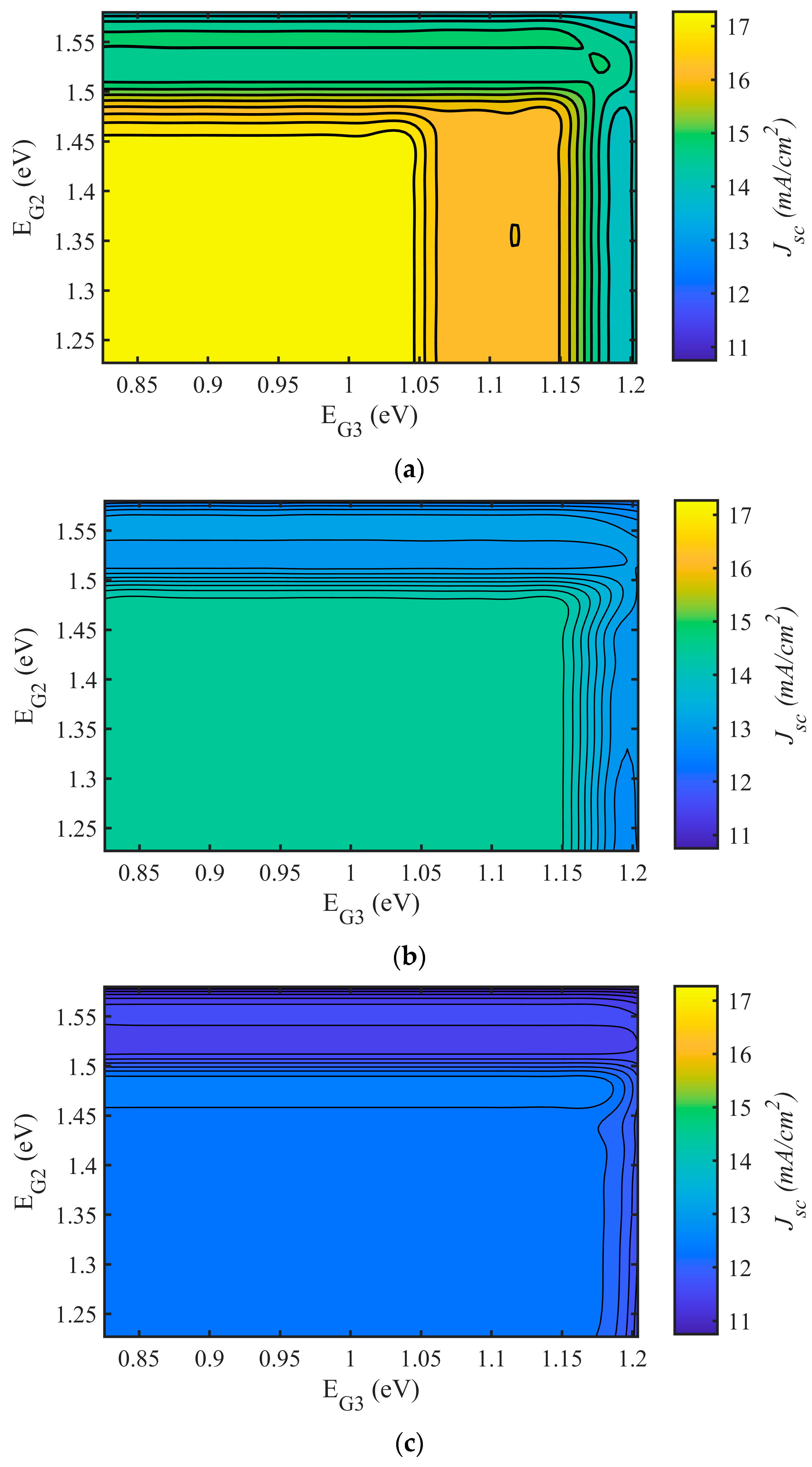
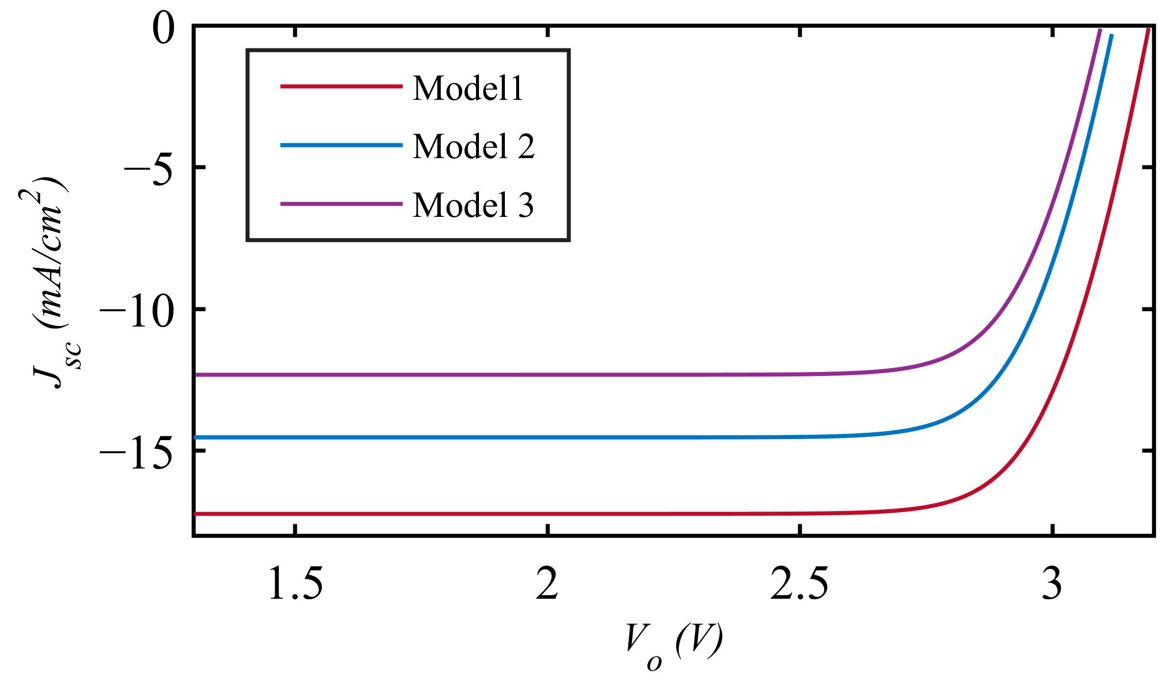
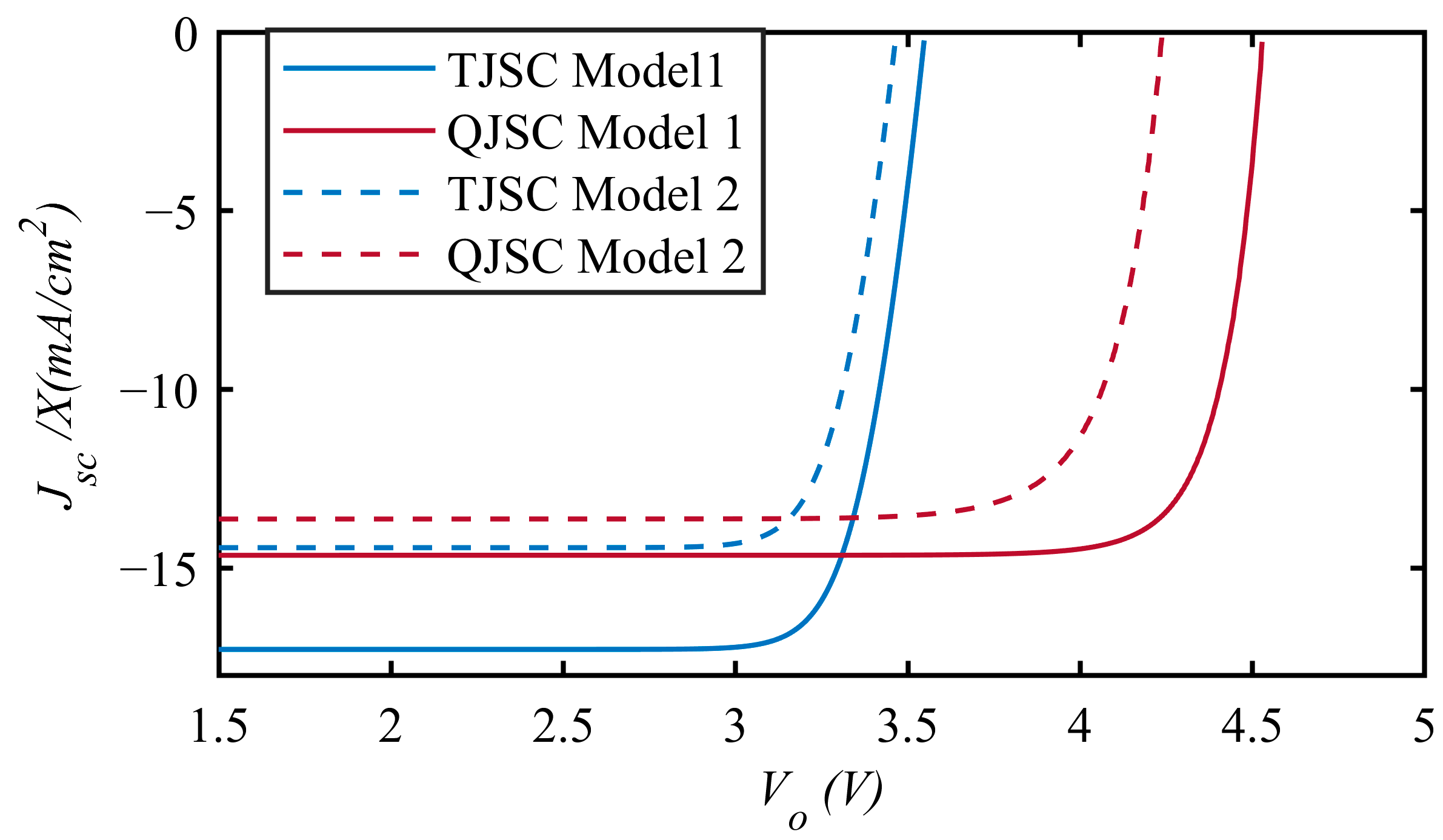
3.1. Triple Junction Cell Design

The nitrogen content in GaAsNP was changed and two different bandgap values of EG2 and EG3 were obtained for the middle and bottom subcells of TJSC. The efficiency variation due to EG2 and EG3 for Models 1, 2, and 3 is given in Figure 3a–c, respectively. Maximum efficiencies of 48.9%, 40.6%, and 33.7% were achieved at EG2 = 1.45 eV and EG3 = 1.04 eV for Model 1, EG2 = 1.45 eV and EG3 = 1.15 eV for Model 2, and EG2 = 1.45 eV and EG3 = 1.17 eV for Model 3. In order to understand the efficiency variation, short circuit current density, Jsc- EG2, EG3, and open circuit voltage, Voc- EG2, EG3, graphs were also calculated, as seen in Figure 4 and Figure 5. For Model 1, Jsc saturates at 17.27 mA/cm2 when EG2 and EG3 are less than approximately 1.45 eV and 1.06 eV, respectively, and decreases when the bandgaps are outside the given energy range, as shown in Figure 4a. In a bandgap energy region where Jsc remains constant, Voc is still affected by the changing values of EG2 and EG3 that also affect efficiency. Voc increases as bandgap values increase, as seen in Figure 5. The highest efficiency is achieved by the largest bandgaps which provide short circuit current density saturation. The top subcell base layer thickness is optimized for nearly full absorption to 3 µm to achieve the highest current density. The base thicknesses of the middle and bottom subcells were adjusted to provide current matching. For the optimum bandgap values, middle and bottom subcell thicknesses were calculated as 2.3 µm and 2.4 µm, respectively, at which the related spectrum is almost fully absorbed. When the optimum bandgaps are not selected, a part of the incoming spectrum cannot be converted to electricity efficiently. For example, if the upper cells are larger than the optimum bandgaps, they limit the short circuit current density. This means that although the bottom cell with a low bandgap has the capacity to generate higher current densities, its current density is limited by the upper cells. Consequently, a part of the incoming spectrum is wasted.
The short circuit current density variation with bandgaps in Model 2 is similar to Model 1, as seen from Figure 4b. This time, Jsc saturates at 14.53 mA/cm2 when EG2 and EG3 are less than approximately 1.45 eV and 1.15 eV, respectively, and decreases when the bandgaps are outside the given energy range. The highest efficiency is again provided by the largest bandgap values in the saturation region. However, smaller Jsc, Voc and efficiency values are observed in Model 2. The decrement in Jsc is mostly the result of higher surface recombination velocity. Both surface recombination velocity and SRH lifetime values in Model 2 cause the open circuit voltage to decrease, as seen from Figure 5b. Top subcell base layer thickness is again optimized for nearly full absorption to 3 µm to achieve the highest current density. For the optimum bandgap values, middle and bottom subcell base thicknesses are adjusted to approximately 1.2 µm and 1.7 µm, respectively for current matching. In Model 2, both the absorbed spectrum could not be converted to electricity efficiently due to the recombination of carriers without contributing to the current, and some of the spectrum was not fully absorbed because the thicknesses of the middle and bottom cells were thinned out for current matching.
Unlike in Models 1 and 2, in Model 3, the top cell thickness chosen was not thick enough to provide full absorption because the diffusion distances of the minority carriers decreased due to their very short lifetimes. As seen from Figure 4c, Jsc remains constant at 12.52 mA/cm2 when EG2 is smaller than nearly 1.5 eV. The maximum possible EG3 value that can provide the saturation current was obtained as 1.17 eV. The base thicknesses providing current matching are 2 µm, 2.3 µm and 2 µm for the top, middle and bottom cells, respectively. There is a small decrement in open circuit voltage compared to Models 1 and 2, but the efficiency is limited due to the reduction in short circuit current density mostly caused by large surface recombination velocities. The J-Vo curves of the triple junction cells with the highest efficiency for Models 1–3 are seen in Figure 6, and the output parameters are given in Table 2 in comparison with the results presented in [27]. The decrease in short circuit current density for Models 2 and 3 can be clearly seen from the figure. There is also a slight reduction in FF. The decrement in open circuit voltage seems to be limited, but to obtain the highest efficiency, the bandgap of the bottom cell, EG3, is increased by an amount of 0.11 eV for Model 2 and 0.13 eV for Model 3. There is also a 0.05 eV increase in the bandgap of the middle cell, EG2.
If the results are compared with [27], thanks to the bandgap tunable middle and bottom cells, a higher short circuit current density was obtained for Model 1 in our study. Because the optimum bandgaps are smaller, the open circuit voltage is also less than the one calculated in [27]. However, a higher efficiency potential was achieved. For Models 2 and 3, [27] had more successful results. The difference between short circuit current densities was not significant, but the open circuit voltages used in this study were less than the ones in [27] even though the chosen bandgaps were very close to each other. This is the result of applying large Sn, Sp values and small τn, τp values to all subcells in this study whereas they were only applied to top and middle cells in [27], as expressed previously.
The reduction in efficiency for Model 3 was mostly caused by large surface recombination velocities. In order to see the potential of the TJSC structure with improved Sn, Sp values, two cases given in Table 3 were investigated and promising results were obtained for small lifetimes when optimum bandgap combinations of Models 1 and 2 were used for Case 1 and 2.
The EQE curves of each subcell for two models are given in Figure 7, and the total EQE curves can be seen in Figure 8. EQE is very close to 100% for all three subcells in Model 1, except for short wavelengths. The carriers generated by high energy photons (short wavelength) recombine at the surface, or the short circuit current, hence EQE reduces. The decrement in short wavelengths is larger for Models 2 and 3 because surface recombination rates are larger. EQE values for the middle and bottom subcells also decrease because of insufficient base thickness and large surface recombination velocity.

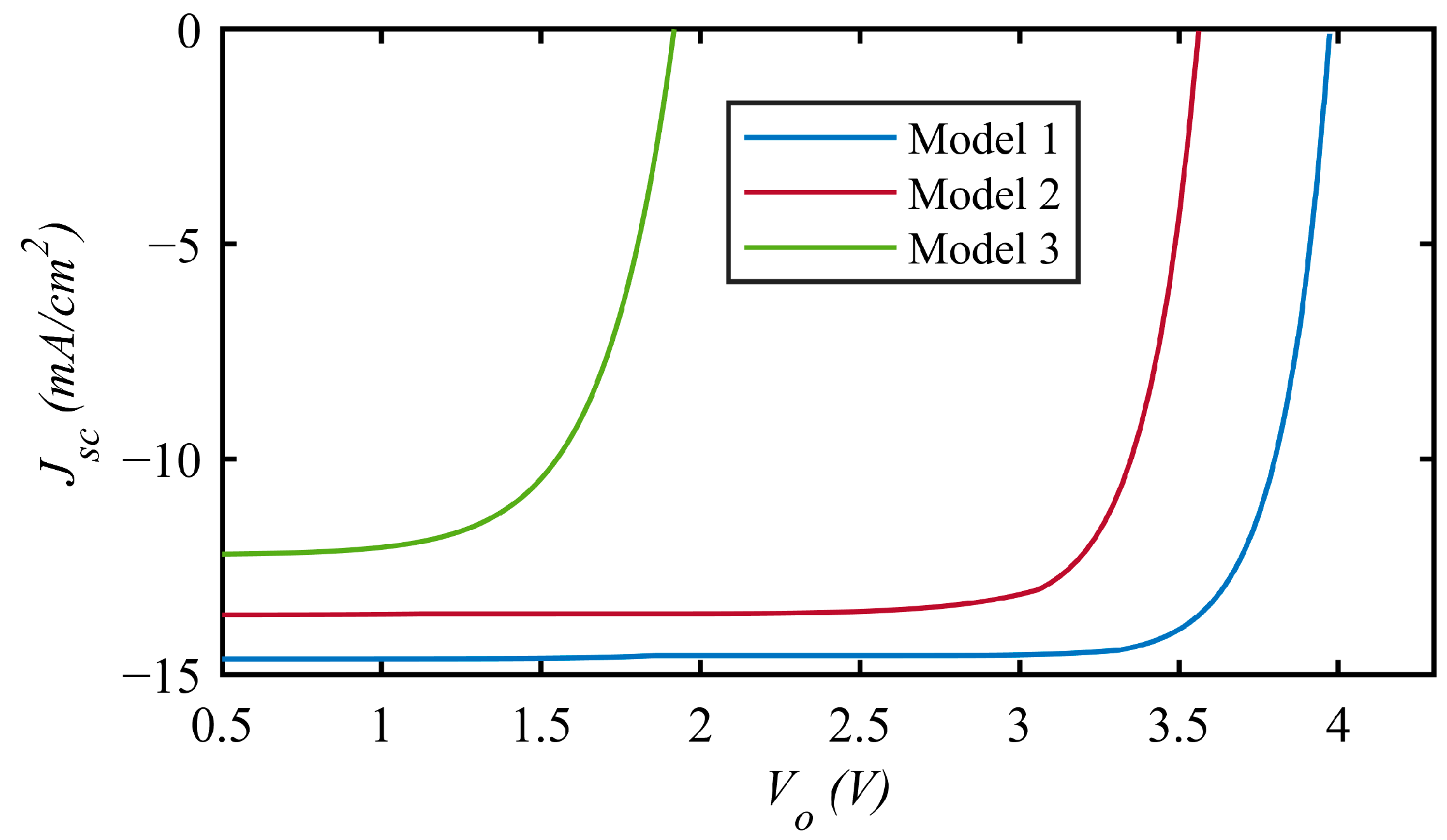
3.2. Quadruple Junction Cell Design

A GaAsNP junction was inserted into the MJSC system as the bottom cell and a quadruple junction structure was obtained. The efficiency performance of the resulting system was analyzed for Model 1 and 2. The fourth subcell was first chosen at the minimum possible value of 0.83 eV (N content equal to 7%) and the structure was investigated for the bandgap combinations that provided the highest efficiencies for the triple junction structure. Because the related part of the incoming spectrum was nearly fully absorbed by the optimized bandgap combination of the upper cells, the rest of the spectrum absorbed by the bottom cell was not enough to generate a current density matched to the upper cell current densities. Therefore, the bandgaps of the three subcells and the base thicknesses were optimized and matched to short circuit current densities of 14.64 mA/cm2 and 13.63 mA/cm2; open circuit voltages of 3.97 V and 3.56 V were obtained for Models 1 and 2 which yielded efficiencies of 48.9% and 39.9% which are close to the maximum efficiencies of the optimum triple junction structures. Despite the increase in open circuit voltage, the reduction in Jsc and the degradation in FF due to the small bandgap of the fourth junction caused the QJSC to be less efficient than the triple junction structure. Larger surface recombination rates and smaller lifetimes became much more effective for small bandgaps in the fourth junction for Model 3. Even if the short circuit current density was very close to the value obtained for TJSC, the huge reduction in FF from 88.3% to 67% and in open circuit voltage to 1.92 V caused the efficiency to decrease sharply to 15.73%. As a result, it can be said that if the carrier lifetimes are as small as the ones used in Model 3, small bandgap materials are not appropriate for MJSC. The J-Vo curves are given in Figure 9, and the optimum bandgap values can be seen in Table 4.
As seen from the EQE variations in Figure 10, a larger portion of solar spectrum is absorbed when compared to TJSC, but EQE of the top cell is decreased because the thickness of this cell is reduced to provide current matching. Similar to the triple junction structure, EQE values decreased in Models 2 and 3 due to higher surface recombination values.
The quadruple junction structure seems not to have an advantage over the triple junction structure. This is true for 1 sun illumination, but when sun concentration increases, the increment in output voltage provides an advantage for QJSC. A simple approach is used to include the effect of light concentration and carrier generation rates are multiplied by sun concentration, X, but the influence of high concentration on carrier mobilities and temperature is ignored. For very high concentration values, the nonlinearity terms of ΔnΔn and ΔpΔp should be included in Equations (1) and (2) and the reduction in mobilities should be taken into account. In [46], it is shown that ignoring nonlinearity terms causes more error when X is approximately higher than 1000 suns. Consequently, X is assumed to be 100 suns, which can be considered as a relatively small concentration value. Under 100-sun illumination, QJSC provides an efficiency of 58.6% and 49.5% for Models 1 and 2 whereas TJSC provides efficiencies of 54.9% and 44.7%, respectively. J-V curves and output parameters of QJSC and TJSC are given in Figure 11 and Table 5.
When the nonlinearity terms are included, Jsc was calculated to be nearly the same as the condition in which nonlinearity terms are ignored. The slight reduction in Voc caused the efficiency to decrease by an amount of 0.7%. The nonlinearity terms will be much more effective if the mobility degradation and temperature variation are taken into account. On the other hand, the series resistance, Rs, effect that is ignored in this study will be important for high concentrations. As a conclusion, the presented results can be accepted as a primary step for high concentration calculations. More detailed analysis is needed for future work.

4. Conclusions

A lattice matched triple junction solar cell on SiGe substrate with a GaAsP top cell and GaNAsP middle and bottom cells was investigated in this study. The advantage of GaNAsP material is its tunable bandgap. The content of nitrogen was changed and the efficiency variation of the triple junction solar cell was analyzed for Models 1–3. In Model 1, surface recombination velocities and SRH recombination lifetimes were given as Sn = 10 cm/s, Sp = 100 cm/s, τn = 100 ns and τp = 10 ns. A maximum efficiency of 48.92% was reached in Model 1 for EG2 = 1.45 eV and EG3 = 1.04 eV. When surface recombination velocities and SRH recombination lifetimes were given as Sn = 100 cm/s, Sp = 1000 cm/s, τn = 10 ns and τp = 1 ns for Model 2, the maximum efficiency obtained was 40.59% at EG2 = 1.45 eV and EG3 = 1.15 eV. In Model 3, the surface recombination velocities and SRH recombination lifetimes used were Sn = 1000 cm/s, Sp = 10000 cm/s, τn = 1 ns, and τp = 0.1 ns. The optimum bandgap combination of EG2 = 1.5 eV and EG3 = 1.17 eV achieved a maximum efficiency of 33.7%.
EQE curves were also calculated, and it was observed that the optimum bandgap combination in Model 1 provided almost full absorption in the related wavelength range. In Models 2 and 3, EQE decreased due to large surface recombination velocities and thinned base thicknesses due to current matching.
A quadruple solar cell structure was also investigated. The fourth bottom cell contributed to the open circuit voltage but caused a significant decrease in Jsc and FF. Therefore, no efficiency improvement was obtained under 1 sun illumination. On the other hand, it provided higher efficiency under 100-sun concentration.
The theoretical efficiency potential for MJSCs with SiGe substrate and bandgap tunable lattice matched GaNAsP junctions was calculated in this study. The results would be useful for future high efficiency MJSCs.

Funding

The author declares that no funds, grants, or other support were received during the preparation of this manuscript.

Institutional Review Board Statement

Not applicable.

Informed Consent Statement

Not applicable.

Data Availability Statement

The datasets used and/or analyzed during the current study are available from the corresponding author on reasonable request.

Conflicts of Interest

The author declares no conflict of interest.

References

  1. Green, M.A.; Dunlop, H.D.; Hohl-Ebinger, J.; Yoshita, M.; Kopidakis, N.; Hao, X. Solar cell efficiency tables (Version 61). Prog. Photovolt. Res. Appl. 2023, 31, 3–16. [Google Scholar] [CrossRef]
  2. Battaglia, C.; Cuevas, A.; De Wolf, S. High-efficiency crystalline silicon solar cells: Status and perspectives. Energy Environ. Sci. 2016, 9, 1552–1576. [Google Scholar] [CrossRef]
  3. Yoshikawa, K.; Yoshida, W.; Irie, T.; Kawasaki, H.; Konishi, K.; Ishibashi, H.; Asatani, T.; Adachi, D.; Kanematsu, M.; Uzu, H.; et al. Exceeding conversion efficiency of 26% by heterojunction interdigitated back contact solar cell with thin film Si technology. Sol. Energy Mater. Sol. Cells 2017, 173, 37–42. [Google Scholar] [CrossRef]
  4. Richter, A.; Hermle, M.; Glunz, S.W. Reassessment of the limiting efficiency for crystalline silicon solar cells. IEEE J. Photovolt. 2013, 3, 1184–1191. [Google Scholar] [CrossRef]
  5. Supplie, O.; Romanyuk, O.; Koppka, C.; Steidl, M.; Nägelein, A.; Paszuk, A.; Winterfeld, L.; Dobrich, A.; Kleinschmidt, P.; Runge, E.; et al. Metalorganic vapor phase epitaxy of III–V-on-silicon: Experiment and theory. Prog. Cryst. Growth Charact. Mater. 2018, 64, 103–132. [Google Scholar] [CrossRef]
  6. Essig, A.S.; Allebee, C.; Remo, T.; Geisz, J.F.; Steiner, M.A.; Horowitz, K.; Barraud, L.; Ward, J.S.; Schnabel, M.; Descoeudres, A.; et al. Raising the one-sun conversion efficiency of III–V/Si solar cells to 32.8% for two junctions and 35.9% for three junctions. Nat. Energy 2017, 2, 17144. [Google Scholar] [CrossRef]
  7. Yang, V.K.; Groenert, M.E.; Taraschi, G.; Leitz, C.W.; Pitera, A.J.; Currie, M.T.; Cheng, Z.; Fitzgerald, E.A. Monolithic integration of III-V optical interconnects on Si using SiGe virtual substrates. J. Mater. Sci. Mater. Electron. 2002, 13, 377–380. [Google Scholar] [CrossRef]
  8. Groenert, M.E.; Leitz, C.W.; Pitera, A.J.; Yang, V.; Lee, H.; Ram, R.J.; Fitzgerald, E.A. Monolithic integration of room-temperature cw GaAs/AlGaAs lasers on Si substrates via relaxed graded GeSi buffer layers. J. Appl. Phys. 2003, 93, 362–367. [Google Scholar] [CrossRef]
  9. Luan, H.; Lim, D.R.; Lee, K.K.; Chen, K.M.; Sandland, J.G.; Wada, K.; Kimerling, L.C. High-quality Ge epilayers on Si with low threading-dislocation densities. Appl. Phys. Lett. 1999, 75, 2909–2911. [Google Scholar] [CrossRef]
  10. Lew, K.L.; Yoon, S.F.; Loke, W.K.; Tanoto, H.; Dohrman, C.L.; Isaacson, D.M.; Fitzgerald, E.A. High gain AlGaAsGaAs heterojunction bipolar transistor fabricated on SiGeSi substrate. J. Vac. Sci. Technol. B Microelectron. Nanometer Struct. 2007, 25, 902–905. [Google Scholar] [CrossRef]
  11. Ginige, R.; Corbett, B.; Modreanu, M.; Barrett, C.; Hilgarth, J.; Isella, G.; Chrastina, D.; Von Känel, H. Characterization of Ge-on-Si virtual substrates and single junction GaAs solar cells. Semicond. Sci. Technol. 2006, 21, 775–780. [Google Scholar] [CrossRef]
  12. Kim, T.W.; Albert, B.R.; Kimerling, L.C.; Michel, J. InGaP solar cell on Ge-on-Si virtual substrate for novel solar power conversion. J. Appl. Phys. 2018, 123, 085111. [Google Scholar] [CrossRef]
  13. Lueck, M.R.; Andre, C.L.; Pitera, A.J.; Lee, M.L.; Fitzgerald, E.A.; Ringel, S.A. Dual junction GalnP/GaAs solar cells grown on metamorphic SiGe/Si substrates with high open circuit voltage. IEEE Electron. Device Lett. 2006, 27, 142–144. [Google Scholar] [CrossRef]
  14. García, I.; Barrutia, L.; Dadgostar, S.; Hinojosa, M.; Johnson, A.; Rey-Stolle, I. Thinned GaInP/GaInAs/Ge solar cells grown with reduced cracking on Ge|Si virtual substrates. Sol. Energy Mater. Sol. Cells 2021, 225, 111034. [Google Scholar] [CrossRef]
  15. Schmieder, K.J.; Gerger, A.; Diaz, M.; Pulwin, Z.; Ebert, C.; Lochtefeld, A.; Opila, R.; Barnett, A. Analysis of tandem III-V/SiGe devices grown on Si. In Proceedings of the 38th IEEE Photovoltaic Specialists Conference, Austin, TX, USA, 3–8 June 2012. [Google Scholar] [CrossRef]
  16. Caño, P.; Hinojosa, M.; García, I.; Beanland, R.; Marrón, D.F.; Ruiz, C.M.; Johnson, A.; Rey-Stolle, I. GaAsP/SiGe tandem solar cells on porous Si substrates. Sol. Energy 2021, 230, 925–934. [Google Scholar] [CrossRef]
  17. Caño, P.; Hinojosa, M.; Nguyen, H.; Morgan, A.; Marrón, D.F.; García, I.; Johnson, A.; Rey-Stolle, I. Hybrid III-V/SiGe solar cells grown on Si substrates through reverse graded buffers. Sol. Energy Mater. Sol. Cells 2020, 205, 110246. [Google Scholar] [CrossRef]
  18. Sabnis, V.; Yuen, H.; Wiemer, M. High-efficiency multijunction solar cells employing dilute nitrides. AIP Conf. Proc. 2012, 1477, 14–19. [Google Scholar] [CrossRef]
  19. Aho, A.; Isoaho, R.; Hytönen, L.; Aho, T.; Raappana, M.; Polojärvi, V.; Tukiainen, A.; Reuna, J.; Mäkelä, S.; Guina, M. Lattice-matched four-junction tandem solar cell including two dilute nitride bottom junctions. Prog. Photovolt. Res. Appl. 2019, 27, 299–305. [Google Scholar] [CrossRef]
  20. Aho, A.; Isoaho, R.; Raappana, M.; Aho, T.; Anttola, E.; Lyytikäinen, J.; Hietalahti, A.; Polojärvi, V.; Tukiainen, A.; Reuna, J.; et al. Wide spectral coverage (0.7–2.2 eV) lattice-matched multijunction solar cells based on AlGaInP, AlGaAs and GaInNAsSb materials. Prog. Photovolt. Res. Appl. 2021, 29, 869–875. [Google Scholar] [CrossRef]
  21. Isoaho, R.; Aho, A.; Tukiainena, A.; Aho, T.; Raappana, M.; Salminen, T.; Reuna, J.; Guina, M. Photovoltaic properties of low-bandgap (0.7–0.9 eV) lattice-matched GaInNAsSb solar junctions grown by molecular beam pitaxy on GaAs. Sol. Energ. Mat. Sol. C 2019, 195, 198–203. [Google Scholar] [CrossRef]
  22. Aho, A.; Isoaho, R.; Tukiainena, A.; Gori, G.; Campesato, R.; Guina, M. Dilute nitride triple junction solar cells for space applications: Progress towards highest AM0 efficiency. Prog. Photovolt. Res. Appl. 2018, 26, 740–744. [Google Scholar] [CrossRef]
  23. Levillayer, M.; Duzellier, S.; Massiot, I.; Arnoult, A.; Nuns, T.; Inguimbert, C.; Aicardi, C.; Parola, S.; Olivié, F.; Monflier, R.; et al. Degradation Study of InGaAsN p-i-n Solar Cell Under 1-MeV Electron Irradiation. IEEE Trans. Nucl. Sci. 2021, 68, 1694–1700. [Google Scholar] [CrossRef]
  24. Baranov, A.I.; Gudovskikh, A.S.; Kudryashov, D.A.; Lazarenko, A.A.; Morozov, I.A.; Mozharov, M.A.; Nikitina, E.V.; Pirogov, E.V.; Sobolev, M.S.; Zelentsov, K.S.; et al. Defect properties of InGaAsN layers grown as sub-monolayer digital alloys by molecular beam epitaxy. J. Appl. Phys. 2018, 123, 161418. [Google Scholar] [CrossRef]
  25. Isoaho, R.; Aho, T.; Aho, A.; Tukiainen, A.; Reuna, J.; Raappana, M.; Guinaet, M. High performance low-bandgap (0.8 eV) single junction GaInNAsSb solar cells incorporating Au-based back surface reflectors. Sol. Energ. Mat. Sol. C 2022, 234, 111413. [Google Scholar] [CrossRef]
  26. Murali, S.; Chikhalkar, A.; Zhang, C.; King, R.R.; Honsberg, C.B. Dilute nitride GaPNx as potential top cell candidate for Silicon based multijunction solar cells. In Proceedings of the 47th IEEE Photovoltaic Specialists Conference (PVSC), Calgary, AB, Canada, 15 June–21 August 2020. [Google Scholar] [CrossRef]
  27. Zhang, X.; Lin, K.; Xie, H.; Wang, Y. Theoretical study on potential performance of lattice-matched monolithic GaNP/GaNAsP/Si triple-junction solar cell. J. Phys. D 2020, 53, 445106. [Google Scholar] [CrossRef]
  28. Zhang, Y.; Yi, Y.; Li, W.; Liang, S.; Ma, J.; Cheng, S.; Yang, W.; Yi, Y. High Absorptivity and Ultra-Wideband Solar Absorber Based on Ti-Al2O3 Cross Elliptical Disk. Coatings 2023, 13, 531. [Google Scholar] [CrossRef]
  29. Wang, Z.; Liu, Y.; Li, L.; Zhu, D.; Yu, X.; Cheng, S.; Zheng, D.; Xiong, Y. An investigation of the effects of ZnO inverse opal pore size in the composite of ZnO nanorods/ZnO inverse opal on the performance of quantum dot-sensitized solar cells. Dalton Trans. 2023, 52, 81–89. [Google Scholar] [CrossRef]
  30. Zhao, F.; Lin, J.; Lei, Z.; Yi, Z.; Qin, F.; Zhang, J.; Liu, L.; Wu, X.; Yang, W.; Wu, P. Realization of 18.97% theoretical efficiency of 0.9 μm thick c-Si/ZnO heterojunction ultrathin-film solar cells via surface plasmon resonance enhancement. Phys.Chem. Chem. Phys. 2022, 24, 4871–4880. [Google Scholar] [CrossRef]
  31. Kudrawiec, R. Parameterization of the band gap energy for GaNxAs1-x-z Pz alloys. J. Appl. Phys. 2007, 101, 116101. [Google Scholar] [CrossRef]
  32. Navruz, T.S. Modeling lattice-matched InP-based multijunction solar cells. Turk. J. Electr. Eng. Co. 2017, 25, 1010–1020. [Google Scholar] [CrossRef]
  33. Nelson, J. Physics of Solar Cells; Imperial College Press: London, UK, 2003; pp. 145–169. [Google Scholar]
  34. Rey-Stolle, I.; García, I.; Barrigón, E.; Olea, J.; Pastor, D.; Ochoa, M.; Barrutia, L.; Algora, C.; Walukiewicz, W. On the thermal degradation of tunnel diodes in multijunction solar cells. In Proceedings of the 13th International Conference on Concentrator Photovoltaic Systems (CPV-13), AIP Conference Proceedings, Ottawa, ON, Canada, 6 September 2017; Volume 1881, p. 040005. [Google Scholar] [CrossRef]
  35. García, I.; Ochoa, M.; Lombardero, I.; Cifuentes, L.; Hinojosa, M.; Caño, P.; Rey-Stolle, I.; Algora, C.; Johnson, A.; Davies, I.; et al. Degradation of subcells and tunnel junctions during growth of GaInP/Ga(In)As/GaNAsSb/Ge 4-junction solar cells. Prog. Photovolt. Res. Appl. 2017, 25, 887–895. [Google Scholar] [CrossRef]
  36. Dawidowski, W.; Sciana, B.; Zborowska-Lindert, I.; Mikolasek, M.; Kova, J.; Tłaczała, M. Tunnel junction limited performance of InGaAsN/GaAs tandem solar cell. Sol. Energy 2021, 214, 632–641. [Google Scholar] [CrossRef]
  37. Walker, A.W.; Thériault, O.; Wilkins, M.M.; Wheeldon, J.F.; Hinzer, K. Tunnel-Junction-Limited Multijunction Solar Cell Performance Over Concentration. IEEE J. Sel. Top. Quantum Electron. 2013, 19, 1–8. [Google Scholar] [CrossRef]
  38. A NREL 2012 Reference Air Mass 1.5 Spectra (NREL 2012). Available online: https://www.nrel.gov/grid/solar-resource/spectra-am1.5.html (accessed on 10 February 2022).
  39. Vurgaftman, I.; Meyer, J.S.; Ram-Mohan, L.R. Band parameters for III–V compound semiconductors and their alloys. J. Appl. Phys. 2001, 89, 5815. [Google Scholar] [CrossRef]
  40. Levinshtein, M.; Rumyantsev, S.; Shur, M. Handbook Series on Semiconductor Parameters 1; World Scientific: London, UK, 1996. [Google Scholar]
  41. Dismukes, J.P.; Ekstrom, L.; Paff, R.J. Lattice Parameter and Density in Germanium-Silicon Alloys. J. Phys. Chem. 1964, 68, 3021–3027. [Google Scholar] [CrossRef]
  42. Jain, N.; Hudait, M.K. Impact of Threading Dislocations on the Design of GaAs and InGaP/GaAs Solar Cells on Si Using Finite Element Analysis. IEEE J. Photovolt. 2012, 3, 528–534. [Google Scholar] [CrossRef]
  43. Olson, J.M.; Ahrenkiel, R.K.; Dunlavy, D.J.; Keyes, B.; Kibbler, A.E. Ultralow recombination velocity at Ga0.5In0.5P/GaAs heterointerfaces. Appl. Phys. Lett. 1989, 55, 1208. [Google Scholar] [CrossRef]
  44. Geisz, J.F.; Reedy, R.C.; Keyes, B.M.W.; Metzger, K. Unintentional carbon and hydrogen incorporation in GaNP grown by metal-organic chemical vapor deposition. J. Cryst. Growth 2003, 259, 223–231. [Google Scholar] [CrossRef]
  45. Baranowski, M.; Kudrawiec, R.; Luce, A.V. Temperature evolution of carrier dynamics in GaNxPyAs1−y−xalloys. J. Appl. Phys. 2015, 117, 175702. [Google Scholar] [CrossRef]
  46. Navruz, T.S.; Saritas, M. Determination of the optimum material parameters for intermediate band solar cells using diffusion model. Prog. Photovolt. Res. Appl. 2014, 22, 593–602. [Google Scholar] [CrossRef]
Figure 1. Schematic structure of lattice matched TJSC cell on virtual SiGe substrate. C denotes the amount of doping concentration.
Photonics 10 00630 g001
Figure 2. Variation of SiGe lattice matched GaNAsP bandgap with nitrogen content.
Photonics 10 00630 g002
Figure 3. Efficiency variation of TJSC with bandgaps of middle and bottom subcells; EG2 and EG3 for (a) Model 1, (b) Model 2, (c) Model 3.
Photonics 10 00630 g003
Figure 4. Short circuit current density, Jsc variation of TJSC with bandgaps of middle and bottom subcells; EG2 and EG3 for (a) Model 1, (b) Model 2, (c) Model 3.
Photonics 10 00630 g004
Figure 5. Open circuit voltage, Voc variation of TJSC with bandgaps of middle and bottom subcells; EG2 and EG3 for (a) Model 1, (b) Model 2, (c) Model 3.
Photonics 10 00630 g005
Figure 6. J-Vo curve of TJSCs with highest efficiencies for Models 1–3.
Photonics 10 00630 g006
Figure 7. EQE curves of subcells for Models 1–3.
Photonics 10 00630 g007
Figure 8. EQE curves for the whole TJSC for Models 1–3.
Photonics 10 00630 g008
Figure 9. J-V curve of QJSCs with highest efficiencies for Models 1–3.
Photonics 10 00630 g009
Figure 10. EQE curves of subcells and the whole system of QJSC for Models 1–3. Total EQE curves are represented with dashed lines.
Photonics 10 00630 g010
Figure 11. J-V curves of TJSCs and QJSCs with highest efficiencies for Models 1 and 2 under 100-sun concentration.
Photonics 10 00630 g011
Table 1. Surface recombination velocity and lifetime values for Models 1–3 [27]. (S and τ values are assumed to be the same for all cells).
ParametersModel 1Model 2Model 3
Sn (cm/s)101001000
Sp (cm/s)100100010,000
τn (ns)100101
τp (ns)1010.1
Table 2. TJSC output parameters for optimum bandgap combination for Models 1–3 in comparison with the results of [27]. (EG1 = 1.95 eV).
ParametersModel 1Model 2Model 3
This Study[27]This Study[27]This Study[27]
EG2 (eV)1.451.481.451.471.51.48
EG3 (eV)1.041.12 (Si)1.151.12 (Si)1.171.12 (Si)
Jsc (mA/cm2)17.2714.3814.5314.1312.3212.46
Voc (V)3.193.393.153.263.13.17
FF (%)88.889.688.79088.391.6
Efficiency (%)48.943.740.641.533.736.2
Table 3. Output parameters of TJSC with improved Sn and Sp for small lifetimes.
Jsc (mA/cm2)Voc (V)FF (%)Efficiency (%)
Case 1: Sn = 10 cm/s, Sp = 100 cm/s and
τn = 1 ns, τp = 0.1 ns
16.722.9988.244.1
Case 2: Sn = 100 cm/s, Sp = 1000 cm/s and
τn = 1 ns, τp = 0.1 ns
14.533.186.938.9
Table 4. QJSC output parameters for optimum bandgap combination for Models 1–3. (EG1 = 1.95 eV).
ParametersModel 1Model 2Model 3
EG2 (eV)1.561.531.5
EG3 (eV)1.21.21.19
EG4 (eV)0.920.990.92
Jsc (mA/cm2)14.6413.6312.22
Voc (V)3.973.561.92
FF (%)84.182.767.0
Efficiency (%)48.939.915.73
Table 5. QJSC output parameters for optimum bandgap combination for Models 1 and 2.
ParametersModel 1Model 2
TJSCQJSCTJSCQJSC
Jsc/X(mA/cm2)17.2814.6414.5313.63
Voc (V)3.554.533.54.2
FF (%)89.488.487.986.5
Efficiency (%)54.958.644.749.5
Disclaimer/Publisher’s Note: The statements, opinions and data contained in all publications are solely those of the individual author(s) and contributor(s) and not of MDPI and/or the editor(s). MDPI and/or the editor(s) disclaim responsibility for any injury to people or property resulting from any ideas, methods, instructions or products referred to in the content.

