1. Introduction
Among the most common applications of photonic devices is using optical radiation for sensing of various parameters of materials including material composition, refractive index, thickness, and many others. Its use is incentivised by high sensitivity, low cost, electromagnetic immunity, and compactness just to name a few [
1]. A huge focus in this field is on surface plasmon resonance (SPR), which has gone through extensive research in many theoretical and experimental studies for its ability to provide real-time sensing of various physical, chemical, or biological quantities [
2,
3]. SPR sensors have been recognised as a highly promising platform for lab-on-chip bioanalytical sensing. They are well-known and widely used sensors for label-free analytical biosensing [
4].
The underlying principle behind SPR sensors is a resonant oscillation of electrons at the metal-dielectric boundary of a sensor, resulting in a dip in reflectivity [
5]. Various applications have originated from the utilisation of this selective spectral attenuation, from Kretschmann and Otto configurations [
6,
7], through waveguide, to fibre applications [
3]. In the case of Kretschmann/Otto configuration, extensive research brought even better sensitivity and selectivity by introduction of various stacked metal or dielectric layers complimenting basic metal nano-film [
8,
9,
10]. However, while SPR sensors based on Otto or Kretschmann configurations are usually unfit for integration due to their size or the necessity to use a prism coupling for SPR, waveguide-coupled SPR sensors provide suitable alternative thanks to their ease of use, significantly smaller footprint, and suitability for integration with other photonic components while theoretically maintaining sufficient sensitivity [
11].
Since the early 90s when waveguide-based SPR sensors were first introduced [
12,
13,
14], they have undergone extensive research in terms of applications, design, sensitivity improvement, etc. Even though single-mode waveguides are generally the most commonly used while promoting excellent sensitivity [
15], one of the research goals in this work was to show that multimode waveguides should be able to operate using the same principle, with comparable sensitivity and higher transmission rates. It is due to the fact that a higher number of modes offer a much higher probability of SPR excitation on the waveguide-metal/metal-analyte interface. While such applications are already proposed in the works of Chu et al. [
16] or Walter et al. [
17], these applications either utilise only planar waveguides, therefore rendering them impossible to use in more complex circuits or lab-on-chip, or offer sensitivity for only very limited range of analyte’s refractive indices.
The sensor proposed in this work utilises three-dimensional confinement, which allows its use in photonic integrated circuits (PICs), and also takes advantage of SiON material platform by utilising material’s refractive index (RI) adjustability, to offer the best possible solution for RI of any commonly used liquid analyte (RI anywhere between 1.2–1.6 [
18]).
2. Materials and Methods
The proposed sensor is a waveguide-based plasmonic refractive index sensor with a direct interface between a metallic layer and waveguiding core. The material platform Si
3N
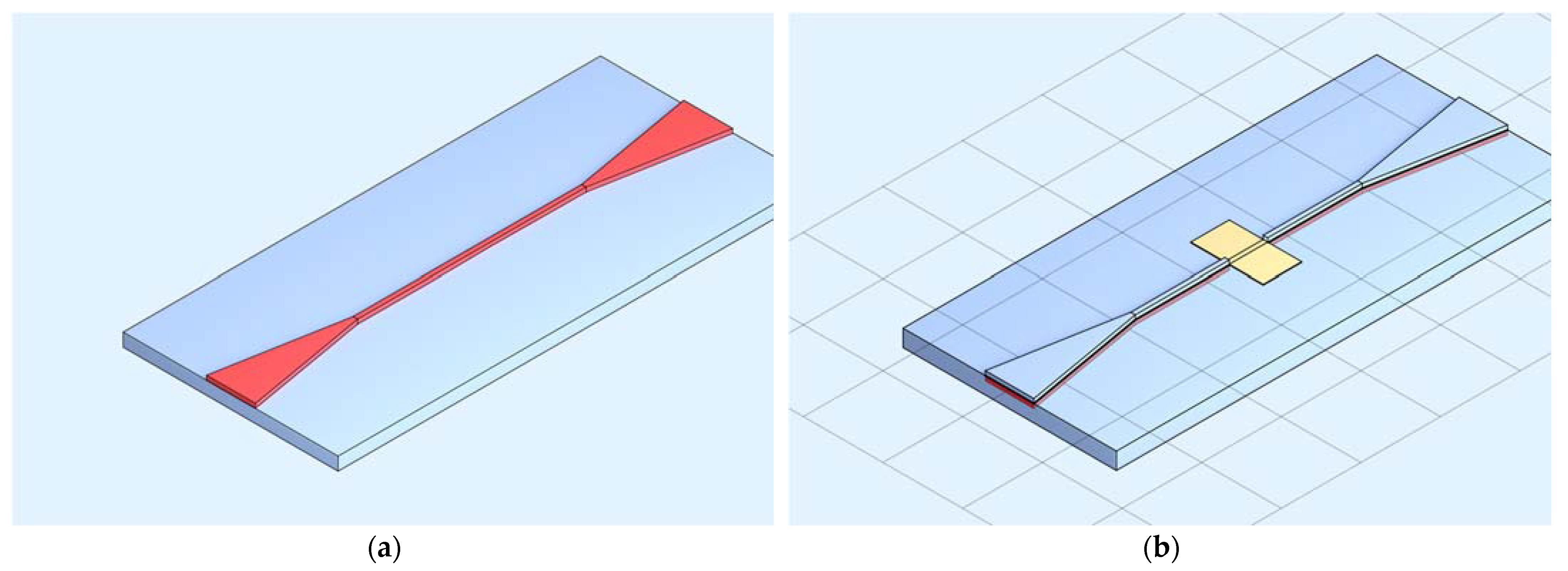
4/SiON was chosen, due to its transparency for visible wavelength range as well as tunability of refractive index which proves to be a key parameter in the design of this sensor type. The 3D structure of the sensor is shown in
Figure 1 for both pure waveguide design with coupling tapers and after gold layer deposition and passivation. It consists of a multimode waveguide with a cross-section of 8 × 8 µm
2, input and output taper and a gold layer 5 mm long and 45 nm thick.
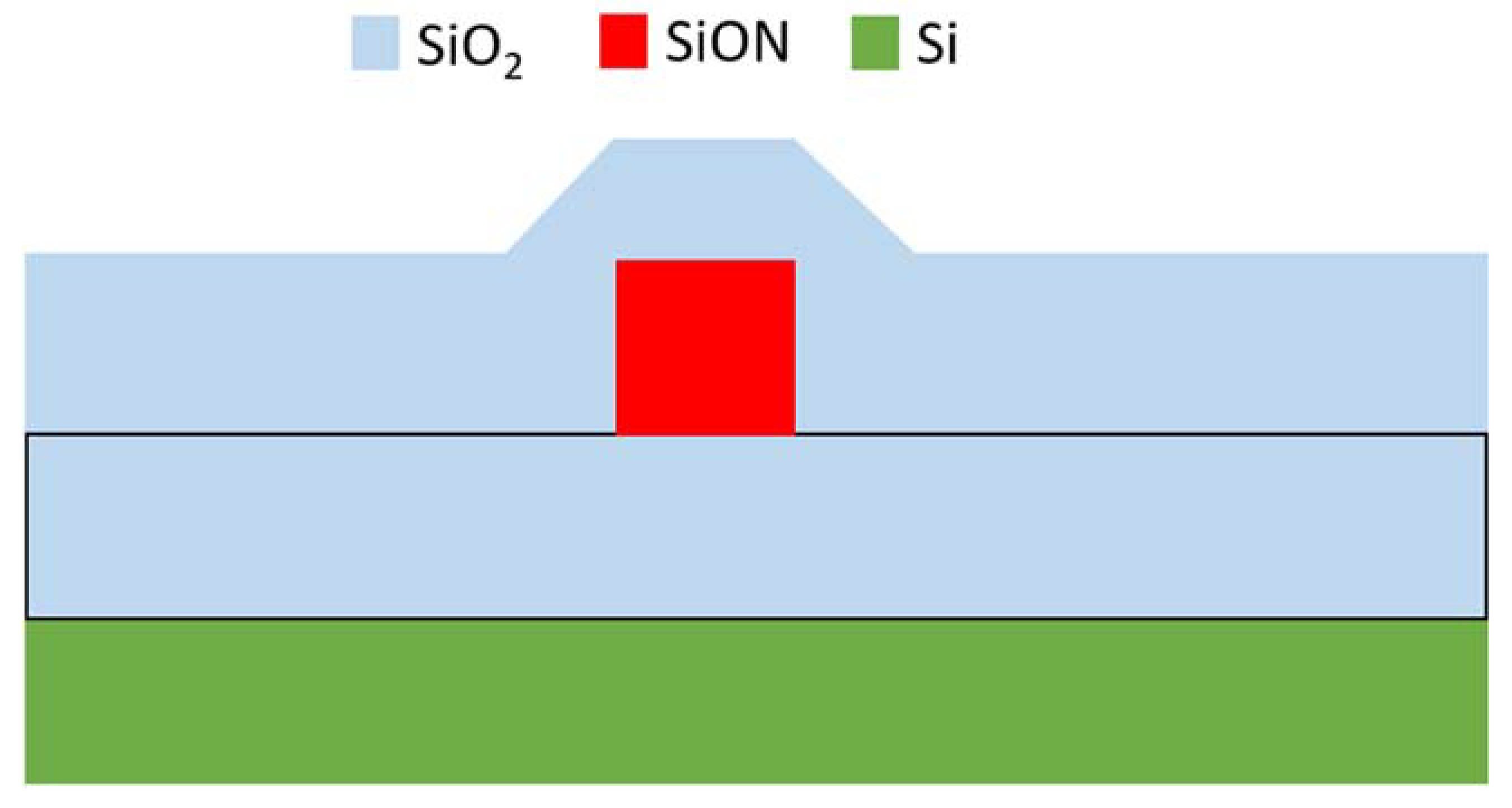
The cross-section of the proposed material platform is shown in
Figure 2 where a silicon wafer was chosen as a substrate for the device, on top of which the SiO
2 buffer layer with a thickness of 6–10 µm is expected to be grown by available methods like plasma enhanced chemical vapour deposition. On the top of the buffer layer, SiON material is expected to be grown using the same growth method, while adjusting the parameters to obtain desired refractive index. Finally, the whole waveguide is to be passivated by a thick layer of SiO
2 to prevent analyte’s interaction with the non-sensing part of the waveguide.
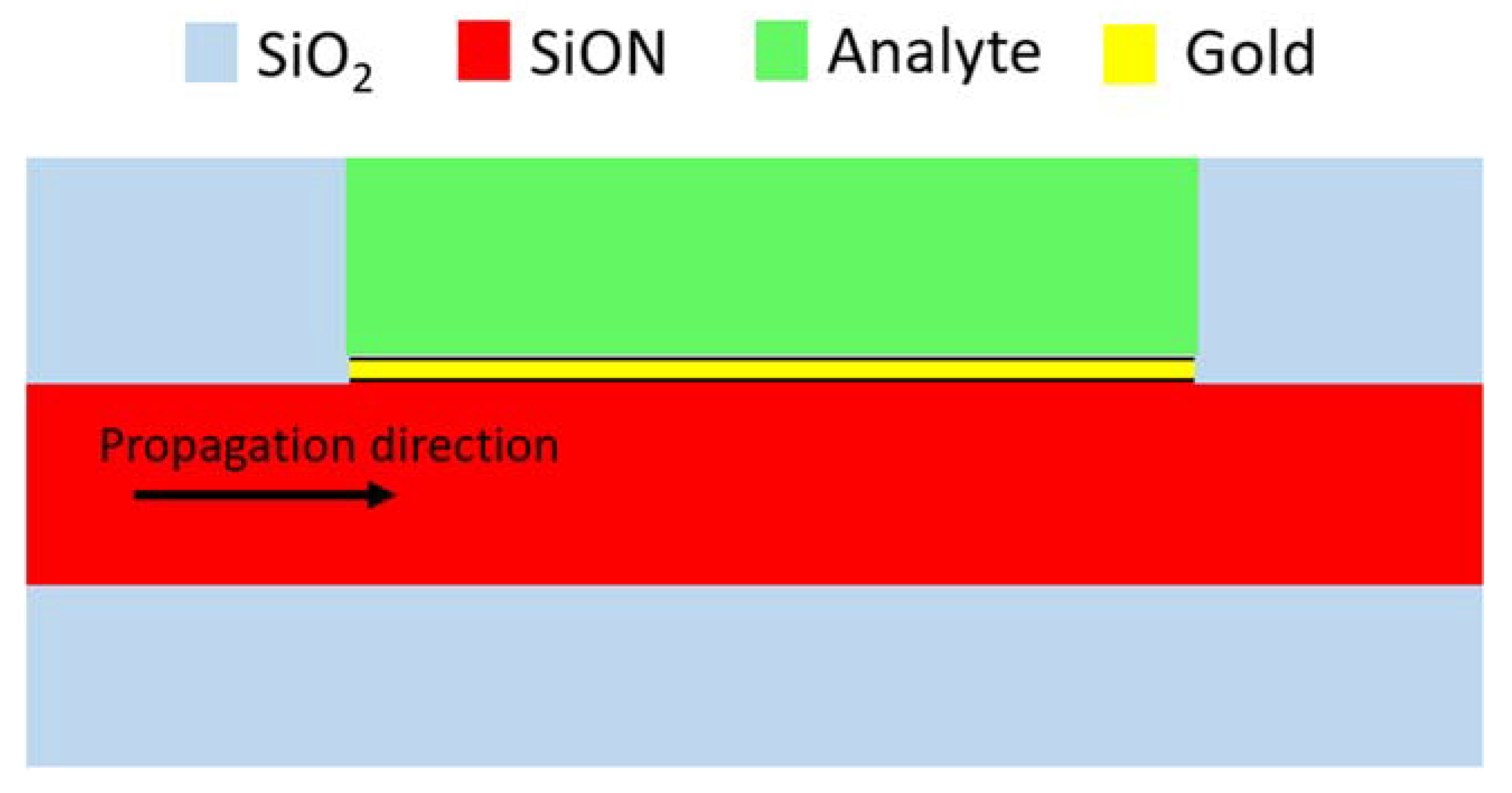
The final structure of the sensor consisting of four distinct layers is shown in
Figure 3, with the SiO
2 cladding layers (
n = 1.46) thick enough to optically separate the waveguiding layer from the Si substrate and environment, waveguiding layer (SiON), and a gold layer on top of core in the sensing part. Gold has been chosen as the metallic layer due to its strong plasmonic resonance capabilities combined with chemical stability in various environments.
According to the work of Čtyroký et al. [
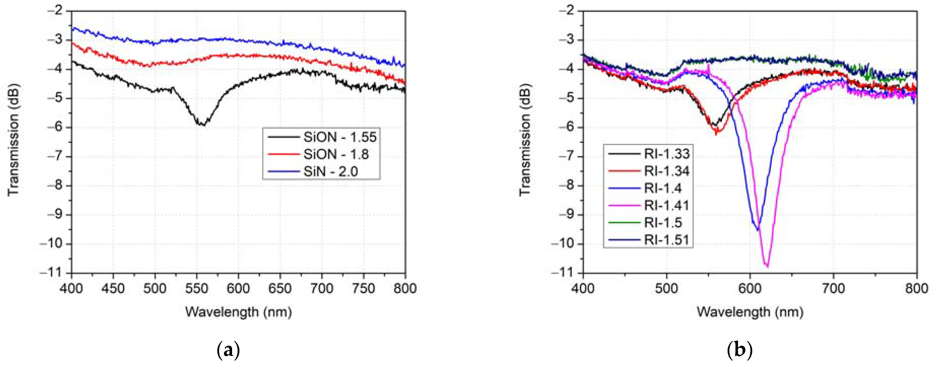
19] for this type of sensor, due to its underlying physical principle the position and attenuation of a dip in a spectrum are highly dependent on both refractive indices of an analyte, as well as the waveguiding core. Therefore, in order to maintain good sensitivity with spectral dip occurring in visible wavelengths, the sensor must consist of a waveguiding core with a refractive index similar to the refractive index of the analyte This hypothesis is verified in
Figure 4, where spectral characteristics of transmission through the proposed waveguide sensor are shown. The refractive index of the analyte for this investigation was chosen to represent water-based solutions, e.g.,
n = 1.33. As a light source, a 50 µm wide beam with a Gaussian profile was chosen to represent direct coupling with multi-mode fibre and to neglect the offset for the possibility of lacking excitation for some modes, due to the fibre position. While transmission spectra of waveguide cores with refractive indices of 2.0 (pure Si
3N
4) and 1.8 (SiON) do not exhibit any differentiable dip, for the waveguiding core with a refractive index of 1.55 (still well in the range of possibilities of SION material platform [
20,
21]) the spectrum exhibits strong dip between 500 and 600 nm of wavelength. Such core was used to analyse the influence of the analyte’s index of refraction variation with a significant shift corresponding to the change.
Figure 4b shows also the increased sensitivity of a sensor with a refractive index of core 1.55 proving the verity of the rule concerning analyte and core refractive index matching. It points out increased sensitivity for aqueous solutions while showing the prohibition of the use for analytes with RI above 1.5 due to confinement constraints. For these initial simulations, a SiON waveguide with (8 × 8) µm
2 profile with a 45 µm thick gold layer was used.
The sensor part with plasmonic structure was designed and simulated using the Eigenmode Expansion Method incorporated into the ModePROP module of RSoft Photonic Device Tools due to its computational simplicity synergizing well with a relatively long waveguiding model as well as with its ability to solve photonic calculations including the plasmonic effect.
3. Results
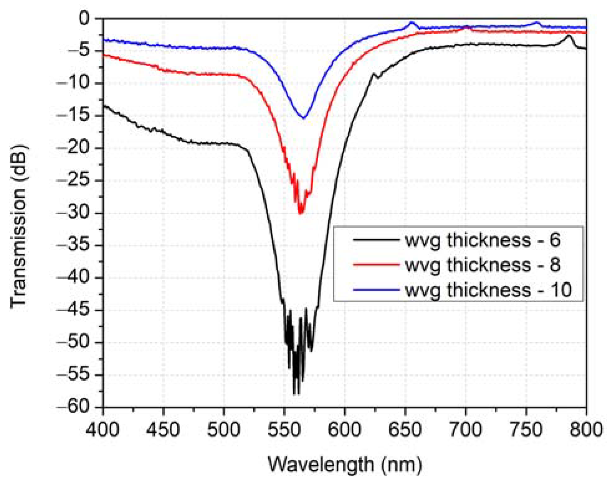
After deciding on the structure design, the thickness of the waveguide, gold layer length, and its thickness were optimized to maximise sensitivity and transmission. While optimising other waveguide dimensions, such as the waveguide width, the simulation result showed no significant change in sensor functionality apart from a slight change in total transmitted power. Therefore, all the following simulations were carried out using a 2D model, which enables the use of finer mesh, while maintaining relatively short simulation times and low computational demands. As shown in
Figure 5, the thicker the waveguiding layer, the higher the transmission through the waveguiding sensor. While for the waveguide thickness of 4 or 6 µm, there is strong attenuation for a wide range of lower wavelengths, for waveguide thickness of 8 µm and 10 µm, respectively, there are pronounced resonance dips as well as sufficient transmission through the sensor structure. A thickness of 8 µm was chosen for further optimisation due to its satisfactory transmission combined with minimising the thickness of the material grown.
Consequently, the plasmonic layer itself was investigated and optimised. Firstly, its length was of an interest. Even though the thickness of the waveguide plays a role in the amount of light transmitted through the sensor waveguide, a fixed thickness of 8 µm was chosen as a fixed point with an initial gold layer thickness of 45 nm due to its common use in Kretschmann and Otto configuration applications and layer length of 5 mm. An aqueous solution with a refractive index of 1.33 was used as an analyte for the simulations. In
Figure 6 are shown spectral dependencies of transmitted power through the waveguide on the length of the gold plasmonic layer. As expected, there is a decrease in overall transmission due to plasmonic attenuation with increasing length, accompanied by a slight improvement in definition on the plasmonic dip. Although with a more defined dip, the sensitivity might be improved, a 5 mm length of a gold layer was deemed long enough to offer good ease of use while still maintaining a relatively small footprint.
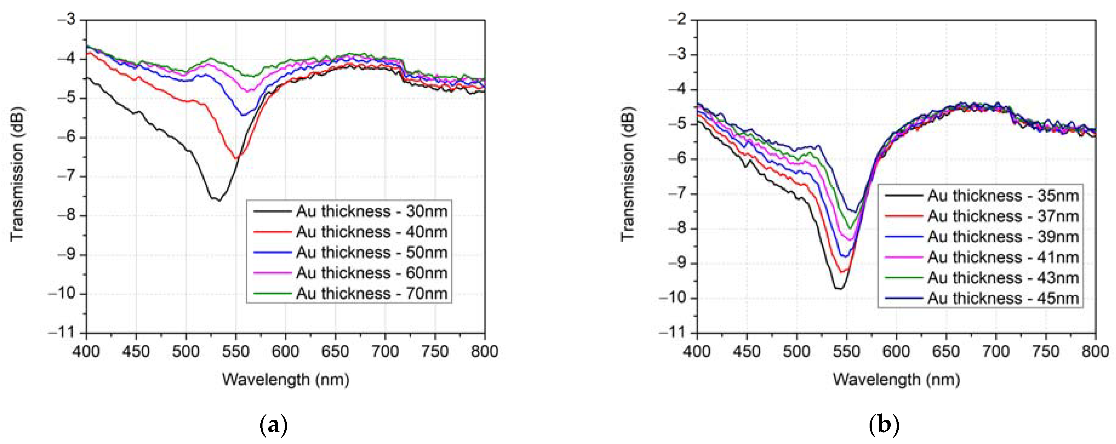
The last parameter optimised was the thickness of the gold layer. The simulation results showed that gold thickness influences not only the depth of resonance dip but its spectral position as well. This knowledge allows us to optimise waveguide-based sensor not only for the analyte’s refractive index but for the desired central wavelength as well. The results are shown in
Figure 7 where it can be seen that the thickness of 60 nm is already preventing optical wave penetration to the analyte’s side and weakens the occurrence of plasmonic dip; therefore, any gold layer used for the sensor has to be thinner. On the other hand, we can conclude that plasmonic dip is too broad in the spectrum for thickness below 30 nm which limits its applicability applicable in sensors. The thickness of 40 nm was, after closer investigation (
Figure 7b), chosen as the optimal value for future simulations. This thickness was chosen to avoid influence of gold absorption for wavelengths lower than 500 nm as well as to maintain plasmonic dip definition.
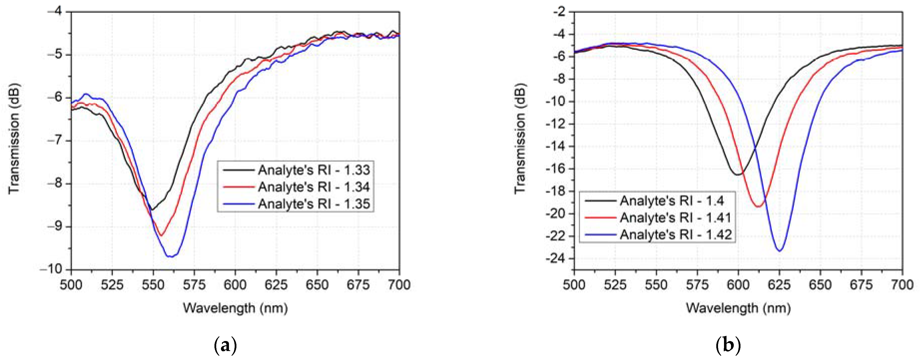
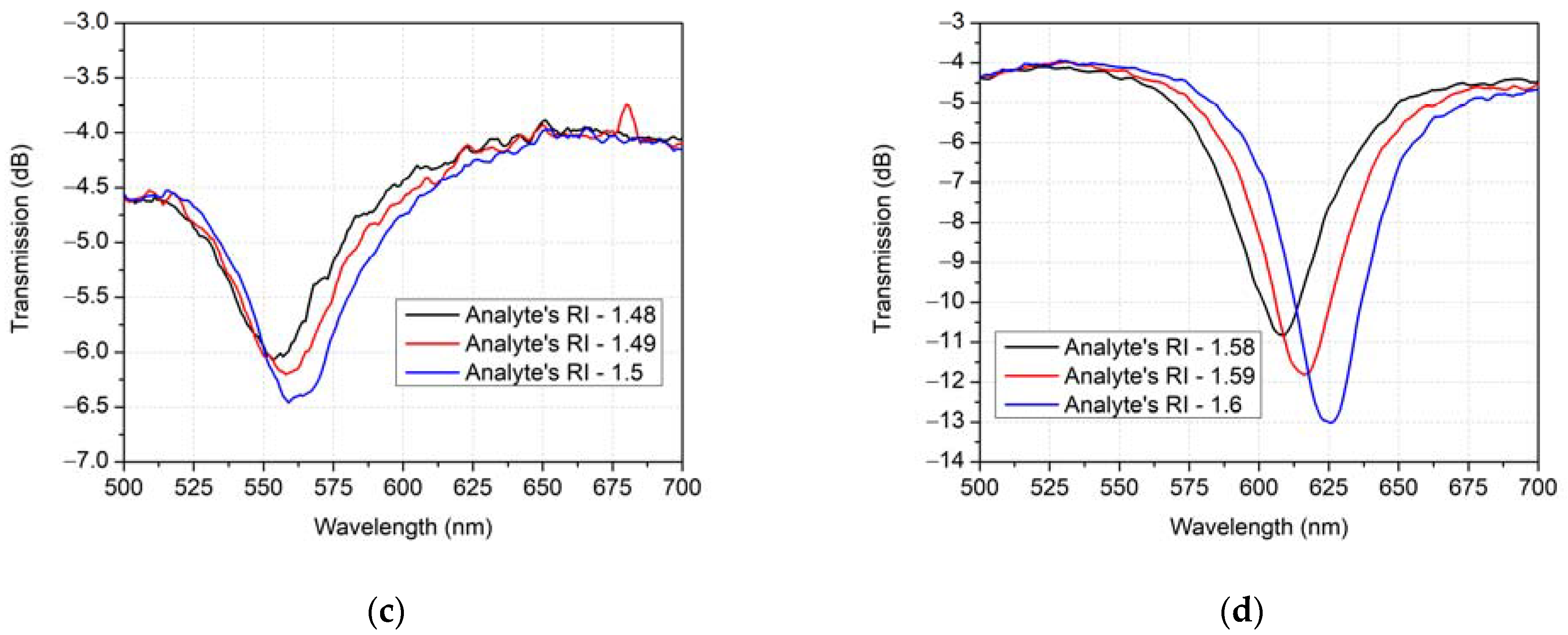
To maintain fabrication simplicity as well as minimize the amount of optimization necessary for sensor fabrication, the selected parameters of gold layer and waveguide thickness were kept unchanged for all following sensor variations. Consequently, two SPR sensors suitable for detection of different liquid analytes are proposed, with the only difference being the refractive index of their respective cores, as the two optimal values of the core’s RI 1.55 and 1.8 were chosen with the aim of covering all the liquid analytes with refractive indices from 1.3 to 1.6 (liquid analytes with RI of 1.2 to 1.3 are rarely used; however, if the necessity arises, sensitivity for them can still be obtained by proposed sensor structure). Their transmitted optical power spectra for different refractive index ranges are shown in
Figure 8.
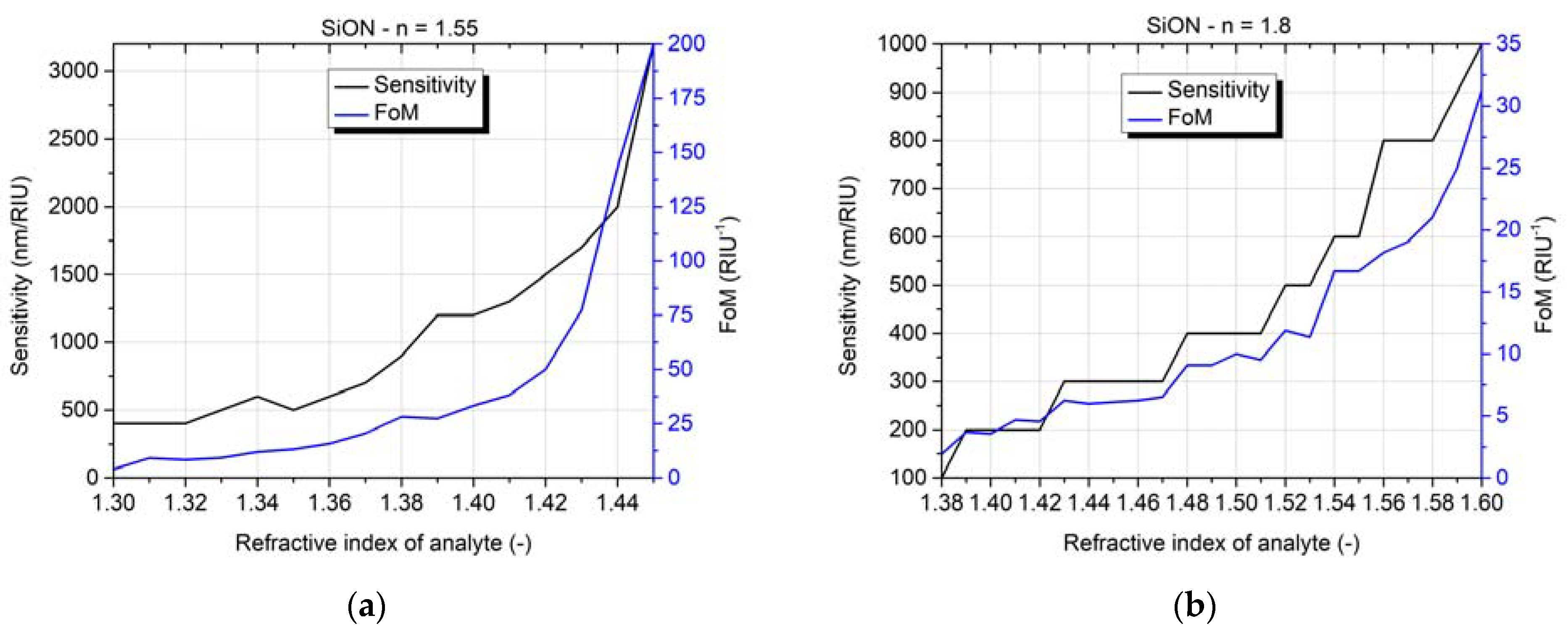
For better visualisation, sensitivity, and Figure of Merit, dependence on the refractive index of the analyte is shown in
Figure 9. It can be seen that both of these parameters are nonlinear, where with the analyte’s RI approaching the refractive index of the core, the spectral shift is increasing. According to simulation results, the sensitivity of the sensor (calculated as theoretical spectral shift corresponding to a change of refractive index of analyte by one unit) with the core’s refractive index of 1.55 is approximately 500 nm/RIU (Refractive Index Unit) for a lower range while improving to more than 3000 nm/RIU for higher ranges. On the other hand, if the sensor is adjusted to be sensitive for analytes with refractive indices over 1.5 (therefore changing the core’s RI to 1.8) the presented sensitivity is approximately 200 nm/RIU and 1000 nm/RIU, respectively. As mentioned before, it shows strong nonlinearity (which corresponds to increased sensitivity) while the refractive index of analyte approaches that of the waveguide’s core.
4. Discussion
The simulation model presented in this work uses an approximation of multimode fibre input field, by using a wide Gaussian beam. This approach, however, does not ensure the propagation of all modes in the input part of the waveguide sensor. The results, therefore, might not reflect spectral measurements of the finished structure. Discrepancies might stem from multimode fibres used to couple in and out of the waveguide, where even the small position change of these fibres relative to the waveguide might cause excitation of different modes in the multimode waveguide sensor structure. This excitation of different modes might cause not only lower sensitivity but also a small shift in plasmonic dip minima. However, all the coupling and mode propagation issues could be overcome in future work, by introducing the proposed sensor into a photonic circuit, therefore removing the variability of inconsistent input coupling.
The simulation results also show something perceived as noise in the spectra. This “pseudo-noise” is a direct result of RSoft suite computational workflow used with Eigen-mode Expansions Method. The simulation suite, instead of using a broad-spectrum light source, calculates spectral response by scanning through each individual wavelength separately. This fact, in combination with inherent simulation approximation by using a grid, might result in small discrepancies in results for even very close wavelengths. Although this “pseudo-noise” does have an effect on resulting spectra, it is negligible in regard to SPR dip attenuation and spectral position.
The result shows that the two proposed sensors are able to cover range of analytes with a refractive index from 1.3 to 1.6. The first sensor with a refractive index of core 1.55 offers sensitivity for RI from 1.3 to 1.44. The upper limit stems from the spectral dip minimum being too wide to be accurately determined. This constraint might be overcome by shortening the gold layer length, at the cost of losing sensitivity for lower refractive indices. The second proposed sensor with a core RI of 1.8 covers the rest of possible liquid analytes with a sensitivity from 1.38 to 1.6. As shown in
Figure 9, the potential achievable sensitivity of the sensor is more than 3000 nm/RIU, and Figure of Merit obtained from simulations was more than 200 RIU
−1. This value matches commonly used waveguide and SPR-based refractive index sensors in terms of sensitivity and even overcomes them in terms of Figure of Merit [
22,
23]. In addition, its multimode character offers the possibility of a relatively long sensing structure with relatively low attenuation to provide ease of use in a non-lab environment. The proposed sensor’s potential sensitivity is more than four times higher than Bragg gratings [
24], silicon [
25], and MIM structures [
22] while boasting also comparable or even higher FoM. Higher sensitivity was usually proposed only using more complex structures like ring resonators [
22] or by the introduction of multi-stack layers into the design [
15] which might also be a possible future area of research for the sensor proposed in this paper.
Finally, spectra presenting the sensitivity of the sensor show strong nonlinearity which only further proves that sensitivity increases more rapidly while approaching the waveguide’s refractive index, thus, promoting the adjustability of SION material platform to balance the sensor’s sensitivity and loss by adjusting the RI parameter of the core. With a refractive index of the SiON material platform ranging from values of SiO2 (1.456) to Si3N4 (2.0 for visible wavelengths), it can be said that the platform as well as the design should be capable of sensing any commonly used liquid analyte.
5. Conclusions
The optimal design of the SPR-multimode waveguide sensor based on the SiON material platform, consisting of a multimode waveguide and a thin layer of gold, and its main optical characteristics are presented in this work. Its design provides insusceptibility to analyte application accuracy, usually attributed only to planar sensors (with sensing length of 5 mm), while maintaining good sensitivity and integrability onto PICs and offering adjustability in accordance with analyte refractive index. To prove the versatility of the design, two variations of the same sensor, with only the refractive index of SiON layer difference, are presented and investigated. Both proposed variations show non-linear sensitivity which rises to more than 3000 nm/RIU and FoM of more than 200 RIU−1 even without any sensitivity-enhancing structure on top of the gold layer. In combination, they prove to be sensitive to any aqueous analyte’s refractive index varied in a range of 1.3–1.6, which provides versatility for multiple sensing applications. This sensor, therefore, shows great potential and versatility towards lab-on-chip applications, while the possibility of future sensitivity and selectivity improvements by various metamaterials or complex stacked structures remains a subject for further research. These results show promising signs for future use of this sensor in photonic integrated circuits combining insusceptibility of planar structures, integrability of waveguide circuits, adjustability to analyte’s RI, and CMOS fabrication compatibility.
Author Contributions
Conceptualization, M.F. and J.K.; methodology, M.F. and M.Z.; software, M.Z. and A.K.; validation, J.K. and A.K.; formal analysis, M.Z.; investigation, M.F.; resources, J.K., A.K. and F.U.; data curation, M.F. and M.Z.; writing—original draft preparation, M.F.; writing—review and editing, M.Z., J.K. and F.U.; visualization, M.F.; supervision, J.K. and F.U.; project administration, J.K.; funding acquisition, J.K. and A.K. All authors have read and agreed to the published version of the manuscript.
Funding
This work was supported by the Slovak Research and Development Agency under project No. APVV-20-0437, and by the grant agency of the Ministry of Education, Science, Research and Sport of the Slovak Republic (VEGA 1/0733/20).
Institutional Review Board Statement
Not applicable.
Informed Consent Statement
Not applicable.
Data Availability Statement
Not applicable.
Conflicts of Interest
The authors declare no conflict of interest.
References
- Ferreira, M.F.S.; Castro-Camus, E.; Ottaway, D.J.; López-Higuera, J.M.; Feng, X.; Jin, W.; Jeong, Y.; Picqué, N.; Tong, L.; Reinhard, B.M.; et al. Roadmap on Optical Sensors. J. Opt. 2017, 19, 083001. [Google Scholar] [CrossRef] [PubMed]
- Prabowo, B.A.; Purwidyantri, A.; Liu, K.-C. Surface Plasmon Resonance Optical Sensor: A Review on Light Source Technology. Biosensors 2018, 8, 80. [Google Scholar] [CrossRef]
- Yesudasu, V.; Pradhan, H.S.; Pandya, R.J. Recent Progress in Surface Plasmon Resonance Based Sensors: A Comprehensive Review. Heliyon 2021, 7, e06321. [Google Scholar] [CrossRef]
- Wang, J.; Sanchez, M.M.; Yin, Y.; Herzer, R.; Ma, L.; Schmidt, O.G. Silicon-Based Integrated Label-Free Optofluidic Biosensors: Latest Advances and Roadmap. Adv. Mater. Technol. 2020, 5, 1901138. [Google Scholar] [CrossRef]
- Chen, Y.; Ming, H. Review of Surface Plasmon Resonance and Localized Surface Plasmon Resonance Sensor. Photonic Sens. 2012, 2, 37–49. [Google Scholar] [CrossRef]
- Zhu, J.; Li, N. Novel High Sensitivity SPR Sensor Based on Surface Plasmon Resonance Technology and IMI Waveguide Structure. Results Phys. 2020, 17, 103049. [Google Scholar] [CrossRef]
- Shibayama, J.; Mitsutake, K.; Yamauchi, J.; Nakano, H. Kretschmann- and Otto-type Surface Plasmon Resonance Waveguide Sensors in the Terahertz Regime. Microw. Opt. Technol. Lett. 2021, 63, 103–106. [Google Scholar] [CrossRef]
- Hayashi, S.; Nesterenko, D.V.; Sekkat, Z. Waveguide-Coupled Surface Plasmon Resonance Sensor Structures: Fano Lineshape Engineering for Ultrahigh-Resolution Sensing. J. Phys. Appl. Phys. 2015, 48, 325303. [Google Scholar] [CrossRef]
- Yang, L.; Wang, J.; Yang, L.; Hu, Z.-D.; Wu, X.; Zheng, G. Characteristics of Multiple Fano Resonances in Waveguide-Coupled Surface Plasmon Resonance Sensors Based on Waveguide Theory. Sci. Rep. 2018, 8, 2560. [Google Scholar] [CrossRef]
- Du, W.; Zhao, F. Silicon Carbide Based Surface Plasmon Resonance Waveguide Sensor with a Bimetallic Layer for Improved Sensitivity. Mater. Lett. 2017, 186, 224–226. [Google Scholar] [CrossRef]
- Dostálek, J.; Čtyroký, J.; Homola, J.; Brynda, E.; Skalský, M.; Nekvindová, P.; Špirková, J.; Škvor, J.; Schröfel, J. Surface Plasmon Resonance Biosensor Based on Integrated Optical Waveguide. Sens. Actuators B Chem. 2001, 76, 8–12. [Google Scholar] [CrossRef]
- Čtyroký, J.; Homola, J.; Lambeck, P.V.; Musa, S.; Hoekstra, H.J.W.M.; Harris, R.D.; Wilkinson, J.S.; Usievich, B.; Lyndin, N.M. Theory and Modelling of Optical Waveguide Sensors Utilising Surface Plasmon Resonance. Sens. Actuators B Chem. 1999, 54, 66–73. [Google Scholar] [CrossRef]
- Weiss, M.N.; Srivastava, R.; Groger, H.; Lo, P.; Luo, S.-F. A Theoretical Investigation of Environmental Monitoring Using Surface Plasmon Resonance Waveguide Sensors. Sens. Actuators Phys. 1995, 51, 211–217. [Google Scholar] [CrossRef]
- Harris, R.D.; Wilkinson, J.S. Waveguide Surface Plasmon Resonance Sensors. Sens. Actuators B Chem. 1995, 29, 261–267. [Google Scholar] [CrossRef]
- Mishra, S.K.; Zou, B.; Chiang, K.S. Surface-Plasmon-Resonance Refractive-Index Sensor With Cu-Coated Polymer Waveguide. IEEE Photonics Technol. Lett. 2016, 28, 1835–1838. [Google Scholar] [CrossRef]
- Chu, Y.-S.; Hsu, W.-H.; Lin, C.-W.; Wang, W.-S. Surface Plasmon Resonance Sensors Using Silica-on-Silicon Optical Waveguides. Microw. Opt. Technol. Lett. 2006, 48, 955–957. [Google Scholar] [CrossRef]
- Walter, J.-G.; Eilers, A.; Alwis, L.S.M.; Roth, B.W.; Bremer, K. SPR Biosensor Based on Polymer Multi-Mode Optical Waveguide and Nanoparticle Signal Enhancement. Sensors 2020, 20, 2889. [Google Scholar] [CrossRef]
- Reis, J.C.R.; Lampreia, I.M.S.; Santos, Â.F.S.; Moita, M.L.C.J.; Douhéret, G. Refractive Index of Liquid Mixtures: Theory and Experiment. ChemPhysChem 2010, 11, 3722–3733. [Google Scholar] [CrossRef]
- Čtyroký, J.; Homola, J.; Skalský, M. Tuning of Spectral Operation Range of a Waveguide Surface Plasmon Resonance Sensor. Electron. Lett. 1997, 33, 1246–1248. [Google Scholar] [CrossRef]
- Wörhoff, K.; Hilderink, L.T.H.; Driessen, A.; Lambeck, P.V. Silicon Oxynitride. J. Electrochem. Soc. 2002, 149, F85. [Google Scholar] [CrossRef]
- Podlucký, Ľ.; Vincze, A.; Kováčová, S.; Chlpík, J.; Kováč, J.; Uherek, F. Optimization of Fabrication Process for SiON/SiOx Films Applicable as Optical Waveguides. Coatings 2021, 11, 574. [Google Scholar] [CrossRef]
- Faruque, M.O.; Al Mahmud, R.; Sagor, R.H. Highly Sensitive Plasmonic Refractive Index Sensor Using Doped Silicon: An Alternative to MIM Structures. Plasmonics 2022, 17, 203–211. [Google Scholar] [CrossRef]
- Kumar, M.; Kumar, A.; Tripathi, S.M. Optical Waveguide Biosensor Based on Modal Interference between Surface Plasmon Modes. Sens. Actuators B Chem. 2015, 211, 456–461. [Google Scholar] [CrossRef]
- Saha, N.; Brunetti, G.; Kumar, A.; Armenise, M.N.; Ciminelli, C. Highly Sensitive Refractive Index Sensor Based on Polymer Bragg Grating: A Case Study on Extracellular Vesicles Detection. Biosensors 2022, 12, 415. [Google Scholar] [CrossRef] [PubMed]
- Steglich, P.; Bondarenko, S.; Mai, C.; Paul, M.; Weller, M.G.; Mai, A. CMOS-Compatible Silicon Photonic Sensor for Refractive Index Sensing Using Local Back-Side Release. IEEE Photonics Technol. Lett. 2020, 32, 1241–1244. [Google Scholar] [CrossRef]
| Disclaimer/Publisher’s Note: The statements, opinions and data contained in all publications are solely those of the individual author(s) and contributor(s) and not of MDPI and/or the editor(s). MDPI and/or the editor(s) disclaim responsibility for any injury to people or property resulting from any ideas, methods, instructions or products referred to in the content. |
© 2023 by the authors. Licensee MDPI, Basel, Switzerland. This article is an open access article distributed under the terms and conditions of the Creative Commons Attribution (CC BY) license (https://creativecommons.org/licenses/by/4.0/).
