Communication

Numerical Method for the Design of Compact Adiabatic Devices with Multiple Parameter Variations

1
School of Information Science and Technology, Nantong University, Nantong 226019, China
2
Research Center for Intelligent Information Technology, Nantong University, Nantong 226019, China
3
School of Computer and Information Engineering, Xinjiang Agricultural University, 311 Nongda Dong Lu, Urumqi 830052, China
4
Nantong Key Laboratory of Advanced Microwave Technology, Nantong University, Nantong 226019, China
5
School of Pharmacy, Nantong University, Nantong 226019, China
6
School of Physics, University of Electronic Science and Technology of China, Chengdu 610054, China
*
Authors to whom correspondence should be addressed.
Photonics 2023, 10(5), 517; https://doi.org/10.3390/photonics10050517
Submission received: 16 March 2023 / Revised: 20 April 2023 / Accepted: 26 April 2023 / Published: 1 May 2023

Abstract

:
In this study, a numerical method for designing efficient adiabatic devices with multiple structural parameter variations (NAMSP) is developed. This method can be applied to a wide range of devices based on adiabatic mode evolution structures. The numerical design complexity of multiple structural parameter variations will be greatly improved compared to the case of a single parameter variation. Therefore, an efficient domain decomposition scheme was originally introduced into the NAMSP method. The proposed method can help compute compact adiabatic guided-wave shapes for these adiabatic devices with multiple structural parameter variations. Adiabatic devices with multiple structural parameter variations are used to connect different complex waveguides, which are often difficult to design using analytical methods. The design involves tapering the width of the two or more core layers at one time; however, this change in the width typically affects the mode both vertically and horizontally. Our numerical method allows the shape of the width variation for each layer that facilitates compact adiabatic mode transformation to be obtained. The efficiency of the adiabatic device that was designed using the NAMSP method considerably exceeds that obtained using a linear-shaped device. Moreover, our designed adiabatic device enables an ultra-wide operating bandwidth (spans in the wavelength from 1050 nm to 4780 nm).

1. Introduction

Silicon waveguides have received substantial attention because of their excellent mode confinement, low cost, and compatibility with CMOS processing technology [1]. Given these characteristics, a high-density integration and mass production of optical components can be achieved [2]. The silicon-on-insulator (SOI) ridge waveguide is a fundamental component in photonic integrated circuits (PICs) [3,4,5,6,7,8]. The adiabatic transfer of light beams between different waveguides is a very efficient way to achieve efficient power transfer. In the “adiabatic” mode evolution, the beam mode is changed slowly along the propagation direction. A general goal of adiabatic device design is the adiabatic transfer between different waveguide structures with different mode shapes.
This research developed as we tried to connect different waveguides with multiple structural parameter variations. The numerical design complexity of multiple structural parameter variations is greatly improved compared to the case of a single parameter variation. Figure 1 shows a simple example that involves applying the connecting mode device to adiabatic transfer of an optical mode from one ridge waveguide to another. During the process, the optical mode shape can either expand or shrink either horizontally or vertically in a three-dimensional (3D) space.
The design of the adiabatic device in this case involves simultaneously changing the width of the two core layers (such as the widths of the top core layer and middle core layer); however, this change in the width affects the mode both vertically and horizontally. A straightforward way to design an adiabatic device is to join one waveguide to another with a linear shape, but this requires an extremely long adiabatic device. Moreover, an overly long device reduces the device density and causes propagation losses. For example, J. H. Schmid et al. proposed a two-level adiabatic taper that was designed to couple light from the fundamental mode of a ridge waveguide to a narrow high aspect ratio slit-like channel waveguide [9]. The device consists of two parts: a two-level ridge and an adjacent slab waveguide structure. Furthermore, another mode connector design approach [10] proposed waveguide conversion structures that converted a ridge waveguide into a strip waveguide. To minimize the multimode effects, a bi-level taper structure between a ridge waveguide and a strip waveguide was also proposed [11]. However, the aforementioned methods are limited to simple structures. In cases where the geometry is more complicated, such as those that involve the variation or optimization of multiple structural parameters, it is difficult for such methods to solve the problem. Our previous study [12,13] proposed numerical design methods for the design of adiabatic devices, but the design of the adiabatic devices targeted by that study all involved only one structural parameter variation. As shown in Figure 2, if only the width of the top silicon taper waveguide varies, this presents a design problem with “single structural parameter variation”. If the width of the top silicon waveguide and the middle silicon waveguide are both changing, this presents a design problem with “multiple structural parameter variation”. To the best of our knowledge, the numerical design of adiabatic devices with multiple structural parameter variations has not been reported.
Thus, the present study develops a numerical method for the design of efficient adiabatic devices with multiple structural parameters variation (hereinafter referred to as NAMSP). This method minimizes the adiabatic device length segment-wise by maintaining a constant mode power loss along the device. The acronym “N” stands for numerical method, the acronym “A” stands for adiabatic devices, and “MSP” stands for multiple structural parameters. Put succinctly, we offer a numerical method for the design of efficient adiabatic devices with variations in multiple structural parameters. Furthermore, an efficient domain decomposition (DD) scheme is introduced into the NAMSP method. The DD scheme is a numerical calculation scheme that decomposes the whole structure into several subdomains and designs each subdomain separately. The method can be used easily by following a numerical procedure, and it generates a compact adiabatic guided-wave shape for adiabatic devices. The efficiency of the device designed using the NAMSP method is far better than that of the linear-shape case. In addition, the adiabatic device obtained through this method (see Section 3.2) has an ultra-broad operating bandwidth (~3880 nm centered at 2840 nm), which is a main area of interest in adiabatic device design.
The subsequent section details the case of a ridge waveguide to explain the algorithm for the NAMSP method and show that the device efficiency obtained is considerably better than that based on the linear-shape case.

2. Structure and Analysis

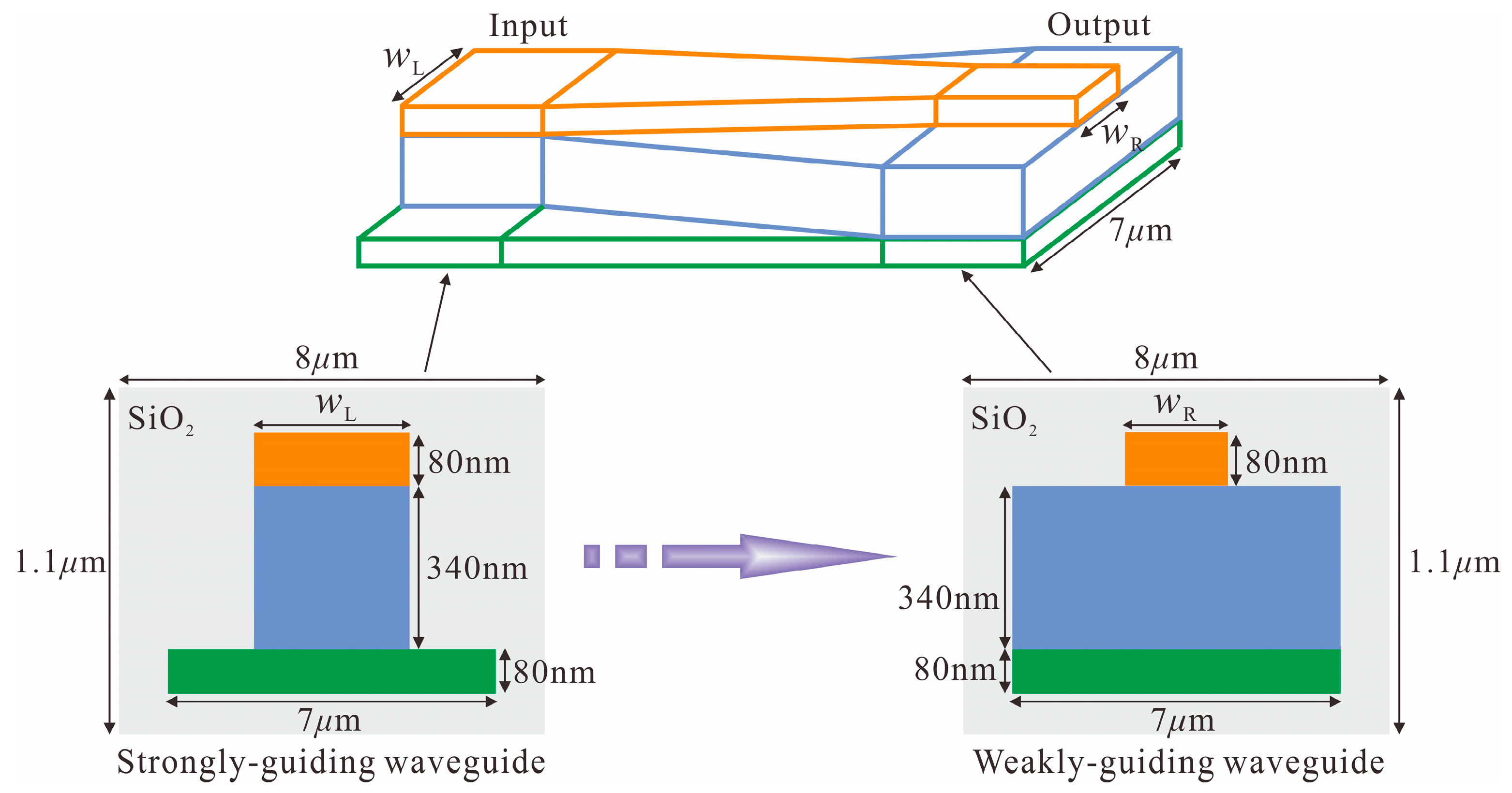
The adiabatic device connects the different waveguide structures, where the top silicon taper width is from wL to wR and the middle silicon taper width is from wL to 7 μm, as shown in Figure 2. Here, we assume an 80 nm-thick bottom silicon planar waveguide, a 340 nm-thick middle taper waveguide, and an 80 nm-thick top silicon taper waveguide (nSi = 3.455) surrounded by silicon dioxide (nSiO2 = 1.445). The width and height of the silicon dioxide in Figure 2 are 8 μm and 1.1 μm, respectively. The design of the device involves tapering the width of the two core layers (340 nm-thick middle taper waveguide and 80 nm-thick top silicon taper waveguide) at the same time. Figure 2 shows a simple linear shape design, wherein the initial waveguide width of wL is connected to the final waveguide width of wR with a linear taper for the top silicon taper, and the initial waveguide width of wL is connected to the final waveguide width of 7 μm with a linear taper for the middle silicon taper. The wavelength λ0 of light is 1.55 μm. In this study, the TE0 mode is considered. For the sake of description, the initial waveguide is called a strongly guiding waveguide, and the final waveguide is referred to as a weakly guiding waveguide.
When the strongly guiding waveguide and the weakly guiding waveguide are directly connected, the severe disparity between the mode field diameters of the strongly guiding waveguide and that of the weakly guiding waveguide will result in excessive coupling losses. Thus, the first step in achieving high transfer efficiency is to ascertain the optimal width wL and wR for the two waveguides that need to be connected. Therefore, we then calculate the effective refractive index (neff) and mode-field diameters (cH and cV) for the TE modes in the two waveguides. Here, we first determine the width wR = 2.85 μm for the weakly guiding waveguide and then ascertain the width wL for the strongly guiding waveguide. Using FDTD Solutions [14], the effective index neff, horizontal mode-field diameters cH, and vertical mode-field diameters cV of the fundamental mode (TE0 mode) for the weakly guiding waveguide can be obtained, as shown in Table 1. CH and CV are defined by the full width at 1/e maximum of the optical intensity in the horizontal and vertical directions.
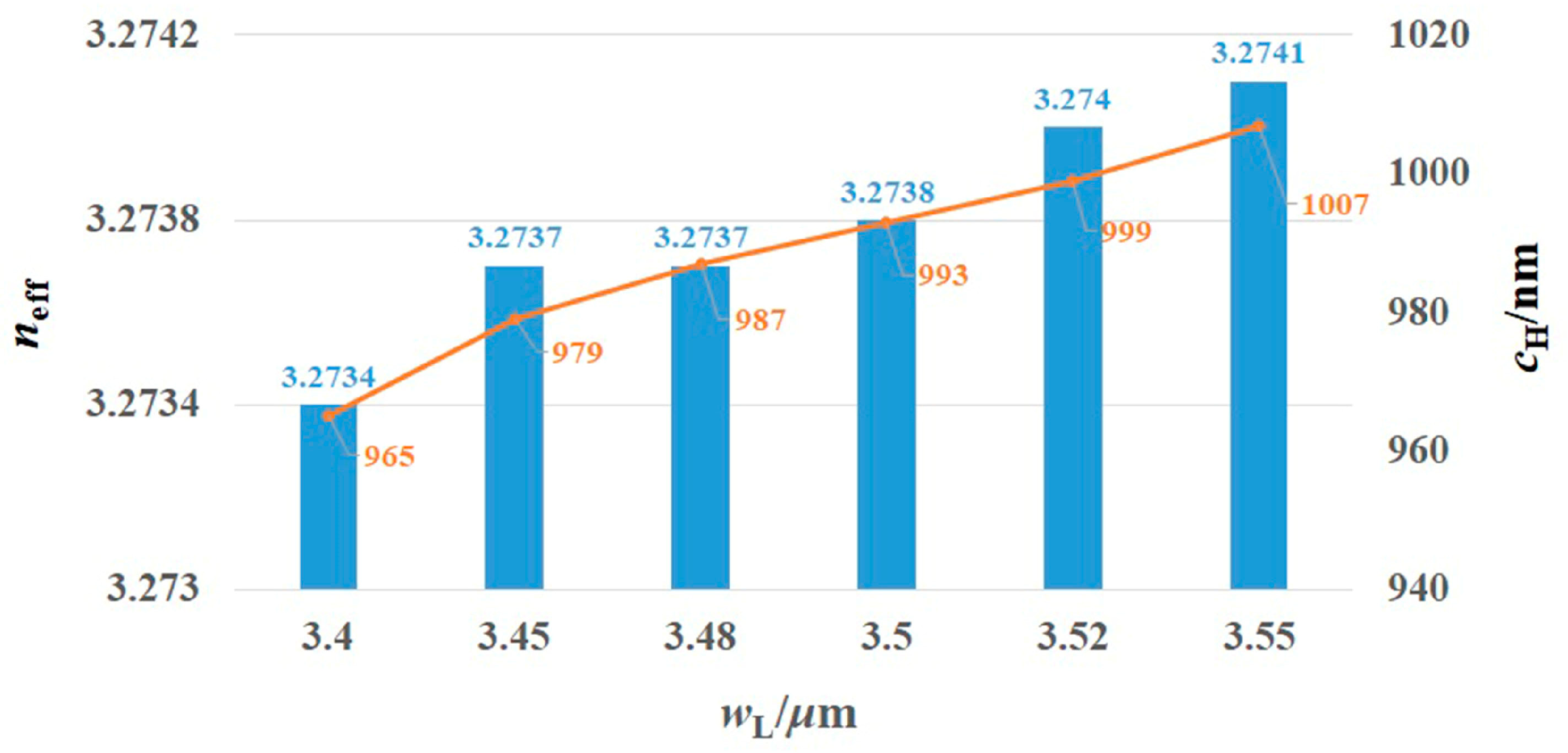
Subsequently, we changed the width w for the strongly guiding waveguide to obtain the values of neff, cH, and cV for the TE0 mode, as presented in Table 1. For easier visualization and understanding of Table 1, we plot in Figure 3 the trends of neff and cH variation with width wL in the strongly guiding waveguide. Table 1 and Figure 3 show that when wL = 3.50 μm in the strongly guiding waveguide, the effective index neff, horizontal mode-field diameter cH, and vertical mode-field diameter cV of the fundamental mode for the two waveguides are extremely close. Thus, when wL = 3.50 μm for the strongly guiding waveguide and wR = 2.85 μm for the weakly guiding waveguide, the two ridge waveguides have a suitable mode match.
Here, we provide an example to demonstrate how to obtain the best matching width for two different waveguides. The matching width for other cases can be obtained in a similar manner.

3. Description of the NAMSP Method for the Adiabatic Device

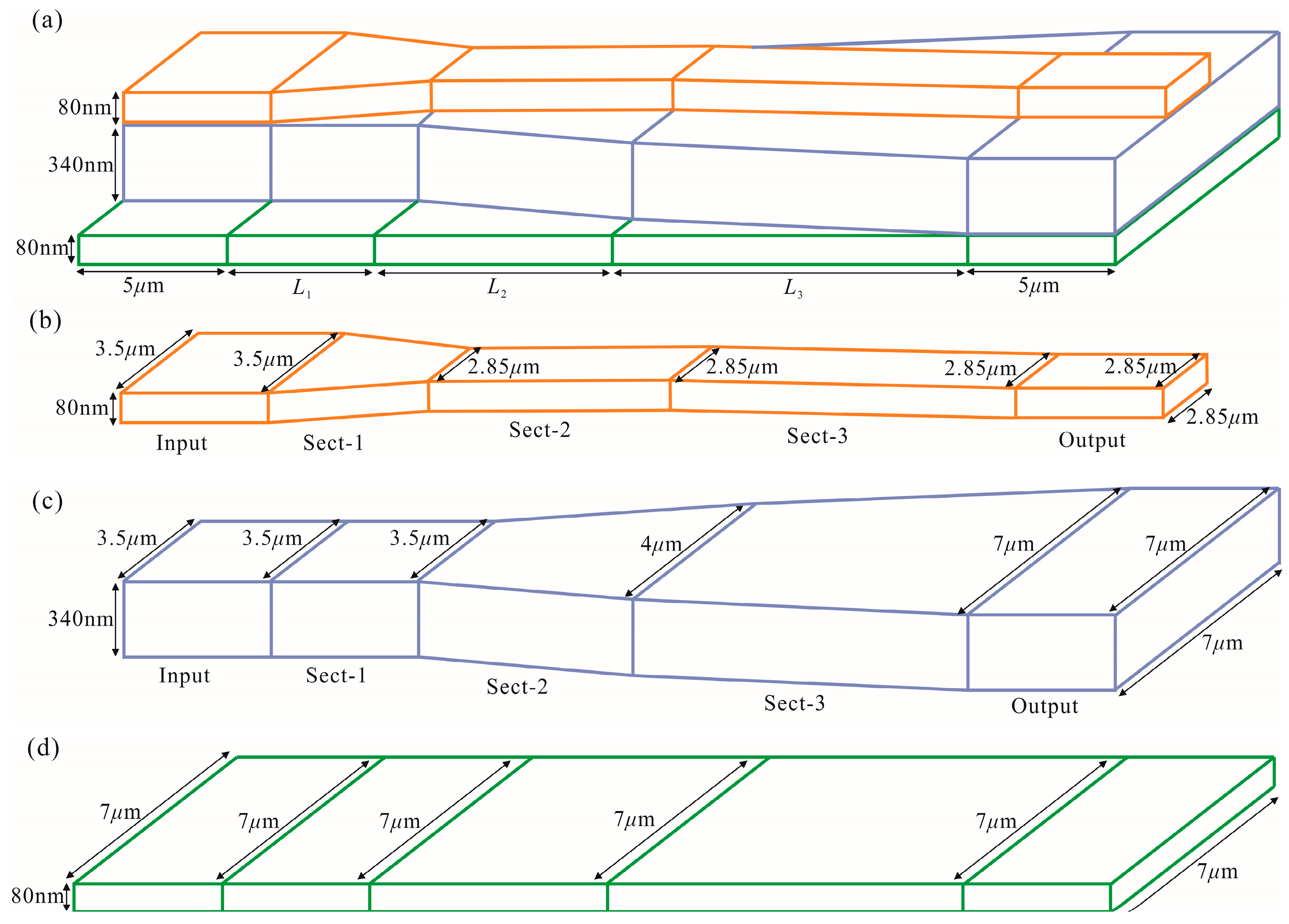
To explain the numerical method in detail, the case of an adiabatic device is presented in Figure 4, with wL = 3.50 μm and wR = 2.85 μm for the strongly guiding waveguide and the weakly guiding waveguide, respectively. The NAMSP method is carried out using a Lumerical Eigenmode Expansion (EME) solver [15]. The EME solver must add straight waveguides at both ends of the structure, as shown in Figure 4. The design here involves simultaneously tapering the widths of the two core layers, and this change in the width affects the mode both vertically and horizontally. The procedure for the NAMSP method is described in detail below.

3.1. The NAMSP Method

The steps of the NAMSP method are as follows.
First, the adiabatic device is designed in vertical and horizontal directions, respectively.
In the vertical direction, the DD scheme is implemented. The adiabatic device structure is divided into three subregions, where the top silicon taper waveguide changes from the width of 3.5 μm to that of 2.85, as shown in Figure 4b; the middle silicon taper waveguide changes from the width of 3.5 μm to that of 7 μm as shown in Figure 4c; and the width 7 μm of the bottom silicon planar waveguide remains unchanged, as shown in Figure 4d.
In the horizontal direction, the adiabatic device structure is divided into three sections: (a) Sect-1: w = 3.5 μm to w = 2.85 μm for the top silicon taper and W = 3.5 μm to W = 3.5 μm for the middle silicon taper; (b) Sect-2: w = 2.85 μm to w = 2.85 μm for the top silicon taper and W = 3.5 μm to W = 4 μm for the middle silicon taper; and (c) Sect-3: w = 2.85 μm to w = 2.85 μm for the top silicon taper and W = 4 μm to W = 7 μm for the middle silicon taper.
Second, for each section of the adiabatic device structure, a linear taper is used to join the input to the output. For Sect-1, the initial width of 3.5 μm is joined to the final width of 2.85 μm for the top silicon taper, and the initial width of 3.5 μm is joined to the final width of 3.5 μm for the middle silicon taper; both parts have a length of L1. For Sect-2, the initial width of 2.85 μm is joined to the final width of 2.85 μm for the top silicon taper, while the initial width of 3.5 μm is joined to the final width of 4 μm for the middle silicon taper, both with a length of L2. Finally, for Sect-3, the initial width of 2.85 μm is joined to the final width of 2.85 μm for the top silicon taper, and the initial width of 4 μm is joined to the final width of 7 μm for the middle silicon taper; each has a length of L3. Subsequently, we acquire the mode-connection power transfer efficiency (MCTE) [13] curve with TE0 mode at the input and output as a function of the length L, as shown in Figure 5. The MCTE is calculated using the “length scan” function in Lumerical EME simulator.
Third, we choose a value for the MCTE along the initial slope of the MCTE curve and determine the length for each section that corresponds to the desired mode-connection power loss fraction (MCLF) [13] value. Here, MCLF = 1 − MCTE, and we take MCLF = 0.0002 as an example. The lengths L1, L2, and L3 that correspond to MCLF = 0.0002 are 22.32 μm, 17.1 μm, and 34.0 μm, respectively, as shown in Figure 4.
Fourth, to construct each separate section, we use the section length L obtained in Step 3; subsequently, we combine all the sections to form the entire adiabatic device, as shown in Figure 6.
Fifth, to obtain the final MCTE curve, we scan the total length of the adiabatic device in its entirety, as plotted in Figure 7.
Sixth, to obtain the desired total length L for the adiabatic device, we use the final MCTE curve from the fifth step.
To perform a comparison of the adiabatic device with the straightforward NAMSP design, we use a linear-shape case for which the waveguide edges at input are joined to the waveguide edges at output via straight lines, as in the geometry shown in Figure 2. For comparison, the MCTE curve obtained for the linear-shape case is also plotted in Figure 7.
The figure shows the NAMSP case enables the same power transfer with a far shorter length than that of the linear-shape case. For example, at 99.9% power transfer, the required total length for the NAMSP case is 49 μm, whereas the linear-shape case requires a total length of 100 μm. Therefore, at 99.9% power transfer, the linear-shape case is more than twice as long as the NAMSP case. Hence, we have successfully shortened the adiabatic device using the NAMSP method and shown that the NAMSP-based design is more efficient than the linear-shape case design.

3.2. Operating Bandwidth of Adiabatic Devices Designed by NAMSP

To present the broad operating bandwidth of the adiabatic device designed using the NAMSP method, we plot the output MCTE curve in Figure 8 as a function of wavelength in the case when the total structural length is 68 μm. The figure shows the operating bandwidth defined by no more than 5% loss spans in the wavelength from 1050 nm (500 nm below the design wavelength of 1550 nm) to 4780 nm (3230 nm above the design wavelength of 1550 nm), which is an ultra-broad operating bandwidth.

3.3. Offset Adiabatic Device Designed by NAMSP

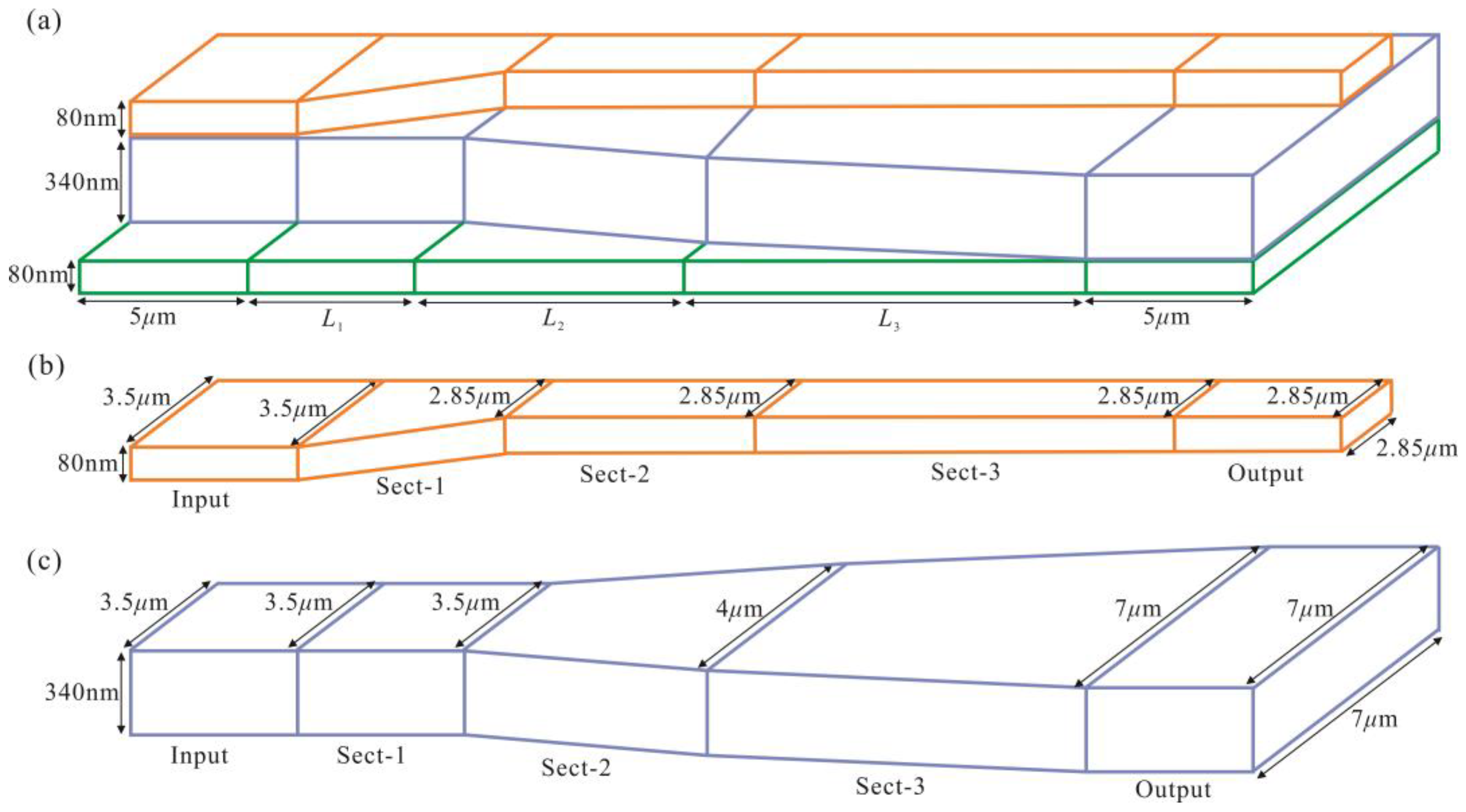
To illustrate how the NAMSP scheme can be applied to more complex devices, we illustrate the case of an offset adiabatic device. If one part or several parts of the ridge waveguide in PICs have an offset, the numerical method proposed herein can still be applied to the design. To show how the method can be applied in this case, we illustrate the case of an offset adiabatic device structure, wherein the weakly guiding waveguides have an offset, as shown in Figure 9.
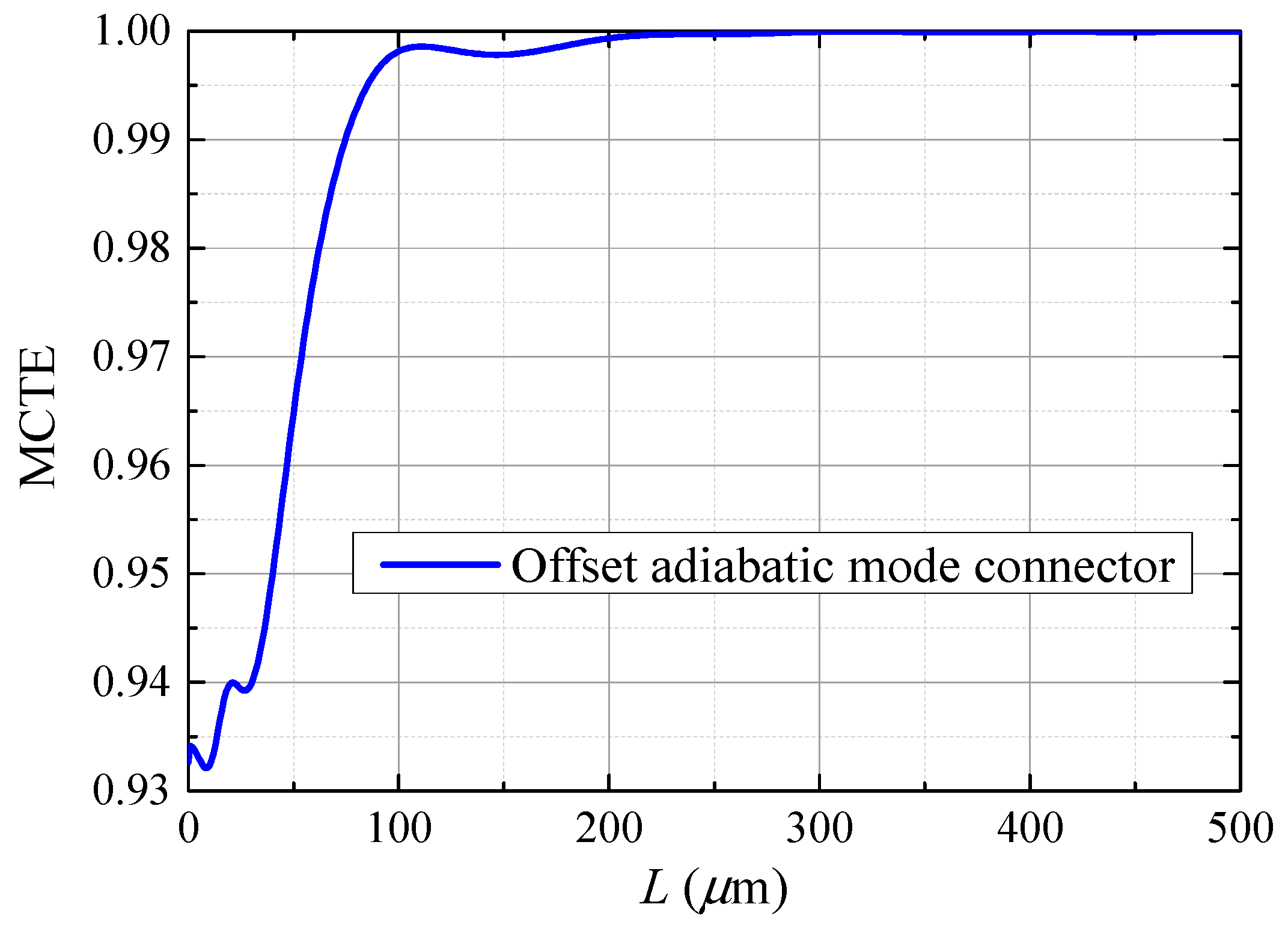
Using the NAMSP method, we can obtain the MCTE [15] curves for three different divided sections with TE1 mode at the input and output as a function of the section length Li, as shown in Figure 10. We choose a value for the MCTE along the initial slope and determine the length for each section that produces the desired MCLF value. Here, we take MCLF = 0.001 as an example. The lengths L1, L2, and L3 that correspond to MCLF = 0.001 are 67.71 μm, 40.40 μm, and 87.2 μm, respectively, as shown in Figure 9.
To construct each separate section, we use the obtained section length L; subsequently, we combine all the sections to form the entire adiabatic device. Finally, we scan the total length for the adiabatic device in its entirety to obtain the final MCTE curve, as plotted in Figure 11. For example, at 99.5% power transfer, the required total length for the NAMSP case is 85 μm, which is a short length for the offset adiabatic device.
Although this work focuses on the connection between the strongly guiding waveguide and the weakly guiding waveguide, the proposed numerical method is also applicable to the connection of other more complex waveguides. In such a case, the design procedure followed herein can be adopted: sectioning the 3D geometry and following the method to acquire the final shape.
When the width of the input waveguide is specified at the mode matching point, the resulting device length will be very compact. Further, when the input width is not 3.5 μm, the resulting device length will be greater than the length obtained at the mode matching point. This is the reason why the width of the input waveguide is specified at the mode matching point.

4. Conclusions

This study introduces the NAMSP method for designing an adiabatic device with multiple structural parameter variations. Furthermore, an efficient DD scheme is originally introduced into the NAMSP method. The design involves simultaneously tapering the width of two or more core layers. Since this change in the width affects the mode both vertically and horizontally, the numerical method proposed herein allows the shape of the width variation for each layer that enables an efficient adiabatic mode transformation to be obtained. The algorithm generates a more efficient guided-wave shape than that generated from the linear-shape case. The NAMSP-based adiabatic device design can also provide a broad operating bandwidth, thus verifying the efficiency and robustness of the proposed method. Refs. [12,13] are for the design of one structural parameter variation, while this study is for the design of multiple structural parameter variations. The DD scheme is particularly vital for the design of adiabatic devices with multiple structural parameter variations. Hence, the DD scheme is introduced into the proposed algorithm in this study. Therefore, the algorithm proposed in this study is also based on the constant power loss of the mode connection. However, the algorithm proposed by us is different from Refs. [12,13], regardless of the application scenario or the algorithm itself.
This study aims to describe the basic ideas and algorithms for the NAMSP method and demonstrate their basic validity. Such a numerical approach for designing efficient adiabatic devices has numerous applications in terms of designing devices in PICs and nano-photonics that seek the use of adiabatic mode evolution structure, which generally enables considerably broader operating optical bandwidths and a higher tolerance to fabrication variations compared to typical device structures, which are not based on the adiabatic mode evolution structure.

Author Contributions

Conceptualization, T.-L.L.; formal analysis, T.-L.L. and M.Y.; investigation, G.W. and J.S.; methodology, T.-L.L. and L.Z.; project administration, X.C.; writing—original draft, T.-L.L. and X.C.; writing—review and editing, T.-L.L., W.R. and W.S. All authors have read and agreed to the published version of the manuscript.

Funding

This work was partially supported by the National Natural Science Foundation of China (62161048, 62104117, 52101017, and 62201292), partially supported by Nantong Science and Technology Plan Project (JC2020138, JC12022087, JC2021030), and partially supported by Natural Science Research Project of Jiangsu Higher Education Institutions (22KJB140004).

Institutional Review Board Statement

Not applicable.

Informed Consent Statement

Not applicable.

Data Availability Statement

Not applicable.

Conflicts of Interest

The authors declare no conflict of interest.

References

  1. Tsuchizawa, T.; Yamada, K.; Fukuda, H.; Watanabe, T.; Takahashi, J.; Takahashi, M.; Shoji, T.; Tamechika, E.; Itabashi, S.; Morita, H. Microphotonics devices based on silicon microfabrication technology. IEEE J. Sel. Top. Quantum Electron. 2005, 11, 232–240. [Google Scholar]
  2. Manolatou, C.; Johnson, S.G.; Fan, S.; Villeneuve, P.R.; Haus, H.A.; Joannopoulos, J.D. High density integrated optics. J. Light. Technol. 1999, 17, 1682–1692. [Google Scholar] [CrossRef]
  3. Li, C.; Zhou, L.; Poon, A.W. Silicon microring carrier-injection-based modulators/switches with tunable extinction ratios and OR-logic switching by using waveguide cross-coupling. Opt. Express 2007, 15, 5069–5076. [Google Scholar] [CrossRef] [PubMed]
  4. Rong, H.; Jones, R.; Liu, A.; Cohen, O.; Hak, D.; Fang, A.; Paniccia, M. A continuous-wave Raman silicon laser. Nature 2005, 433, 725–728. [Google Scholar] [CrossRef] [PubMed]
  5. Barrios, C.A.; Almeida, V.R.; Panepucci, R.; Lipson, M. Electrooptic modulation of silicon-on-insulator submicrometer-size waveguide devices. J. Light. Technol. 2003, 21, 2332–2339. [Google Scholar] [CrossRef]
  6. Tang, Y.; Chen, H.-W.; Jain, S.; Peters, J.D.; Westergren, U.; Bowers, J.E. 50 Gb/s hybrid silicon traveling wave electro absorption modulator. Opt. Express 2011, 19, 5811–5816. [Google Scholar] [CrossRef] [PubMed]
  7. Dai, D.; Bowers, J.E. Novel concept for ultracompact polarization splitter-rotator based on silicon nanowires. Opt. Express 2011, 19, 10940–10949. [Google Scholar] [CrossRef] [PubMed]
  8. Dai, D.; Tang, Y.B.; Bowers, J.E. Mode conversion in tapered submicron silicon ridge optical waveguides. Opt. Express 2012, 20, 13425–13439. [Google Scholar] [CrossRef] [PubMed]
  9. Schmid, J.H.; Lamontagne, B.; Cheben, P.; Delage, A.; Janz, S.; Densmore, A.; Lapointe, J.; Post, E.; Waldron, P.; Xu, D.X. Mode converters for coupling to high aspect ratio silicon-on-insulator channel waveguides. IEEE Photonics Technol. Lett. 2007, 19, 855–857. [Google Scholar] [CrossRef]
  10. Aalto, T.; Solehmainen, K.; Harjanne, M.; Kapulainen, M.; Heimala, P. Low-loss converters between optical silicon waveguides of different sizes and types. IEEE Photonics Technol. Lett. 2006, 18, 709–711. [Google Scholar] [CrossRef]
  11. Dai, D.; He, J.; He, S. Elimination of multimode effects in a silicon-on-insulator etched diffraction grating demultiplexer with lateral tapered air slots. IEEE J. Sel. Top. Quantum Electron. 2005, 11, 439–443. [Google Scholar]
  12. Liang, T.L.; Tu, Y.; Chen, X.; Huang, Y.; Bai, Q.; Zhao, Y.; Zhang, J.; Yuan, Y.; Li, J.; Yi, F.; et al. A Fully Numerical Method for Designing Efficient Adiabatic Mode Evolution Structures (Adiabatic Taper, Coupler, Splitter, Mode Converter) Applicable to Complex Geometries. J. Lightw. Technol. 2021, 39, 5531–5547. [Google Scholar] [CrossRef]
  13. Liang, T.L.; Cheng, X.; Yu, M.; Zhang, L.; Shi, J.; Shao, W. Numerical method for designing ultrashort and efficient adiabatic mode converters. J. Opt. Soc. Am. B 2022, 39, 2637–2642. [Google Scholar] [CrossRef]
  14. Lumerical Solutions. FDTD Solutions. 2018. Available online: https://www.lumerical.com (accessed on 13 September 2020).
  15. Lumerical Solutions. Mode Solutions. 2018. Available online: https://www.lumerical.com (accessed on 22 September 2020).
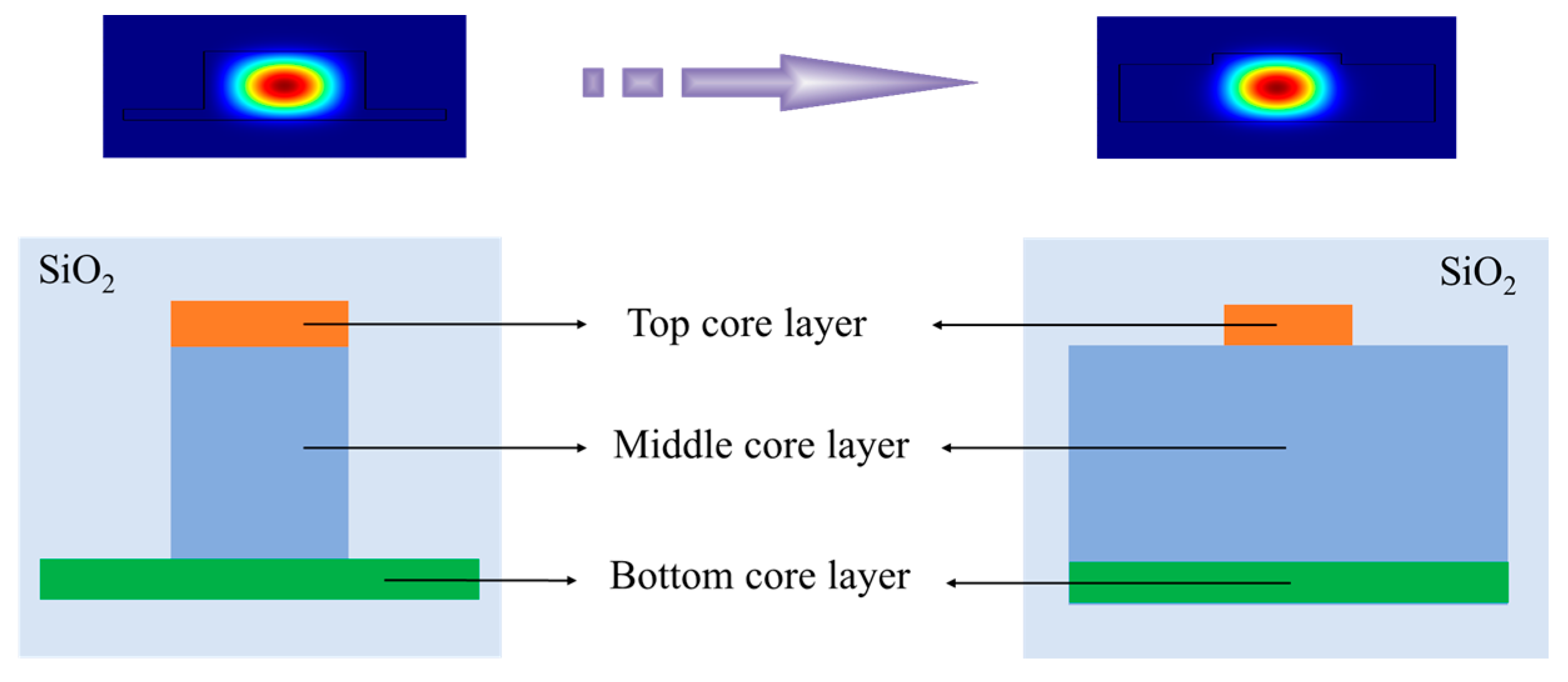
Figure 1. Two ridge waveguides. The insets show the TE fundamental mode shapes for different waveguides.
Photonics 10 00517 g001
Figure 2. Ridge waveguide structures. The inset shows a linear shape design of the adiabatic device connects.
Photonics 10 00517 g002
Figure 3. The trends of neff and cH variation with width wL in the strongly guiding waveguide.
Photonics 10 00517 g003
Figure 4. (a) The 3D view of designed adiabatic device. (b) The layout of the top silicon taper waveguide. (c) The layout of the middle silicon taper waveguide. (d) The bottom silicon planar waveguide.
Photonics 10 00517 g004
Figure 5. MCTE curves vs. length L for the three sections of the device structure: (a) Sect-1; (b) Sect-2; and (c) Sect-3.
Photonics 10 00517 g005
Figure 6. The 3D geometrical shape of the adiabatic device for the NAMSP method.
Photonics 10 00517 g006
Figure 7. MCTE curve for the adiabatic device structure designed by NAMSP; the MCTE curve for the linear-shape case is shown for comparison.
Photonics 10 00517 g007
Figure 8. Operation bandwidth of the adiabatic device for the NAMSP case with a total structural length of 68 μm.
Photonics 10 00517 g008
Figure 9. (a) The 3D view of designed offset adiabatic device. (b) The layout of the top silicon taper waveguide. (c) The layout of the middle silicon taper waveguide.
Photonics 10 00517 g009
Figure 10. MCTE curves vs. length L for the three different divided sections of the offset adiabatic device structure: (a) Sect-1; (b) Sect-2; and (c) Sect-3.
Photonics 10 00517 g010
Figure 11. MCTE curve for the offset adiabatic device structure obtained via the NAMSP method.
Photonics 10 00517 g011
Table 1. Related Parameters for Different Width wL.
TypewL/μmneffcH/nmcV/nm
Weakly guiding waveguide2.853.2738996192
Strongly guiding waveguide3.403.2734965192
3.453.2737979192
3.483.2737987192
3.503.2738993192
3.523.2740999192
3.553.27411007192
Disclaimer/Publisher’s Note: The statements, opinions and data contained in all publications are solely those of the individual author(s) and contributor(s) and not of MDPI and/or the editor(s). MDPI and/or the editor(s) disclaim responsibility for any injury to people or property resulting from any ideas, methods, instructions or products referred to in the content.