Abstract
Transmission spectra of a symmetric microresonator structure, with dielectric Bragg mirrors, are obtained. The working cavity of the structure is partially filled by a layer of a quarter-wave thickness of finely layered “graphene–semiconductor” medium, with material parameters controlled by external electric and magnetic fields. It is shown, that the transformation of the spectra is achieved both by changing the energy state of the graphene layers and by changing the external magnetic field. The spectral characteristics for the inverted and doped states of graphene layers are established.
1. Introduction
Photonic crystal microresonators (MCRs) have attracted the close attention of researchers in recent years, largely due to their wide use in various optical devices [1,2,3,4,5,6,7,8,9]. One of the important research directions, is the selective extraction and amplification of an optical signal, based on the interaction of optical modes in a microresonator and resonances in the active medium filling its cavity. For many practical applications, it is important to be able to tune the resonant frequency of a microresonator, by changing the external parameters. Efficient rearrangement of the transmission and reflection spectra of a microresonator, can be achieved by introducing a medium into the cavity between the mirrors, the material parameters of which depend on easily changed external factors [9,10]. The use of resonant photonic crystals, in which the interaction of optical and, for example, exciton resonances, requires the correct selection of both geometry and materials for the Bragg mirrors (BMs) and cavity.
One-dimensional MCRs, represent a structure in which, as a rule, plane layered dielectric Bragg reflectors are used as mirrors. The formation of a symmetric MCR requires two identical dielectric Bragg mirrors separated from each other by a certain distance along their axis, and a symmetrical order of the layers relative to the cavity in one of the BMs. The area between the mirrors (the working cavity), as a rule, is filled with an active medium. Due to the multiple reflection of radiation between the mirrors, standing waves (resonator modes) are formed. In plane-parallel resonators, only those modes are supported for which the distance between the mirrors is a multiple of half the wavelength of the propagating radiation. In this case, transmission resonances are observed in the photonic band gaps (PBGs). Their number, position, and amplitude are determined by the width of the cavity and the reflection coefficient of the mirrors.
Rearrangement of the resonant frequency of a microresonator by changing external parameters, is an important possibility for many practical applications [11,12,13,14]. Efficient rearrangement of the transmission and reflection spectra of a microresonator can be achieved, by introducing into the cavity between the mirrors a medium whose material parameters depend on easily changed external factors [15,16,17,18,19,20]. One of the most promising materials for photonics is graphene, and various planar structures based on it. Graphene can be in both passive and active (doped or inverted) states. We will call graphene doped if it is in an equilibrium state with a nonzero chemical potential (Fermi energy), and we will call it inverted if it is in a nonequilibrium state, i.e., in the presence of an inverse band population. Graphene’s parameters can be controlled by changing its chemical potential (Fermi energy) [21,22,23,24,25,26,27,28].
Thus, the above features of graphene-containing structures, make it possible to design tunable multichannel filters with the desired number of channels and ultra-narrow bands, in such a structure [29]. A graphene-containing photonic crystal can be used as a miniature biosensor for cancer cell recognition [30]. The presence of an effective graphene medium in the microcavity structure, can lead to partial or complete suppression of the defect mode, as well as to a significant dependence of the character of the spectra on the energy state of the graphene. Variation of the Fermi energy (quasi-energy), makes it possible not only to rearrange the photon spectra, by changing the reflection, transmission, and absorption of the radiation incident on the structure over a wide range, but also to create conditions for amplifying the radiation interacting with the structure [31].
In this paper, we study the features of the transmission spectra of a symmetric microresonator with dielectric BMs, in the working cavity of which, a layer of a quarter-wave thickness of finely layered “semiconductor–graphene” medium, with material parameters controlled by external electric and magnetic fields, is placed. It is proposed to use it as a material for semiconductor layers . The paper presents the frequency dependences of the transmission coefficient of the eigen-TM wave at different static magnetic fields and different types of excitation of the graphene layers, as well as different order of the layers in the BMs.
2. Material Parameters of the Structure
Let us consider a symmetrical microresonator formed by two BMs, and a cavity separating them. We assume that the period of the BMs consists of two layers of isotropic dielectrics, these are and , with permittivity and , respectively, and the same optical thicknesses . Here, , where the operating frequency is . The real thicknesses of the layers are and , the period is , and the number of periods in each of the BMs is . The transverse dimensions of the layers must be much greater than the operating wavelength , and also be greater than the transverse dimension of the optical beam introduced into the microresonator (as a rule, these dimensions are several millimeters). The cavity has a length and a permittivity . Let us first consider the distribution of the wave field over the structure with an unfilled cavity, in order to reveal the spectral features of the microcavity that arise when the cavity is filled with an effective medium.
Figure 1 shows the distribution of the permittivity along the structure (layer interfaces are perpendicular to the OZ axis), and the squared modulus of the electric field strength of the wave for the resonator structure under consideration (thin and thick lines, respectively), obtained with two orderings of layers in the BMs: (hereafter referred to as structure D), and (hereafter referred to as structure F). The distribution of the electric field corresponds to the frequency , and the permittivity of the cavity and . It can be seen that the amplitude of the electric field reaches a maximum at the center of the cavity for structure D (the cavity is limited by layers with a higher permittivity), and is minimal at the lateral boundaries (in this case, the magnetic field amplitude at the center of the cavity is minimal, and at its boundaries it is a maximum). The cavity is bounded by layers with a low dielectric permittivity in the BMs, for a structure with a changed order of the layers, while the electric field amplitude is minimal in the center and maximal at the lateral boundaries of the cavity, for a magnetic field, the amplitude is maximum in the center and minimal at the cavity boundaries.
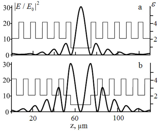
Figure 1.
The distribution of the modulus of the electric field strength of the wave and the permittivity (thick and thin lines, respectively) in a microresonator, with a cavity thickness and , at , . (a) structure D-type, , ; (b) structure F-type.
The transfer matrix connecting the wave field at the input and output of the structure, for a microresonator with a free resonator cavity, has the form (the view of the transfer matrices of individual layers is presented in Section 3). The transmission spectra of the considered structures are shown in Figure 2. There is a photonic band gap (PBG) in the operating frequency region, which is wider for the D structure than for the F structure. The defect mode is a narrow peak of almost complete transmission, associated with a violation of the periodicity of the structure; it is observed in the center of the forbidden region in both cases.
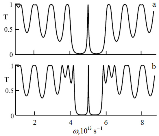
Figure 2.
Frequency transmission spectra of a microresonator, with a cavity thickness and , at , . (a) structure D-type, , ; (b) structure F-type.
Let us estimate the value of the quality factor of the resonant structure under study. To do this, we use the definition that relates the value of the resonant frequency to the width of the resonant curve at its half-height, i.e., [32]. Using the above spectra to determine the width of the central mode curve for the two types of structures, we obtain: and . Thus, for the same number of periods in the BMs, the quality factor of the resonator depends on the order of the layers in them. The quality factor of the microresonator increases with an increase in the number of periods in the BMs and the optical contrast in neighboring layers of the mirror period.
Next, we will fill the cavity with an active plane-layered structure, composed of alternating layers of semiconductor and graphene, with thicknesses and . The material parameters of each layer in the studied frequency range are scalar-tensor quantities, i.e., for graphene and the semiconductor, and , the magnetic permeability of the layers in the studied range can be considered to be equal to unity. Such a one-dimensional structure, even in the absence of an external magnetic field, has the properties of a uniaxial crystal, with a symmetry axis perpendicular to the interfaces between the layers (axis ).
An external static magnetic field applied in the layer plane, leads to the anisotropy of the optical properties of the semiconductor layers. For a field oriented along the axis, the nonzero components of the semiconductor permittivity tensor , , depend on the frequency and the external magnetic field, as follows [33]:
where the plasma and cyclotron frequencies of the semiconductor are introduced: and , is the lattice part of the permittivity, e is the electron charge, and are the concentration and the effective mass of the carriers, respectively, , is the relaxation parameter. Resonance absorption in the semiconductor layer is realized at a frequency for the above orientation of the magnetic field and transverse (with respect to ) propagation of an electromagnetic wave.
A planar magnetic field does not affect the electronic subsystem of graphene, due to its geometry, i.e., monolayer. In this case, the effective permittivity tensor of the finely layered graphene medium, has nonzero components: , . The eigenwaves of the effective medium in the case of transverse propagation of the wave (), are and waves. We will carry out further analysis for a -type wave, because this type of wave is controlled by an external magnetic field. The propagation constant of this wave is . Where , and is the effective permittivity for the considered problem geometry. In the long-wave approximation (), the effective permittivity can be represented as
where , and the parameter . When writing , it was taken into account that for graphene, the permittivity is related to its surface conductivity by the relation . In real structures, (since nm) and the parameter .
Graphene layers can be in both unexcited and active states. In unexcited graphene, the Fermi energy (chemical potential) is at the Dirac point, and is equal to zero. In this case, the valence band is completely filled, the conduction band is completely free, and the band gap is absent. The chemical potential can be shifted to the conduction band or the valence band, the charge density on the graphene sheet can be changed, and thus the surface conductivity can be changed by applying a voltage of different polarity between the graphene sheet and the substrate.
Doped and inverted graphene are distinguished, for which the filling of the conduction and valence bands is different, and the expressions for surface conductivity are different. The frequency dependences of the dynamic surface conductivity of doped and inverted graphene, within the framework of the Kubo model, are determined, respectively, by the following expressions [34,35]:
Here, is the fundamental (static) conductivity of graphene, e is the charge of an electron, ℏ is Planck’s constant, is the Boltzmann constant, T is the temperature, is the carrier scattering time, and is the Fermi energy (for doped graphene) and the quasi-Fermi energy (for inverted graphene). Both expressions at , lead to the same dependence for passive (i.e., unexcited) graphene.
Figure 3a,b show the frequency dependence of the real part of the conductivity of inverted and doped graphene, obtained at K, ps (hereafter) and values of the Fermi energy (quasi-energy) , 50, 100, 150, and 200 meV (curves 1–5). It can be seen that the real part of the conductivity for doped graphene, takes only positive values in the entire frequency range and for all values of the Fermi energy, while negative values are realized for inverted graphene in the frequency range THz. The imaginary part of the conductivity, according to (3), remains positive over the entire frequency range and has a monotonically decreasing character of the hyperbolic type for both types of graphene.
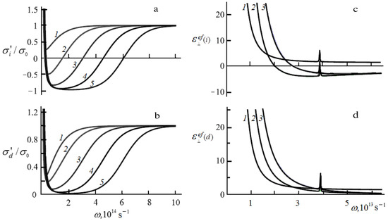
Figure 3.
Frequency dependence of the real part of the conductivity of inverted and doped graphene (a,b) for , 50, 100, 150, and 200 meV (curves 1–5); and frequency dependence of the imaginary part of the medium’s effective permittivity for inverted and doped graphene (c,d) for kOe, , 100, and 200 meV (curves 1–3).
Figure 3c,d show the frequency dependences of the imaginary part of the effective permittivity of a finely layered medium with inverted and doped graphene, obtained for the parameters , , is the mass of a free electron, (hereafter), , 100, 200 meV (curves 1–3), and kOe. A significant dependence of this value on the degree of excitation of graphene is visible, i.e., dependence of the value on the Fermi energy (quasi-energy). It is important that for inverted graphene, at frequencies where the real part of the conductivity is negative, the imaginary part of the effective permittivity is also negative. In this region, an increase in the waves transmitted and reflected from the structure should be observed; with increasing quasi-Fermi energy, this region expands significantly. In a narrow region near the frequency , a resonant increase in the imaginary part of the effective permittivity of a fine-layered medium is observed. Increasing the magnetic field, shifts the resonance peak to higher frequencies and increases the amplitude of the resonance peak. Thus, the effective permittivity of the layer filling the resonant cavity of the microresonator, can be controlled using both electric and magnetic fields.
3. Microresonator Spectra with a Partially Filled Cavity
Let us consider the transformation of the transmission spectrum of a TM wave when a layer of an effective medium is placed in the center of the microresonator cavity. For a microresonator structure with a resonator cavity partially filled with an effective medium, the transfer matrix connecting the wave field at the input and output of the structure has the form . The transfer matrices of individual layers, written in the plane wave approximation (valid for the above transverse dimensions of the layers), have the form [19,33]:
where , are the propagation constants in the respective layers, , and c are the frequency and speed of the wave in a vacuum, respectively, .
The amplitude transmission and reflection coefficients for the entire microresonator structure, are determined in terms of the matrix elements of the transfer matrix [19,35]:
The energy transmission and reflection coefficients, in the case of a symmetrical environment (we assume that the structure is in a vacuum), have the form , . When absorption in layers is taken into account, the fraction of energy absorbed by the structure is determined by the quantity . This relation is valid for equilibrium states; therefore, its use for inverted graphene is incorrect.
The character of the spectra essentially depends on both the energy state of graphene in a finely layered medium and the magnitude of the applied magnetic field. Figure 4 shows the frequency dependence of the transmittance T, for a microresonator with different layer order in BMs (D, F− a, b) and a partially filled cavity. We assume that a layer of an effective medium, with a thickness (in this case when ), with unexcited graphene (), is placed in the center of the cavity. We note that the difference between the spectra , for structures with a different order of layers in BMs, manifests itself in the position of resonance lines inside the photonic band gap and in the form of the spectrum envelope outside the band gap. With increasing field strength, these changes in the spectra become more noticeable. This is due to the fact that the optical thickness of the insert from the effective medium , in the process of tuning, is not constant, but depends not only on the frequency, but also on the external field. Consequently, the phase-matching conditions and, accordingly, the character of the spectrum, also depend on the field. It can be seen from the spectral dependences shown in series , that when the layer of the effective medium is placed at the maximum of the electric wave field, already at , the resonant line of the microresonator with an empty cavity (dashed line) is partially suppressed, and shifted to the low-frequency region. At the side peak at the low-frequency boundary of the photonic band gap, splitting occurs. The shift of the defective mode to the region of higher frequencies, as well as a separate splitting of the peak from the low-frequency part of the spectrum and its shift to the high-frequency region, is observed with increasing magnetic field.
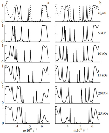
Figure 4.
Frequency dependence of the transmittance, for a microresonator, with a D-type (a) and F-type (b) insert, for meV.
When the layer of the effective medium is placed in the minimum of the electric field (b), a similar transformation of the spectrum occurs, however, the quantitative character of the transformation differs from case (a). The main difference, lies in the significant rearrangement of the spectrum at the high-frequency boundary of the photonic band gap, where, already at , two sharp peaks are split off from the high-frequency boundary of the band gap and shifted to lower frequencies. The separate splitting of the peak from the low-frequency part of the spectrum, and its shift to the high-frequency region, occurs with increasing magnetic field, along with a shift of these peaks. As the field increases further, their significant suppression is observed. The transmittance cannot exceed unity for a microcavity with an insert containing unexcited graphene.
An analysis of the obtained spectra, shows that their transformation for the D and F structures, although it has quantitative differences, is qualitatively similar, therefore, below we consider only the spectra for the D-type structure (with the order of the layers in the BMs ). Figure 5 shows the transmission spectra for a microcavity structure corresponding to inverted (a) and doped (b) graphene, with excited graphene layers ( meV), in an effective medium. Note the change in the character of the transmission spectra in the case of excited and unexcited graphene. First of all, such changes are associated with the appearance of amplification in the spectrum of a microresonator with an inverted graphene insert. In this case, the amplification at the frequency of the defective mode, is much greater than that away from it. A significant dependence of the structure’s transmittance on the external magnetic field is also seen. As the field increases, additional peaks appear in the photonic bandgap, which are shifted to the high-frequency region.
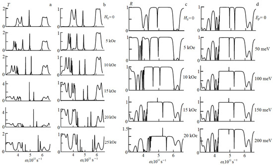
Figure 5.
Frequency dependence of the microresonator transmittance, with a D-type insert, with inverted and doped (a,b) graphene, for meV; and frequency dependence of the microresonator reflection coefficient with a D-type insert, with inverted graphene, for meV (c) and kOe (d).
Along with the rearrangement of the transmission spectrum, under the influence of a magnetic field and a change in the excitation energy of graphene, the reflection and absorption spectra are also rearranged. Figure 5 shows the reflection spectra for a microcavity with a D-type insert with inverted graphene, in the case of two control modes: at a fixed value meV and various values of the magnetic field (c), and also at a fixed value of the field kOe and various values (d). The transformation of the spectra, and the presence of amplification for the structure with inverted graphene, are visible for both control modes. Note that the appearance of narrow peaks with , takes place at the same frequencies, where , however, not all values correspond to an excess of unity by the reflection coefficient. If does not exceed unity by much, then the coefficient does not exceed unity.
Figure 6 shows the reflection and absorption spectra for a type D microcavity structure with doped graphene, constructed on the basis of relations (5), and corresponding to the Fermi energy meV and two field values kOe. As expected, in this case, the law of conservation of energy is satisfied at all frequencies, and does not exceed unity. The absence of reflection, and weak absorption , are observed near the operating frequency (at the center of the PBG) and at the low-frequency edge of the zone, in the absence of an external field. The presence of the field leads to a change in the reflection and absorption coefficients in the low-frequency region. In particular, a frequency appears in the interval , at which there is no reflection, and the absorption reaches the value . In the high-frequency region, absorption is also practically absent.
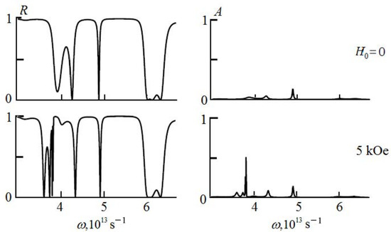
Figure 6.
Frequency dependence of the microresonator reflection and absorption coefficients, with a D-type insert, with doped graphene, for meV.
4. Discussion
Achievements in computer technology, make it possible to carry out numerical experiments without expensive costs for the production and obtaining of materials, by investigating and selecting the structure parameters for specific tasks. In this paper, when describing the parameters of a fine-layered “semiconductor–graphene” medium, we use indium antimonide, with an electronic type of conductivity, as a semiconductor. It has the highest electron mobility (about 78,000 cm) and the longest electron free path (up to at 300 K) among all known semiconductor materials. Modern technologies make it possible to form photonic crystals based on , with specified geometric and physical parameters. Graphene in the active state, can be obtained using optical or current (electrical) pumping [36,37,38]. The approximation of an effective medium (or fine-layered), can be used under the condition . In our case, the operating wavelength of the radiation is , and the total thickness of the active layer in our case is . Assuming the number of periods in the “semiconductor–graphene” structure to be equal to , we arrive at the period of the structure being , which indicates the correctness of using the approximation of a finely layered medium. Note that we have not considered the transformation of the spectra, which is possible when the doping of the semiconductor is changed. However, the given expressions for the semiconductor permittivity components take into account changes in the material parameters, which can be taken into account in calculations based on the given relationships.
5. Conclusions
This paper presents the frequency dependences of the transmission, reflection, and absorption coefficients for a wave propagating in a symmetric microresonator structure with dielectric BMs. The working cavity of the resonator is partially filled with an active layer of a quarter-wave thickness, which is a periodic “graphene–semiconductor” structure, with controlled material parameters of individual layers. It is shown that the transformation of the spectra can be achieved both by changing the chemical potential of graphene layers and its conductivity, under the action of an external electric field, and by changing the dielectric constant of the semiconductor layers under the action of an external magnetic field.
The approximation of an effective (fine-layered) medium is used in modeling the photon spectra of a microcavity structure, to describe the optical properties of the active layer. The operating frequency range of the microresonator from the terahertz to the optical region, can be changed by choosing the material of the semiconductor layers, their thickness, type, and concentration of carriers, as well as by choosing the period of the BMs. The creation of amplification in graphene layers largely depends on the possibility of maintaining a long-lived inverse population on them, with the help of optical pumping. The character of the spectra for a microresonator structure, in which the active material contains layers of graphene in an inverted and doped state, has been established.
Author Contributions
Conceptualization, D.I.S.; methodology, S.V.E. and I.V.F.; software, S.V.E. and I.V.F.; formal analysis, S.V.E. and I.V.F.; investigation, S.V.E., I.V.F., and D.I.S.; resources, D.I.S.; data curation, S.V.E. and I.V.F.; writing—original draft preparation, I.V.F. and D.I.S.; writing—review and editing, S.V.E.; supervision, D.I.S.; project administration, D.I.S. All authors have read and agreed to the published version of the manuscript.
Funding
This research received no funding.
Institutional Review Board Statement
Not applicable.
Informed Consent Statement
Not applicable.
Data Availability Statement
Not applicable.
Conflicts of Interest
The authors declare no conflict of interest. The funders had no role in the design of the study, in the collection, analyses, or interpretation of data, in the writing of the manuscript, or in the decision to publish the results.
Abbreviations
The following abbreviations are used in this manuscript:
| MCRs | Microresonators |
| BMs | Bragg mirrors |
| PBGs | Photonic band gaps |
References
- Heebner, J.; Grover, R.; Ibrahim, T. Optical Microresonator Theory, Fabrication, and Applications; Springer: New York, NY, USA, 2008; p. 268. [Google Scholar]
- Hodgson, N.; Weber, H. Optical Resonators: Fundamentals, Advanced Concepts, Applications; Springer Science & Business Media: New York, NY, USA, 2005; p. 795. [Google Scholar]
- Matsko, A.B. Practical Applications of Microresonators in Optics and Photonics; CRC Press: New York, NY, USA, 2018; p. 586. [Google Scholar]
- Eliseeva, S.V.; Fedorova, I.V.; Sementsov, D.I. Photon Spectra of a Bragg Microresonator with Bigyrotropic Filling. Photonics 2022, 9, 391. [Google Scholar] [CrossRef]
- Mohebbi, M. Refractive index sensing of gases based on a one-dimensional photonic crystal nanocavity. J. Sensors Sens. Syst. 2015, 4, 209–215. [Google Scholar] [CrossRef]
- Fedorova, I.V.; Eliseeva, S.V.; Sementsov, D.I. Photonic spectra of a Bragg microresonator with a ferroelectric resonator layer. Superlattices Microstruct. 2018, 117, 488–494. [Google Scholar] [CrossRef]
- Bayindir, M.; Kural, C.; Ozbay, E. Coupled optical microcavities in one-dimensional photonic bandgap structures. J. Opt. Pure Appl. Opt. 2001, 3, S184. [Google Scholar] [CrossRef]
- Lei, F.; Ward, J.M.; Romagnoli, P.; Chormaic, S.N. Polarization-controlled cavity input-output relations. Phys. Rev. Lett. 2020, 124, 103902. [Google Scholar] [CrossRef] [PubMed]
- Chremmos, I.; Schwelb, O.; Uzunoglu, N. Photonic Microresonator Research and Applications; Springer: New York, NY, USA, 2010; p. 530. [Google Scholar]
- Kumar, V.; Suthar, B.; Malik, J.; Kumar, A.; Singh, K.S.; Singh, T.; Bhargva, A. Defect mode properties and origin in one dimensional photonic crystal. Photonics Optoelectron. 2013, 2, 19–25. [Google Scholar]
- Sadegzadeh, S.; Mousavi, A. A Comparative Study of a Defective Superconductor/Semiconductor-Dielectric Photonic Crystal. Int. J. Phys. Math. Sci. 2017, 11, 247–250. [Google Scholar]
- AL-Zahrani, H.A.M. Simulation and design of photonic crystal with nonlinear components. Sciences 2018, 8, 690–704. [Google Scholar]
- Eliseeva, S.; Sannikov, D.; Sementsov, D. Anisotropy, gyrotropy and dispersion properties of the periodical thin-layer structure of magnetic–semiconductor. J. Magn. Magn. Mater. 2010, 322, 3807–3816. [Google Scholar] [CrossRef]
- Tarapov, S.; Belozorov, D. Microwaves in dispersive magnetic composite media. Low Temp. Phys. 2012, 38, 603–625. [Google Scholar] [CrossRef]
- Arkhipkin, V.; Gunyakov, V.; Myslivets, S.; Gerasimov, V.; Zyryanov, V.Y.; Vetrov, S.Y.; Shabanov, V. One-dimensional photonic crystals with a planar oriented nematic layer: Temperature and angular dependence of the spectra of defect modes. J. Exp. Theor. Phys. 2008, 106, 388–398. [Google Scholar] [CrossRef]
- Eliseeva, S.; Sementsov, D. Defect modes and magnetooptical activity of a one-dimensional magnetophotonic crystal. J. Exp. Theor. Phys. 2011, 112, 199–203. [Google Scholar] [CrossRef]
- Tang, R.Y.; Wu, J.W.; Nakarmi, B. Investigation of band-gap properties in one-dimensional ternary photonic crystals with a single defect layer. Quantum Electron. 2016, 46, 640. [Google Scholar] [CrossRef]
- Vetrov, S.Y.; Avdeeva, A.Y.; Timofeev, I. Spectral properties of a one-dimensional photonic crystal with a resonant defect nanocomposite layer. J. Exp. Theor. Phys. 2011, 113, 755–761. [Google Scholar] [CrossRef]
- Eliseeva, S.; Sementsov, D. Optical spectra of one-dimensional defect photonic crystals. Opt. Spectrosc. 2010, 109, 729. [Google Scholar] [CrossRef]
- Hu, C.A.; Liu, J.W.; Wu, C.J.; Yang, T.J.; Yang, S.L. Effects of superconducting film on the defect mode in dielectric photonic crystal heterostructure. Solid State Commun. 2013, 157, 54–57. [Google Scholar] [CrossRef]
- Averkov, Y.O.; Yakovenko, V.; Yampol’Skii, V.; Nori, F. Terahertz transverse-electric- and transverse-magnetic-polarized waves localized on graphene in photonic crystals. Phys. Rev. B 2014, 90, 045415. [Google Scholar] [CrossRef]
- Evseev, D.A.; Eliseeva, S.V.; Sementsov, D.I.; Shutyi, A.M. A Surface Plasmon–Polariton in a Symmetric Dielectric Waveguide with Active Graphene Plates. Photonics 2022, 9, 587. [Google Scholar] [CrossRef]
- Razi, S.; Ghasemi, F. Tunable graphene based one dimensional photonic crystal with applications in terahertz optical integrated circuits. Phys. B Condens. Matter 2019, 566, 77–85. [Google Scholar] [CrossRef]
- Mahmoodzadeh, H.; Rezaei, B. Tunable Bragg defect mode in one-dimensional photonic crystal containing a graphene-embedded defect layer. Appl. Opt. 2018, 57, 2172–2176. [Google Scholar] [CrossRef]
- Morozov, S.V.; Novoselov, K.S.; Geim, A.K. Electron transport in graphene. Physics-Uspekhi 2008, 51, 744–748. [Google Scholar] [CrossRef]
- Falkovsky, L.A. Optical properties of graphene and IV–VI semiconductors. Physics-Uspekhi 2008, 51, 887. [Google Scholar] [CrossRef]
- Aleshkin, V.Y.; Dubinov, A.A.; Ryzhii, V. Terahertz laser based on optically pumped graphene: Model and feasibility of realization. Jetp Lett. 2009, 89, 63–67. [Google Scholar] [CrossRef]
- Morozov, M.Y.; Moiseenko, I.; Popov, V. Giant amplification of terahertz plasmons in a double-layer graphene. J. Phys. Condens. Matter 2018, 30, 08LT02. [Google Scholar] [CrossRef]
- Belhadj, W.; Al-Ahmadi, A.N. Tunable narrowband terahertz multichannel filter based on one-dimensional graphene-dielectric photonic crystal. Opt. Quantum Electron. 2021, 53, 1–17. [Google Scholar] [CrossRef]
- Panda, A.; Pukhrambam, P.D.; Wu, F.; Belhadj, W. Graphene-based 1D defective photonic crystal biosensor for real-time detection of cancer cells. Eur. Phys. J. Plus 2021, 136, 809. [Google Scholar] [CrossRef]
- Eliseeva, S.; Sementsov, D. Spectra of a Bragg Microcavity with an Active Graphene Medium. Bull. Russ. Acad. Sci. Phys. 2022, 86, 1144–1150. [Google Scholar] [CrossRef]
- Faneca, J.; Perova, T.S.; Tolmachev, V.; Baldycheva, A. One-dimensional multi-channel photonic crystal resonators based on silicon-on-insulator with high quality factor. Front. Phys. 2018, 6, 33. [Google Scholar] [CrossRef]
- Bass, F.G.; Bulgakov, A.A.; Tetervov, A.P. High-Frequency Properties of Semiconductors with Superlattices; Nauka: Moscow, Russia, 1989; p. 288. [Google Scholar]
- Gurevich, A.G.; Melkov, G.A. Magnetization Oscillations and Waves; CRC Press: Boca Raton, FL, USA, 2020; p. 464. [Google Scholar]
- Born, M.; Wolf, E. Principles of Optics: Electromagnetic Theory of Propagation, Interference and Diffraction of Light; Cambridge University Press: Cambridge, UK, 1999; p. 952. [Google Scholar]
- Clark, G.; Schaibley, J.R.; Ross, J.; Taniguchi, T.; Watanabe, K.; Hendrickson, J.R.; Mou, S.; Yao, W.; Xu, X. Single defect light-emitting diode in a van der Waals heterostructure. Nano Lett. 2016, 16, 3944–3948. [Google Scholar] [CrossRef]
- Brem, S.; Wendler, F.; Winnerl, S.; Malic, E. Electrically pumped graphene-based Landau-level laser. Phys. Rev. Mater. 2018, 2, 034002. [Google Scholar] [CrossRef]
- Ryzhii, V.; Otsuji, T.; Ryzhii, M.; Aleshkin, V.Y.; Dubinov, A.; Svintsov, D.; Mitin, V.; Shur, M. Graphene vertical cascade interband terahertz and infrared photodetectors. 2D Mater. 2015, 2, 025002. [Google Scholar] [CrossRef]


Disclaimer/Publisher’s Note: The statements, opinions and data contained in all publications are solely those of the individual author(s) and contributor(s) and not of MDPI and/or the editor(s). MDPI and/or the editor(s) disclaim responsibility for any injury to people or property resulting from any ideas, methods, instructions or products referred to in the content. |
© 2023 by the authors. Licensee MDPI, Basel, Switzerland. This article is an open access article distributed under the terms and conditions of the Creative Commons Attribution (CC BY) license (https://creativecommons.org/licenses/by/4.0/).