Abstract
Based on the ideas of modulation of multiple BICs, ultrahigh Q-factor resonance has been realized by array of planar metasurfaces with H-shaped nanoholes, perforated on a Si3N4 photonic crystal slab surrounded by a silica medium. Multiple BICs of both at Γ BICs and off Γ BICs are obtained. Two BICs at the Γ point show up in the lower band of the visible light, and they can be tuned by the center position and hole size of each part of the H-shaped, the refractive index of the surrounding medium, and the lattice constant. In detail, they move apart from each other or shift together with a fixed distance, with the structure parameters changing. On the other hand, the off Γ BICs behave only in the form of monotonously shifting. The at Γ BICs transform from BICs to quasi-BICs obviously with the broken symmetry of the H-shaped nanohole; however, its influence on off Γ BICs is insignificant. BICs in both types are ultra-sensitive to the surrounding medium, and the Q-factor of the BICs reaches a value more than 106. The results here are helpful in the design of photonic filters and sensors.
1. Instruction
Bound states in the continuum (BICs) can be discovered in many physical systems, for example, electromagnetic, acoustic, water, and elastic waves [1,2,3,4]. Many kinds of photonic systems have been designed to study optical BICs, such as photonic crystals [5,6], optical waveguides [7,8,9], graphene quantum-dot structure [10], hybrid plasmonic-photonic system [11], and metasurfaces [2,3,4,5,6,7,8,9,10,11,12,13]. Unlike the traditional bound state, BICs exist in the continuum of the extended state without radiation and have an infinite lifetime [14]. Benefiting from the high Q resonances of quasi-BICs, the metasurface can be designed to realize ultra-sharp transmittance/reflectance spectra with ultrahigh light-matter interaction strength [15,16,17]. BICs are embedded eigenmodes of open systems that are decoupled from the radiation continuum [18,19]. As a result, they are completely confined to space, and the resonance width tends to be zero with an ultrahigh quality factor (Q-factor). BICs were first proposed in 1929 when von Neumann and Wigner constructed a three-dimensional potential extended to infinity to capture an electron, but the electron energy can be coupled with the output wave [20]. Although this design was not realized in the experiment [14], after that, BICs were theoretically studied in the field of optics [21,22,23,24], acoustic waves, and water waves [25]. The first experiment demonstration of BICs was presented in a paper in the field of optics in 2011. In the field of optics, the realization of BICs has advantages over the field of quantum mechanics [8]. In 2012, BICs were implemented in a two-dimensional photonic crystal slab [5]. The photonic crystal slab provides a usable platform for realizing different types of BICs [14]. The photonic crystal slab is used in many devices, such as surface emitting lasers [26], LEDs [27], and biosensors [28]. In the periodic photonic crystal slab, the bound state with infinite lifetime at the Γ point due to the symmetry mismatch between the mode inside the slab and the external propagation mode is called at Γ BIC [5,29,30,31,32]. With the development of research, a new type of BICs that is not protected by symmetry in the photonic crystal slab was discovered [6,33]. When the coupling related to the continuum disappears at the same time, this BIC happens accidentally at the arbitrary wave vector. It is robust, and small changes in the parameters only change the position of the special point [34]. Because off Γ BIC has selectivity of wave vector and wavelength, it can be applied to waveguides, optical filters, and modulators [6]. It has been shown that both types of BICs are polarization vortices and have a topological nature. While most topological photonic systems focus on near-field properties, a BIC is a topological phenomenon in non-Hermitian photonic systems associated with leaky states [35,36,37]. BICs have a completely dark state and cannot be excited from far-field; however, radiative losses can result from breaking the symmetry of the unit cell or incidence under oblique angles. As a result, the BICs turn into quasi-BICs in a Fano or electromagnetically induced transparency (EIT) resonance profiles in the spectrum [38,39]. Exploring the BICs and their mechanism and modulating the behavior of them are helpful in the design of devices based on BICs in optics.
In this paper, based on the ideas of the modulation of multiple-BICs, ultrahigh Q-factor resonance has been realized by array of planar metasurface with H-shape nanoholes, perforated on a dielectric slab surrounded by a silica medium. Multiple BICs of both at Γ BICs and off Γ BICs are obtained from the H-shaped nanohole array. Two BICs at the Γ point show up in the lower band of the visible light, and they can be modulated sensitively by the period of the structure, the length, and the width of the nanoholes in each lattice. In detail, they move apart from each other, or shift together with a fixed distance, with the structure parameters changing. On the other hand, the off Γ BICs behave only in the form of monotonously shifting. The at Γ BICs transform from BICs to quasi-BICs obviously with the broken symmetry of the H-shaped nanohole; however, its influence on off Γ BICs is insignificant. BICs in both types are ultra-sensitive to the surrounding medium, and the Q-factor reaches a value of more than 106. The results here are helpful in the design of photonic filters and sensors.
2. Results and Discussions
In previous works, we investigated the BICs of the nanostructure of T-shaped and U-shaped nanohole arrays [40,41]. Different from these two works, the H-shaped nanohole array, axisymmetric in both the x and y axis, supports BICs in both at Γ and off Γ types and multiple at Γ BICs are especially obtained. In addition, it introduces more modulation depts to the multiple BICs by the structural parameters, which is useful in the tailoring of the spectrum line shape.
Figure 1 is a schematic diagram of the numerical simulation structure, where the Si3N4 photonic crystal slab with periodic H-shaped nanohole array is surrounded by the silica medium, with a p-polarized plane wave incident the in −z direction and polarized in the x direction. The H-shaped nanohole in each lattice is composed of part A1, part A2, and part A3, respectively. In the simulation window, the structure is periodic in the x and y directions, and the perfect matching layer boundary conditions are set at the top and bottom of the lattice along the z direction. The refractive index of the Si3N4 photonic crystal slab, the refractive index of the surrounding medium, the thickness of the slab, and the lattice constant are defined as n1, n2, H, and a, respectively. The detailed parameters of the nanoholes in the lattice are defined as L1, L2, L3, W1, W2, and W3. In general, parameters n1 = 2.02, n2 = 1.46, H = 0.18 μm, and W3 = L3 = 0.01 μm stay the same throughout the whole study.
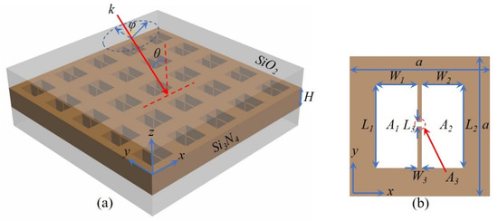
Figure 1.
(a) three-dimensional schematic diagram of dielectric metasurface with H-shaped nanoholes surrounded by SiO2; (b) x-y cross-section of the nanohole array in a lattice.
BICs are identified as localized states coexisting with extend modes within the light cone, and they have attracted tremendous attention due to their unbounded Q-factors. BICs concepts and physical mechanisms are presented in Refs. [14,30,42], and BICs are classified as follows:
The first one is the bound state due to symmetry or separability. It includes symmetry-protected BICs and separable BICs, which are associated with the coupling of certain resonances with the radiation modes are forbidden by symmetry or separability. When a system exhibits reflection or rotational symmetry, modes of different symmetry classes completely decouple.The second one is the bound state through parameter tuning. When the number of radiation channels is small, tuning the parameters of the system may be enough to completely suppress radiation into all channels.The third one is the bound state from inverse construction. If starting with a desired BIC, it is possible to design a system that can support this bound state and the continuous spectrum containing it. This inverse construction is achieved by engineering the potential, the hopping rate, or the boundary shape of the structure.
Figure 2 is the numerical reflectance spectra of the photonic crystal slab with an H-shaped nanohole array under a p-polarized plane wave. Two BICs at a normal incidence and one BIC at an oblique incidence are obtained in the picture. The former is the symmetry-protected BIC, which is associated with the coupling prohibition with the outgoing waves due to symmetry incompatibility, and the latter is the accidental BIC, which is attributed to the leakage canceled by interference [43]. The two symmetry-protected BICs happen at λ = 0.5647652 μm and 0.5343390 μm, respectively, with incident angle θ = 0°, and the accidental BIC occurs at λ = 0.6890324 μm with incident angle θ = 18.9°. These multiple BICs move as the structural parameters vary, in other words, they can be modulated flexibly by the parameters.
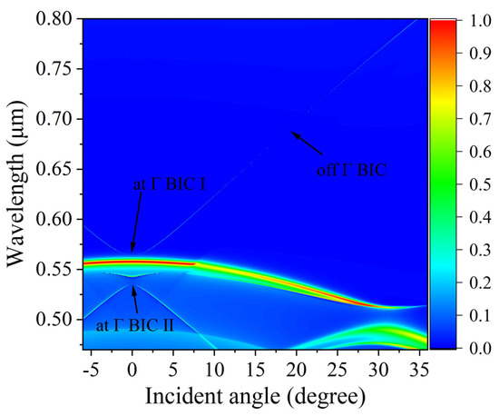
Figure 2.
Reflectance spectra of the metasurface under p-polarized plane wave. a = 0.336 μm, L1 = L2 = 0.2 μm, W1 = W2 = 0.1 μm.
To clarify the resonance behavior around at Γ BICs, we plot the spectra at 0.01°, 0.3°, and 0.5° in Figure 3a,c. It is shown clearly in Figure 3a that when the oblique incidence angle equals to 0.5°, a Fano resonance peak appears at λ = 0.565091 μm with full width at half maximum (FWHM) 5.95 × 10⁻⁶ μm. The width of the resonance peak narrows to zero when oblique incidence turns into normal incidence. In Figure 3c, the at Γ BICs occurs at about λ = 0.534064 μm at normal incidence, and it transforms into quasi-BICs with the incidence angle deviating from 0°.
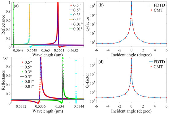
Figure 3.
The reflectance spectra of the metasurface extracted from Figure 2 simulated from FDTD (solid lines) and temporal CMT (circle dots) at the incidence angle (a) θ = 0.01°, 0.3°, 0.5°, around λ = 0.5647652 μm, (c) θ = 0.01°, 0.3°, 0.5°, around λ = 0.534339 μm, respectively. (b,d) are the different variations of the Q-factors of (a,c) reflectance resonance modes, including FDTD simulations of BIC (solid line) and CMT calculations (dots) at different incidence angles, respectively.
To investigate the physical properties of off Γ BIC and at Γ BIC in double-layer nanobars, we employed the coupled mode theory (CMT) [43,44,45,46,47] and compared the results with the FDTD simulation. The reflected amplitude r can be expressed as follows:
We can write the overall reflectance as:
We set , d1k1 = ƒγ, where τr is the radiative decay lifetime, τnr is the non-radiative decay lifetime, d1 represents the coefficients, and the factor ƒ is the complex amplitude of the resonant mode, which can be obtained as ƒ = tslab + rslab.
In order to further understand the physical properties of the BIC in the photonic crystal slab with H-shaped nanohole arrays, we plot the Q-factors of the high-quality resonances around BICs. Q-factors are calculated using the following equation:
where ω0 is the resonant frequency and γ is the damping rage of the structure.
Q = ω0/2γ
The Q-factors of the three BICs, as shown in Figure 3b,d. Q-factors in Figure 3b,d reaches 106. Q-factor is an important index to characterize a device’s performance. A device with ultrahigh Q-factor means it has excellent perception from the surrounding environment, which is significant in the sensing technology.
Figure 4a–c shows the reflectance spectra of the H-shaped nanohole structure under an oblique incidence around the off Γ BIC around 18.9°. The resonance peak locates at center wavelength of 0.6676519 μm for 16°, and its FWHM narrows to zero with the incidence angle increasing to 19° at about 0.6897667 μm. With the oblique incidence angle rising to 23°, FWHM is gradually widened and monotonously shifts to 0.7189055 μm. The zero width of the resonance peak means the BICs have an infinite lifetime without radiation. Figure 4d draws the Q-factor, and it theoretically exceeds 106.
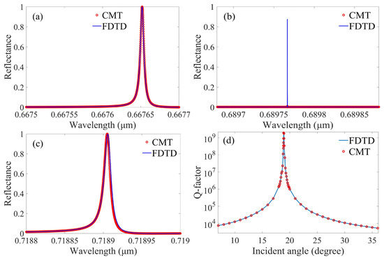
Figure 4.
The reflectance spectra of the metasurface extracted from Figure 2 simulated from FDTD (solid lines) and temporal CMT (circle dots) at the incidence angle (a) for the BIC at 16°, 0.6676519 μm, (b) for the BIC at 19° about 0.6897667 μm, and (c) for the BIC at 23°, about 0.7189055 μm. (d) Q-factor of the reflectance resonance modes including BIC from FDTD (solid lines) and CMT calculation (circle dots) as a function of incident angle of the H-shaped nanohole metasurface.
Above all, the Q-factors in Figure 3a,c tend to infinity at incident angle 0°, indicating two ideal BICs at the Γ points and that in Figure 4, they display a ultrahigh value at about 18.9°, revealing one ideal BIC at an off Γ point. The infinite Q-factor means that resonance has an infinite lifetime and the leakage resonance becomes a local eigenmode, which is perfectly limited. However, due to the surface roughness and material absorption, as well as the limited size of the sample, the Q-factor cannot reach the theoretical level. In Figure 3 and Figure 4, we simulate the reflectance spectra and Q-factors using the CMT method to confirm that from FDTD and the results from both methods accord well. Here, the various parameters are shown in Table 1.

Additionally, we plot the Ez component of the near-field distributions near-field distributions near the at BICs and off BIC of the metasurface, respectively. A tiny incident angle deviation is adopted to make sure that the radiation modes can be excited. Firstly, symmetrical distributions of Ez dipoles can be found in the x-y cross section and about the x-z plane in the z direction in Figure 5a–d, respectively. The dipoles are trapped inside the structure at the at Γ BIC mode as a result of the symmetry incompatibility between the trapped mode and the radiation incident wave. It is proved that the incident wave propagating inside the metasurface has various propagation constants in the z direction, which may reflect back into the slab or transmit into the surrounding medium. The interference and canceling from each transmitted wave from different channels lead to the off Γ BIC mode which is present at an appropriate k point, and light can be trapped in the structure, which can be confirmed in Figure 5e,f, respectively.
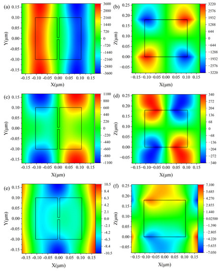
Figure 5.
Ez component of the near-field distributions of an incident angle near the BIC modes (a) at the x-y cross section at z = 0 μm and (b) at the x-z cross section, at y = 0 μm, θ = 0.01° and λ = 0.5647652 μm; (c) at the x-y cross section at z = 0 μm and (d) at the x-z cross section, at y = 0 μm, at θ = 0.01°, and λ = 0.534339 μm; (e) at x-y cross section at z = 0 μm and (f) at x-z cross section, at y = 0 μm, θ = 18.91°, and λ = 0.6891059 μm, of the H-shaped nanohole metasurface. a = 0.336 μm, L1 = L2 = 0.2 μm, W1 = W2 = 0.1 μm.
BICs are robust when system parameter changes occur, as shown in Figure 6. Consequently, we simulate the reflectance of the photonic crystal slab with the H-shaped nanohole array as the lattice constant changes to a = 0.316 μm, 0.336 μm, and 0.356 μm at Γ points and off Γ points, respectively. Figure 6a shows that two BICs located at Γ point at 0.50408 μm and 0.531757 μm in the reflectance spectra. As the lattice constant increases from 0.316 μm to 0.356 μm, the center wavelength of the two BICs redshifts obviously to 0.564374 μm and 0.596559 μm, with the distance between the two BICs widening from 0.060294 μm to 0.064802 μm as shown in Figure 6c. The results here are helpful in the design of optical devices based on multi-BICs. On the other hand, variation in the BIC at the off Γ point is simulated in Figure 6d–f as the lattice constant increases. The off Γ BIC happens at 18.7° and 0.64648 μm with a = 0.316 μm, and it occurs at 18.8° and 0.728704 μm with a = 0.356 μm, which means the lattice constant can modulate the incident angle and wavelength where the off Γ BIC appears.
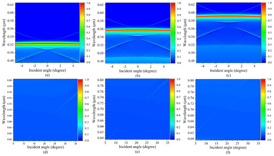
Figure 6.
Reflectance spectra of the metasurface around at Γ BICs with lattice constant (a) a = 0.316 μm, (b) a = 0.336 μm, and (c) a = 0.356 μm, respectively, and around off Γ BIC with lattice constant (d) a = 0.316 μm, (e) a = 0.336 μm, and (f) a = 0.356 μm, respectively. L1 = L2 = 0.2 μm, and W1 = W2 = 0.1 μm.
Figure 7 plots the reflectance spectra of the H-shaped nanohole array with L1 = L2 = 0.1 μm, 0.15 μm, and 0.2 μm. The two at Γ BICs blueshifts from 0.573068 μm and 0.547112 μm to 0.5647652 μm and 0.534339 μm, with L1 and L2 increasing from 0.1 μm to 0.2 μm, respectively, accompanied by a tiny variation in the distance between the two BICs by 0.00447 μm. In the meantime, the off Γ BIC moves to the location where the incident angle is 22.6° and the center wavelength is 0.729208 μm from 18.9° and 0.6890324 μm with L1 and L2 increasing from 0.1 μm to 0.2 μm, which indicates that the off Γ BIC can be modulated by the side length L1 and L2 of the H-shaped nanoholes.
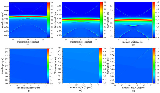
Figure 7.
Reflectance spectra of the metasurface around at Γ BICs with side length (a) L1 = L2 = 0.1 μm, (b) L1 = L2 = 0.15 μm, and (c) L1 = L2 = 0.2 μm, respectively, and around off Γ BIC with side length (d) L1 = L2 = 0.1 μm, (e) L1 = L2 = 0.15 μm, and (f) L1 = L2 = 0.2 μm, respectively. a = 0.336 μm, and W1 = W2 = 0.1 μm.
Similarly, the reflectance spectra of the H-shaped nanohole array around at Γ BICs and off Γ BIC are also simulated with side length W1 = W2 = 0.1 μm, W1 = W2 = 0.125 μm, and W1 = W2 = 0.15 μm, respectively, as shown in Figure 8. It is shown that the two at Γ BICs blueshifts from 0.5647652 μm and 0.534339 μm to 0.550831 μm and 0.51303 μm, with W1 and W2 evidently rising from 0.1 μm to 0.15 μm at normal incidence, accompanied by the off Γ BIC moving by 0.0311404 μm to the shorter wavelength monotonously.
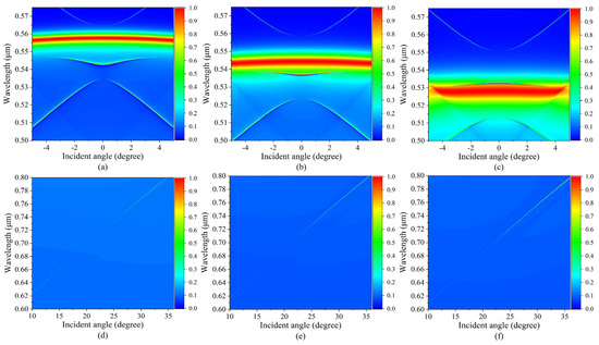
Figure 8.
Reflectance spectra of the metasurface around at Γ BICs with side length (a) W1 = W2 = 0.1 μm, (b) W1 = W2 = 0.125 μm, and (c) W1 = W2 = 0.15 μm, respectively, and around off Γ BIC with side length (d) W1 = W2 = 0.1 μm, (e) W1 = W2 = 0.125 μm, and (f) W1 = W2 = 0.15 μm, respectively. a = 0.336 μm, and L1 = L2 = 0.1 μm.
Furtherly, we move the center location of part A1 in y direction by 0.05 μm, and the center location of part A3 in −y direction by 0.05 μm, in the H-shaped nanoholes in order to study the influence of symmetry of the nanohole in the BICs, as shown in Figure 9. It is seen distinctly that the two BICs at Γ point disappear; however, the BIC at the oblique incident angle is affected insignificantly. We can modulate the presence of at Γ BICs only by adjusting the relative position of the parts in the nanoholes.
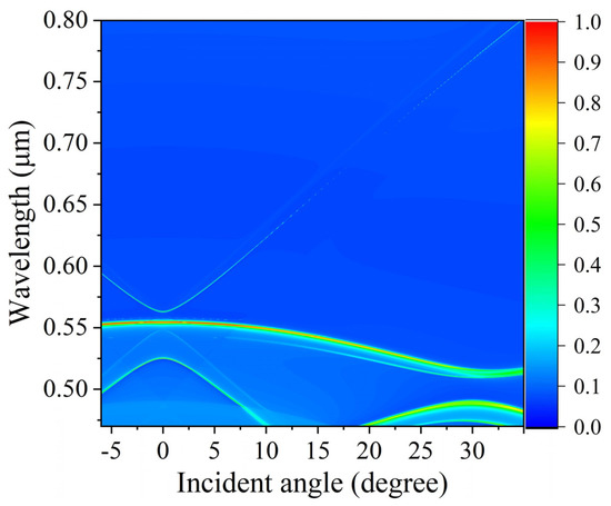
Figure 9.
Reflectance spectra of the metasurface with center position shifting by 0.05 μm in y direction of A1 and by 0.05 μm in −y direction of A2. a = 0.336 μm, L1 = L2 = 0.2 μm, W1 = W2 = 0.1 μm.
Figure 10 shows the center wavelength of the resonance modes as a function of the refractive index n2 of the surrounding medium for around (a) at Γ BIC I and (b) at Γ BIC II at incident angles 0.1°, 0.5°, and 1°, respectively, and (c) around off Γ BIC at incident angles 16°, 19°, and 23°, respectively. It is shown in Figure 10a that center wavelength of the resonance modes redshift obviously with n2 by a tiny increase. This is similarly shown in Figure 10b; however, at the same refractive index of the surrounding medium, the longer the center wavelength, the bigger the oblique incident angle is, which is opposite to what is shown in Figure 10a.
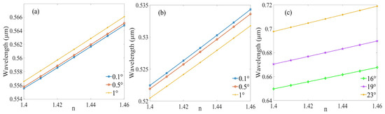
Figure 10.
The center wavelength of the resonance modes as functions of the refractive index n2 of the surrounding medium around (a) at Γ BIC I and (b) at Γ BIC II at incidence angles of 0.1°, 0.5°, and 1°, and (c) at off Γ BIC at incidence angles of 16°, 19°, and 23°, respectively. When n2 increases from 1.4 to 1.46 in steps of 0.01, the other structural parameters are n1 = 2.02, a = 0.336 μm, H = 0.18 μm, L1 = L2 = 0.2 μm, W1 = W2 = 0.1 μm.
We study the relationship between the resonant mode and the refractive index of the surrounding medium in the photonic crystal slab with the H-shaped nanohole array at incident angles θ = 16°, θ = 19°, and θ = 23°, respectively. The other structural parameters were n1 = 2.02, a = 0.336 μm, H = 0.18 μm, L1 = L2 = 0.2 μm, and W1 = W2 = 0.1 μm. Figure 10 shows the center wavelength of the resonance mode as a function of the refractive index of the surrounding medium. When the refractive index of the surrounding medium is n2 = 1.4, the center wavelength of the resonant mode at incident angles θ = 16° and θ = 23° is 0.649716 μm and 0.697755 μm, respectively. Then, the wavelength of the resonant peaks at incident angles of 16° and 23° redshifts with the increase in the surrounding refractive index. When the refractive index of the surrounding medium n2 = 1.46, the central wavelength increases by 0.6676519 μm and 0.7189055 μm at incident angles θ = 16° and θ = 23°, respectively. The results show that the resonance mode of the metasurface with the H-shaped nanohole are sensitive to the refractive index of the surrounding medium. Because the BICs have zero line width, it is hard to observe their movement directly. We extract two modes with a finite lifetime at 16° and 23° to obtain the changing rules of BICs because they behave similarly to the variation in the environment.
In order to investigate the influence of the H-shaped structure on the environmental refractive index, we use the figure of merit (FOM) to study the performance of this structure as a refractive index sensor. The calculation formula for FOM is shown below:
FOM = (∆λ⁄∆n(nm⁄RIU))/FWHM
As shown in Table 2, we calculated the FOM values for at Γ BIC I, at Γ BIC II, and the vicinity of off Γ BIC, with the refractive index of the surrounding medium n2 = 1.4. The results indicate that the FOM values can reach up to 105, making the H-shaped structure very sensitive to its surrounding environment. This is helpful for the research and development of sensors.
Table 2.
FOM for different BICs at different incidence angles.
Furthermore, we approach the reflectance spectra of the H-shaped nanohole array structure under the s-polarized plane wave. In Figure 11, we can see that there are two BICs located at Γ point, which we distinguish as BIC I and BIC II. These exhibit different phenomena when illuminated by p-polarized incident light. Additionally, we discovered the emergence of BIC III below BIC II, which is a very peculiar phenomenon. This could potentially lead to different research directions for the study of s-polarized light. On the other hand, when considering wavelength band, BIC under oblique incidence is also observed.
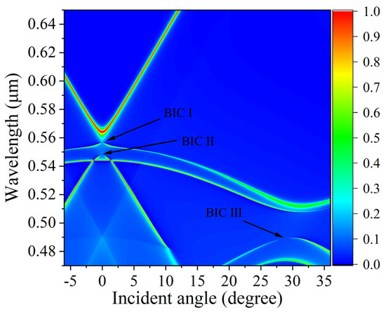
Figure 11.
Reflectance spectra of the metasurface under s-polarized plane wave. a = 0.336 μm, L1 = L2 = 0.2 μm, W1 = W2 = 0.1 μm.
3. Conclusions
Multiple optical BICs and their modulation of a metasurface consisting of a layer of Si3N4 H-shaped nanohole array, surrounded by a silica medium, are investigated. Ultrahigh Q-factors that exceed 106 are obtained from the all-dielectric nanostructure. Two at Γ BICs and one off Γ BIC appear in the reflectance spectra in the visible light band, and they can flexibly modulate by the lattice constant and the side length of the nanohole in one lattice. As the lattice constant increases, two at Γ BICs redshift, which is obviously accompanied by them departing to each other. Differently, the two at Γ BICs blueshift as the side length of part A1 and A2 rises. On the other hand, off Γ BICs shift with the structure parameters monotonously. Furthermore, if we break the symmetry of the H-shaped nanohole by moving center of A1 in the y direction and A2 in the −y direction, the two at Γ BICs both transform to quasi-BICs, but off Γ BICs are influenced insignificantly. Additionally, BICs of both types are ultra-sensitive to the surrounding medium. The results here are helpful in the design of photonic filters and sensors.
Author Contributions
S.X.: Funding acquisition, Investigation, Project administration, Resources, Software, Supervision, Validation, Visualization, Writing—original draft, Writing—review and editing. J.Y. and G.T.: Conceptualization, Data curation, Formal analysis, Investigation, Writing—original draft. W.S. and C.B., Methodology, Software, Investigation, Data curation. All authors have read and agreed to the published version of the manuscript.
Funding
This work was supported by Hunan Provincial Natural Science Foundation of China (Grant No. 2020JJ5153). National Natural Science Foundation of China (Grant No. 11304094, 12172228), the Program of Foundation of Science and Technology Commission of Shanghai Municipality (Grant No. 22dz1204202), and Natural Science Foundation of Shanghai (Grant No. 22ZR1444400). Horizontal Scientific Research Project (Grant No. H-2021-304-049, H-2021-304-128).
Institutional Review Board Statement
Not applicable.
Informed Consent Statement
Not applicable.
Data Availability Statement
All codes and data generated or analyzed during this study are included in this published article.
Acknowledgments
The data and methods used in the research are presented in sufficient detail in the document for other researchers to replicate the work.
Conflicts of Interest
The authors declare no conflict of interest.
References
- Ursell, F. Trapping modes in the theory of surface waves. Math. Proc. Camb. Philos. Soc. 1951, 47, 347–358. [Google Scholar] [CrossRef]
- Robnik, M. A simple separable Hamiltonian having bound states in the continuum. J. Phys. A Math. Gen. 1986, 19, 3845–3848. [Google Scholar] [CrossRef]
- Ursell, F. Trapped modes in a circular cylindrical acoustic waveguide. Proc. R. Soc. Lond. Ser. A Math. Phys. Sci. 1991, 435, 575–589. [Google Scholar]
- Evans, D.; Linton, C.; Ursell, F. Trapped mode frequencies embedded in the continuous spectrum. Q. J. Mech. Appl. Math. 1993, 46, 253–274. [Google Scholar] [CrossRef]
- Lee, J.; Zhen, B.; Chua, S.-L.; Qiu, W.; Joannopoulos, J.; Soljačić, M.; Shapira, O. Observation and differentiation of unique high-Q optical resonances near zero wave vector in macroscopic photonic crystal slabs. Phys. Rev. Lett. 2012, 109, 067401. [Google Scholar] [CrossRef]
- Hsu, C.W.; Zhen, B.; Lee, J.; Chua, S.-L.; Johnson, S.G.; Joannopoulos, J.D.; Soljačić, M. Observation of trapped light within the radiation continuum. Nature 2013, 499, 188–191. [Google Scholar] [CrossRef]
- Bulgakov, E.N.; Sadreev, A.F. Bound states in the continuum in photonic waveguides inspired by defects. Phys. Rev. B 2008, 78, 075105. [Google Scholar] [CrossRef]
- Plotnik, Y.; Peleg, O.; Dreisow, F.; Heinrich, M.; Nolte, S.; Szameit, A.; Segev, M. Experimental Observation of Optical Bound States in the Continuum. Phys. Rev. Lett. 2011, 107, 183901. [Google Scholar] [CrossRef]
- Weimann, S.; Xu, Y.; Keil, R.; Miroshnichenko, A.; Tünnermann, A.; Nolte, S.; Sukhorukov, A.; Szameit, A.; Kivshar, Y.S. Compact Surface Fano States Embedded in the Continuum of Waveguide Arrays. Phys. Rev. Lett. 2013, 111, 240403. [Google Scholar] [CrossRef]
- González, J.W.; Pacheco, M.; Rosales, L.; Orellana, P.A. Bound states in the continuum in graphene quantum dot structures. EPL Europhys. Lett. 2010, 91, 66001. [Google Scholar] [CrossRef]
- Azzam, S.I.; Shalaev, V.M.; Boltasseva, A.; Kildishev, A.V. Formation of Bound States in the Continuum in Hybrid Plasmonic-Photonic Systems. Phys. Rev. Lett. 2018, 121, 253901. [Google Scholar] [CrossRef] [PubMed]
- Sadrieva, Z.; Frizyuk, K.; Petrov, M.; Kivshar, Y.; Bogdanov, A. Multipolar origin of bound states in the continuum. Phys. Rev. B 2019, 100, 115303. [Google Scholar] [CrossRef]
- Kupriianov, A.S.; Xu, Y.; Sayanskiy, A.; Dmitriev, V.; Kivshar, Y.S.; Tuz, V.R. Metasurface Engineering through Bound States in the Continuum. Phys. Rev. Appl. 2019, 12, 014024. [Google Scholar] [CrossRef]
- Hsu, C.W.; Zhen, B.; Stone, D.; Joannopoulos, J.; Soljačić, M. Bound states in the continuum. Nat. Rev. Mater. 2016, 1, 1–13. [Google Scholar] [CrossRef]
- Xu, L.; Rahmani, M.; Ma, Y.; Smirnova, D.A.; Kamali, K.Z.; Deng, F.; Chiang, Y.K.; Huang, L.; Zhang, H.; Gould, S.; et al. Enhanced light–matter interactions in dielectric nanostructures via machine-learning approach. Adv. Photon. 2020, 2, 026003. [Google Scholar] [CrossRef]
- Huang, L.; Xu, L.; Rahmani, M.; Neshev, D.; Miroshnichenko, A.E. Pushing the limit of high-Q mode of a single dielectric nanocavity. Adv. Photon. 2021, 3, 016004. [Google Scholar] [CrossRef]
- Huang, L.; Xu, L.; Woolley, M.; Miroshnichenko, A. Trends in quantum nanophotonics. Adv. Quantum Technol. 2020, 3, 1900126. [Google Scholar] [CrossRef]
- Liu, T.; Qin, M.; Wu, F.; Xiao, S. High-efficiency optical frequency mixing in an all-dielectric metasurface enabled by multiple bound states in the continuum. Phys. Rev. B 2023, 107, 075441. [Google Scholar] [CrossRef]
- Xiao, S.; Qin, M.; Duan, J.; Wu, F.; Liu, T. Polarization-controlled dynamically switchable high-harmonic generation from all-dielectric metasurfaces governed by dual bound states in the continuum. Phys. Rev. B 2022, 105, 195440. [Google Scholar] [CrossRef]
- von Neumann, J.; Wigner, E. Über merkwürdige diskrete Eigenwerte. In The Collected Works of Eugene Paul Wigner: Part A: The Scientific Papers; Springer: Berlin/Heidelberg, Germany, 1993; pp. 291–293. [Google Scholar]
- Watts, M.R.; Johnson, S.; Haus, H.A.; Joannopoulos, J.D. Electromagnetic cavity with arbitrary Q and small modal volume without a complete photonic bandgap. Opt. Lett. 2002, 27, 1785–1787. [Google Scholar] [CrossRef]
- Marinica, D.C.; Borisov, A.G.; Shabanov, S.V. Bound States in the Continuum in Photonics. Phys. Rev. Lett. 2008, 100, 183902. [Google Scholar] [CrossRef]
- Molina, M.I.; Miroshnichenko, A.E.; Kivshar, Y.S. Surface Bound States in the Continuum. Phys. Rev. Lett. 2012, 108, 070401. [Google Scholar] [CrossRef]
- Hsu, C.W.; Zhen, B.; Chua, S.-L.; Johnson, S.G.; Joannopoulos, J.D.; Soljačić, M. Bloch surface eigenstates within the radiation continuum. Light. Sci. Appl. 2013, 2, e84. [Google Scholar] [CrossRef]
- Linton, C.; McIver, P. Embedded trapped modes in water waves and acoustics. Wave Motion 2007, 45, 16–29. [Google Scholar] [CrossRef]
- Hirose, K.; Liang, Y.; Kurosaka, Y.; Watanabe, A.; Sugiyama, T.; Noda, S. Watt-class high-power, high-beam-quality photonic-crystal lasers. Nat. Photon. 2014, 8, 406–411. [Google Scholar] [CrossRef]
- Wierer, J.J.; David, A.; Megens, M.M. III-nitride photonic-crystal light-emitting diodes with high extraction efficiency. Nat. Photon 2009, 3, 163–169. [Google Scholar] [CrossRef]
- Ganesh, N.; Zhang, W.; Mathias, P.; Chow, E.; Soares, J.A.N.T.; Malyarchuk, V.; Smith, A.D.; Cunningham, B.T. Enhanced fluorescence emission from quantum dots on a photonic crystal surface. Nat. Nanotechnol. 2007, 2, 515–520. [Google Scholar] [CrossRef]
- Zhen, B.; Chua, S.-L.; Lee, J.; Rodriguez, A.W.; Liang, X.; Johnson, S.G.; Joannopoulos, J.D.; Soljačić, M.; Shapira, O. Enabling enhanced emission and low-threshold lasing of organic molecules using special Fano resonances of macroscopic photonic crystals. Proc. Natl. Acad. Sci. USA 2013, 110, 13711–13716. [Google Scholar] [CrossRef] [PubMed]
- Zhen, B.; Hsu, C.W.; Lu, L.; Stone, A.D.; Soljačić, M. Topological Nature of Optical Bound States in the Continuum. Phys. Rev. Lett. 2014, 113, 257401. [Google Scholar] [CrossRef] [PubMed]
- Fan, S.; Joannopoulos, J.D. Analysis of guided resonances in photonic crystal slabs. Phys. Rev. B 2002, 65, 235112. [Google Scholar] [CrossRef]
- Pacradouni, V.; Mandeville, W.; Cowan, A.; Paddon, P.; Young, J.; Johnson, S. Photonic band structure of dielectric membranes periodically textured in two dimensions. Phys. Rev. B 2000, 62, 4204. [Google Scholar] [CrossRef]
- Yoon, J.W.; Song, S.H.; Magnusson, R. Critical field enhancement of asymptotic optical bound states in the continuum. Sci. Rep. 2015, 5, 18301. [Google Scholar] [CrossRef] [PubMed]
- Fan, S.; Suh, W.; Joannopoulos, J.D. Temporal coupled-mode theory for the Fano resonance in optical resonators. J. Opt. Soc. Am. A 2003, 20, 569–572. [Google Scholar] [CrossRef]
- Wu, F.; Luo, M.; Wu, J.; Fan, C.; Qi, X.; Jian, Y.; Liu, D.; Xiao, S.; Chen, G.; Jiang, H.; et al. Dual quasibound states in the continuum in compound grating waveguide structures for large positive and negative Goos-Hänchen shifts with perfect reflection. Phys. Rev. A 2021, 104, 023518. [Google Scholar] [CrossRef]
- Wang, X.; Duan, J.; Chen, W.; Zhou, C.; Liu, T.; Xiao, S. Controlling light absorption of graphene at critical coupling through magnetic dipole quasi-bound states in the continuum resonance. Phys. Rev. B 2020, 102, 155432. [Google Scholar] [CrossRef]
- Hu, Y.; Tong, M.; Hu, S.; He, W.; Cheng, X.; Jiang, T. Spatiotemporal Lineshape Tailoring in BIC-Mediated Reconfigurable Metamaterials. Adv. Funct. Mater. 2022, 32, 2203680. [Google Scholar] [CrossRef]
- Hu, Y.; Xie, S.; Bai, C.; Shen, W.; Yang, J. Multiple photonic bound states in the continuum in an electromagnetically induced transparency metasurface. IEEE Photon. J. 2022, 14, 1–9. [Google Scholar] [CrossRef]
- Liu, Z.; Xu, Y.; Lin, Y.; Xiang, J.; Feng, T.; Cao, Q.; Li, J.; Lan, S.; Liu, J. High-Q quasibound states in the continuum for nonlinear metasurfaces. Phys. Rev. Lett. 2019, 123, 253901. [Google Scholar] [CrossRef]
- Xie, S.; Xie, S.; Zhan, J.; Xie, C.; Tian, G.; Li, Z.; Liu, Q. Bound States in the Continuum in a T-Shape Nanohole Array Perforated in a Photonic Crystal Slab. Plasmonics 2020, 15, 1261–1271. [Google Scholar] [CrossRef]
- Xie, S.; Xie, S.; Li, Z.; Tian, G.; Zhan, J.; Liu, Q. Observation of an Optical Bound State in Photonic Crystal Slabs with U-Shape Nanohole Array. Plasmonics 2021, 17, 399–407. [Google Scholar] [CrossRef]
- Li, H.; Zhou, H.; Wei, G.; Xu, H.; Qin, M.; Liu, J.; Wu, F. Photonic spin-selective perfect absorptance on planar metasurfaces driven by chiral quasi-bound states in the continuum. Nanoscale 2023, 15, 6636–6644. [Google Scholar] [CrossRef] [PubMed]
- Huang, L.; Xu, L.; Powell, D.A.; Padilla, W.J.; Miroshnichenko, A.E. Resonant leaky modes in all-dielectric metasystems: Fundamentals and applications. Phys. Rep. 2023, 1008, 1–66. [Google Scholar] [CrossRef]
- Liu, C.; Li, H.; Xu, H.; Zhao, M.; Xiong, C.; Zhang, B.; Wu, K. Slow light effect based on tunable plasmon-induced transparency of monolayer black phosphorus. J. Phys. D Appl. Phys. 2019, 52, 405203. [Google Scholar] [CrossRef]
- Zhang, B.; Li, H.; Xu, H.; Zhao, M.; Xiong, C.; Liu, C.; Wu, K. Absorption and slow-light analysis based on tunable plasmon-induced transparency in patterned graphene metamaterial. Opt. Express 2019, 27, 3598–3608. [Google Scholar] [CrossRef] [PubMed]
- Suh, W.; Wang, Z.; Fan, S. Temporal coupled-mode theory and the presence of non-orthogonal modes in lossless multimode cavities. IEEE J. Quantum Electron. 2004, 40, 1511–1518. [Google Scholar] [CrossRef]
- Li, H.; Wei, G.; Zhou, H.; Xiao, H.; Qin, M.; Xia, S.; Wu, F. Polarization-independent near-infrared superabsorption in transition metal dichalcogenide Huygens metasurfaces by degenerate critical coupling. Phys. Rev. B 2022, 105, 165305. [Google Scholar] [CrossRef]
Disclaimer/Publisher’s Note: The statements, opinions and data contained in all publications are solely those of the individual author(s) and contributor(s) and not of MDPI and/or the editor(s). MDPI and/or the editor(s) disclaim responsibility for any injury to people or property resulting from any ideas, methods, instructions or products referred to in the content. |
© 2023 by the authors. Licensee MDPI, Basel, Switzerland. This article is an open access article distributed under the terms and conditions of the Creative Commons Attribution (CC BY) license (https://creativecommons.org/licenses/by/4.0/).