Communication

All-Monolithically Integrated Self-Scanning Addressable VCSEL Array for 3D Sensing

FUJIFILM Business Innovation Corp., Ebina-shi 243-0494, Japan
*
Author to whom correspondence should be addressed.
Photonics 2023, 10(3), 304; https://doi.org/10.3390/photonics10030304
Submission received: 29 January 2023 / Revised: 6 March 2023 / Accepted: 8 March 2023 / Published: 13 March 2023

Abstract

:
We propose an all-monolithically integrated self-scanning addressable vertical-cavity surface-emitting laser array for time-of-flight measurement. Some advantages of addressable VCSELs for ToF measurement applications include large reductions in power consumption, heat generation, multi-pass noise, and flare noise. In this paper, we discuss the characteristics of the proposed self-scanning addressable VCSEL array. All layers in the epilayer structure of the proposed VCSEL array were formed at once by metal-organic chemical vapor deposition. The device consists of an (Al)GaAs-based thyristor and a conventional top-emitting 940-nm oxide-confined VCSEL on an n-type GaAs substrate. The array contained 12 blocks (4 × 3) that have more than 40 emitters each. The device required only four signals from a field-programmable gate array to select the emitting blocks and one emission signal from a conventional VCSEL driver, even for arrays containing hundreds of blocks. The proposed module is capable of one-block sequential emission, parallel emission from several blocks, and emission from all blocks. The rise and fall times of the fabricated VCSEL array were observed to be 200 and 400 ps, respectively, for each emission mode. The influence of flare noise from an obstacle in front of the camera was dramatically reduced by avoiding emission to the obstacle.

1. Introduction

Vertical-cavity surface-emitting lasers (VCSELs) are commonly used as light sources for optical communication, printers, heating, illumination, and sensor applications for cell phones, robots, and vehicles [1,2,3,4,5,6,7]. In particular, VCSELs are highly promising as a light source for 3D sensing owing to their high-power conversion efficiency, small wavelength drift against temperature, and low cost. Furthermore, the market for VCSELs in 3D sensing applications is growing dramatically.
A well-known technique for 3D sensing is time-of-flight (ToF) measurement, which is commonly used in the measurement range of 1 m to several hundred meters [6,7,8,9,10,11]. VCSEL technology is mainly applied to ToF measurements from below 1 m to several meters. However, this technique has limitations, as shown in Figure 1: (1) measurement error due to flare noise or multi-pass noise from floors, walls, and ceilings [12,13,14]; (2) poor distance measurement performance for low-reflective objects or those at long distances or in high-noise environments under the sun [15]; and (3) large power consumption and heat generation. These issues have prevented the widespread adoption of ToF systems. Addressable VCSEL is a key technology to overcome these limitations by avoiding emission obstacles. All the power is injected into one area of the VCSEL array, thereby increasing optical power density. Specific emission areas are selected to optimize power consumption and heat generation.
In this study, we developed an all-monolithically integrated self-scanning addressable VCSEL (SS-VCSEL) that has small circuits based on self-scanning light emitting device (SLED) technology composed of thyristors [16,17]. The thyristor has many advantages. For example, applying a small gate current can change the thyristor to the on-state, which can be maintained regardless of the gate voltage after switching. The thyristor is also highly tolerant against high currents and voltages, and exhibits high-speed switching below 10 ns [18]. An emitting diode, such as a VCSEL, of a device that has a diode-on-thyristor (DoT) structure is electrically connected to a switching thyristor in series through a tunnel junction.

2. Materials and Methods

Figure 2 shows a cross-sectional view of a conventional top-emitting 940-nm oxide-confined VCSEL with a single junction-emission region on a thyristor fabricated by us. There are 22 pairs p-Al0.15GaAs/Al0.9GaAs DBRs, 45 pairs n-Al0.15GaAs/Al0.95GaAs DBRs, and 3 InGaAs/AlGaAs quantum wells as an active layer. The thyristor is made of pnpn (Al)GaAs layers on an n-GaAs substrate. The VCSEL is connected in series to the thyristor through a GaAs-based tunnel junction. All layers in the epilayer structure are formed at once by metal-organic chemical vapor deposition. The VCSEL emits light if the voltage of the n-gate is changed to the on-level, and the n and p electrodes are supplied with a forward voltage that is larger than the threshold voltages of the VCSEL and the thyristor. Figure 3 shows an equivalent circuit of the proposed SS-VCSEL. The transmission region comprises transmission thyristors, diodes, and resistances. The on-state of the transmission thyristor is shifted to the next transmission thyristor sequentially by applying transmission signals 1 and 2 in order. The VCSEL that is connected to a transmission thyristor in the on-state emits light by adding an emission signal.
Figure 4 shows the top view of the proposed SS-VCSEL for ToF measurement. The array is composed of a transmission region (right side of the chip), an emission region (left side of the chip), five bonding pads on the top, and one electrode on the bottom of the substrate. The emission region comprises a 4 × 3 array of blocks. Each block includes 41 emitters. The device size is 1.2 mm × 1.1 mm. The anode and cathode metals are the same as those of a conventional VCSEL array. The bonding pads are for the two transmission signals, a constant voltage, and emission signals.
Figure 5 shows a top view of the transmission module containing the proposed SS-VCSEL. The field-programmable gate array (FPGA) on the left side of the module provides a minimum pulse width of 2.5 ns to control transmission and emission signals. The high voltage of the FPGA is 3.3 V. The SS-VCSEL, optical device, and commercial low-side laser diode driver (LDD) are situated on the right side of the module. The LDD can apply a maximum current of 3.6 A to the VCSEL by inputting the emission signal from the FPGA. The anode voltage of the SS-VCSEL can be changed up to 12 V, as shown in Figure 6.

3. Results

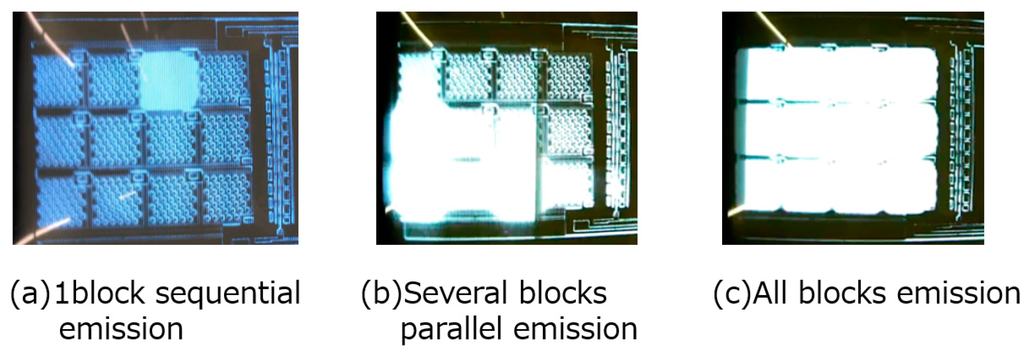
Figure 7 shows the emission pattern of the SS-VCSEL generated by applying the transmission and emission signals. One-block sequential emission, parallel emission from several blocks, and emission from all blocks are possible by changing the input signals.
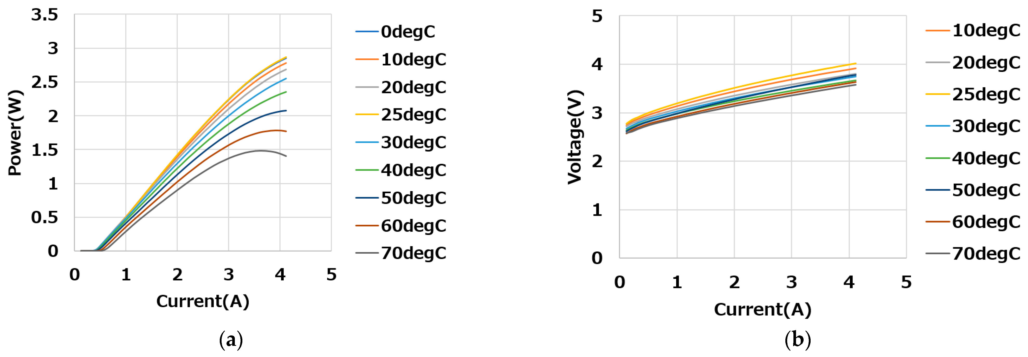
The current–light and current–voltage characteristics of the VCSEL on the thyristor in the all-blocks emission mode are shown in Figure 8. The device was operated using a pulse width and duty cycle of 1 ms and 1%, respectively. The IL characteristics of the SS-VCSEL are identical to those of conventional VCSELs. Additionally, the threshold voltage of the SS-VCSEL is higher than that of conventional VCSELs because the thyristor is connected to the VCSEL in series.
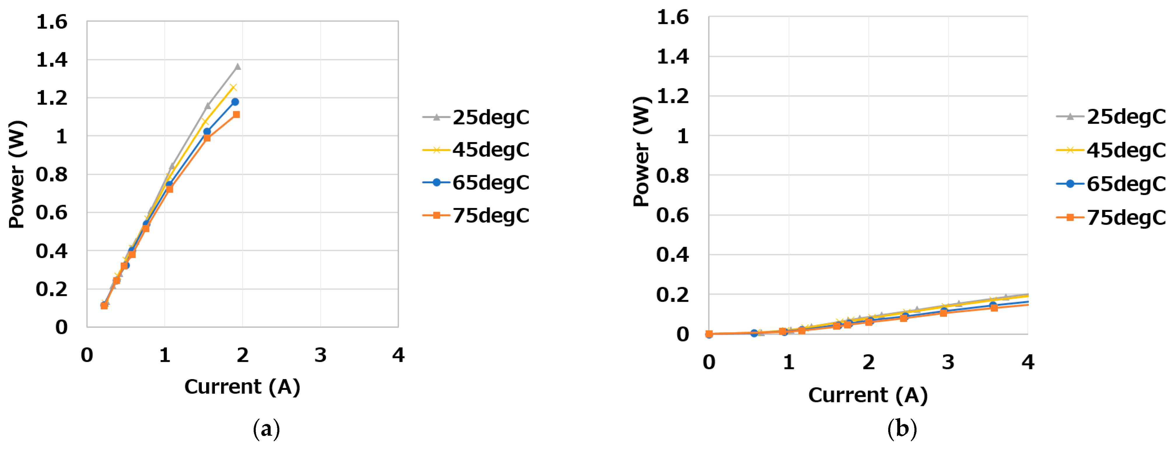
Figure 9a,b show the IL characteristics of the fabricated SS-VCSEL on the Tx module at different temperatures corresponding to one-block and all-blocks emissions, respectively. In Figure 9b, the vertical axis is the output power per block of the all-blocks emission mode. The module was operated using a pulse width and duty cycle of 10 ns and 5%, respectively. An optical output power of over 1 W was achieved during one-block emission at 75 °C. This result was 19 times higher than that of a single block in the all-blocks emission mode at a current of 2 A. The overall output power was 1.1 W/block × 12 blocks or 13 W at a temperature of 75 °C.
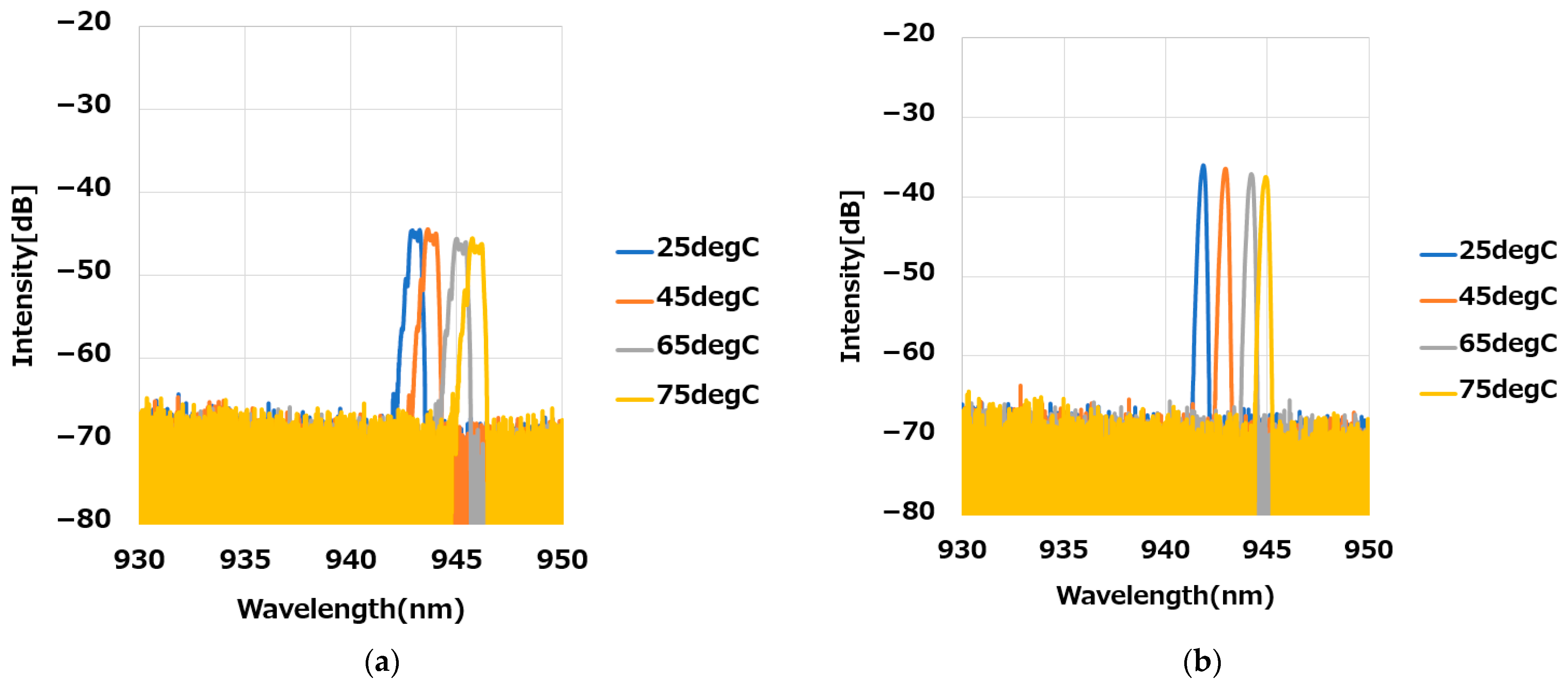
The SS-VCSEL output spectra of the Tx module at different temperatures obtained in the one-block and all-blocks emission modes are shown in Figure 10a,b, respectively. The current in the one-block and all-blocks emission modes were 2 A (49 mA/emitter) and 3.5 A (7 mA/emitter), respectively. The module was operated using a pulse width and duty cycle of 10 ns and 5%, respectively. The peak wavelengths during one-block emission and all-blocks emission at 25 °C were 943.0 and 941.8 nm, respectively. Narrow spectrum widths of 0.6 and 0.27 nm were achieved in the one-block and all-blocks emission modes, respectively. The spectrum width of one-block emission modes is wider than that of all-blocks emission modes due to the number of transverse modes with higher injected current density. The wavelength shift owing to changes in temperature was 0.06 nm.
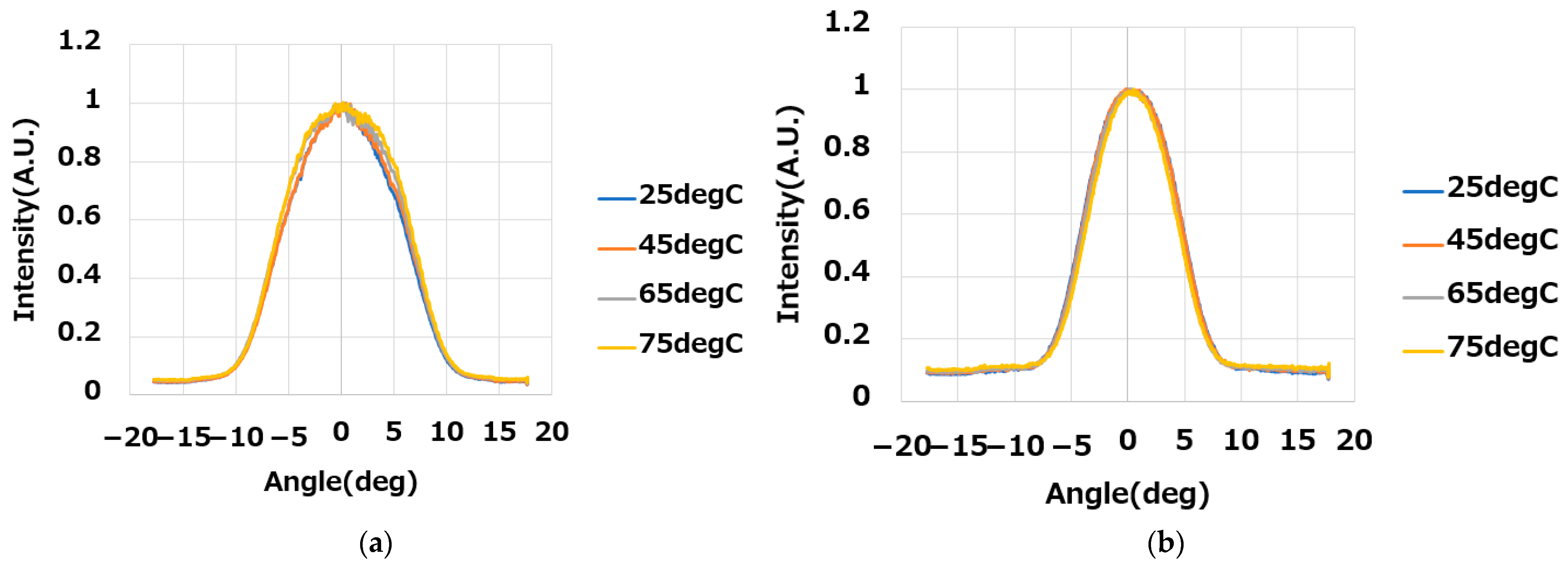
Figure 11a,b shows the far-field patterns of the SS-VCSEL on the Tx module at different temperatures in the one-block and all-blocks emission modes, respectively. The current during one-block and all-blocks emission were 2 A (49 mA/emitter) and 3.5 A (7 mA/emitter), respectively. The module was operated using a pulse width and duty cycle of 10 ns and 5%, respectively. The divergence angles corresponding to one-block and all-blocks emissions at 25 °C were 18.9° and 13.5°, respectively. The divergence angles of one-block emission modes is wider than that of all-blocks emission modes due to the number of transverse modes with higher injected current density. The profiles and divergence angles were stable in the temperature range of 25–75 °C.
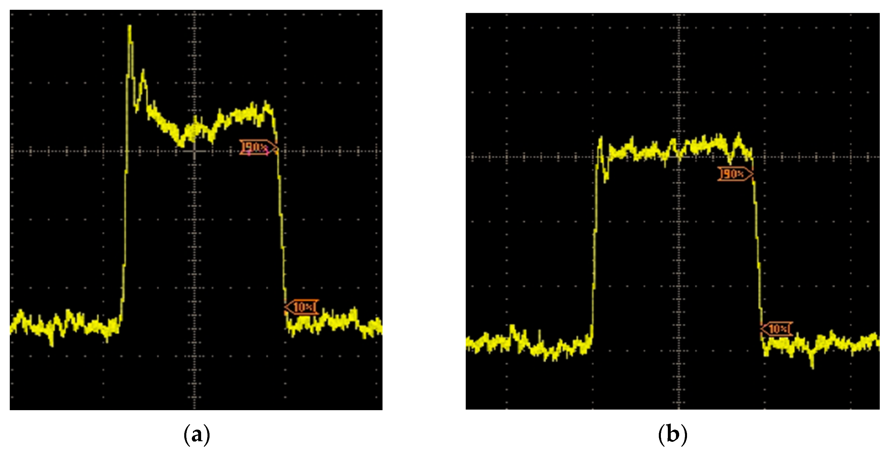
Figure 12a,b show the pulse operation in the one-block and all-blocks emissions modes, respectively. The module was operated using a pulse width and duty cycle of 10 ns and 5%, respectively. The rise times during all-blocks and one-block emissions were 243 and 282 ps, respectively. Therefore, a good rise time was achieved for application in the direct ToF system. The overshot in Figure 12a is a conventional relaxation oscillation of the lasing. The fall times during one-block and all-blocks emissions were less than 500 ps. The shape of the optical pulse from a single block can be optimized by changing the parameters of the VCSEL driver for indirect ToF systems. The pulse width can be shortened up to 2.5 ns by keeping rise time and fall time the same for one-block and all-blocks emissions.

4. Discussion

Figure 13 shows a comparison between the current–optical power density characteristics of a conventional three-junction VCSEL array with approximately 500 emitters and one-block and all-blocks emission of an SS-VCSEL with a single-junction active layer. Even though the optical power density of the all-blocks SS-VCSEL emission is lower than that of the conventional multi-junction VCSEL because of the number of junctions of active layers, the power density of one-block emission is higher than that of the multi-junction VCSEL. This result shows that the signal-to-noise (S/N) ratio is higher, the measurement distance is longer, and the power consumption and heat generation are lower when using the SS-VCSEL in comparison with those of the conventional multi-junction VCSEL. Moreover, the SS-VCSEL optical power density can be increased further by applying a multi-junction active layer.
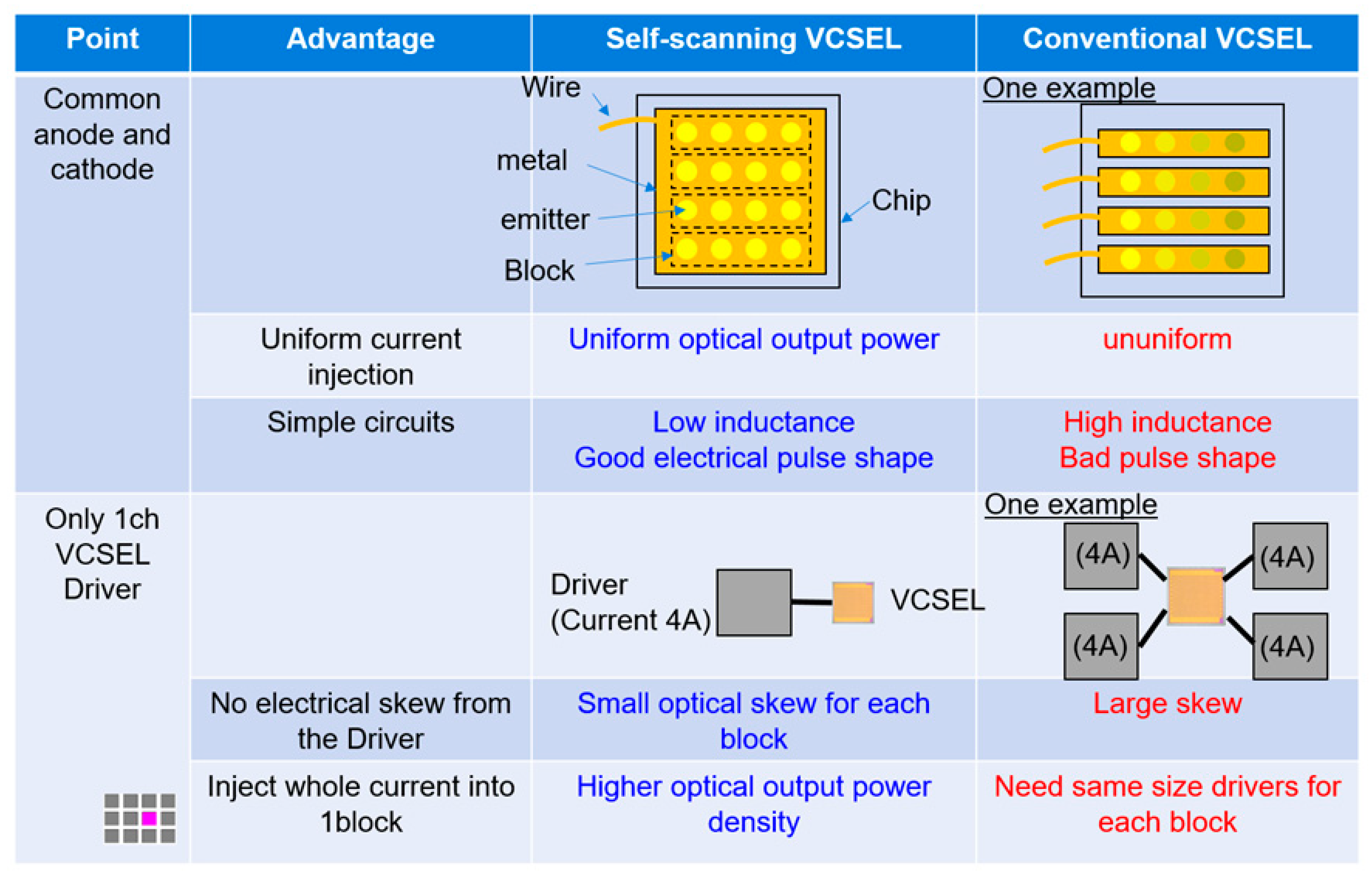
The advantages of the proposed SS-VCSEL over conventional addressable VCSELs are the following in Figure 14. The SS-VCSEL has a common anode and cathode metal that enables the uniform injection of current into each emitter in the block and the realization of simple circuits to minimize inductance. Moreover, the SS-VCSEL requires only a one-channel driver, even if the number of blocks exceed 100. No electrical skew occurs from the driver, and all currents can be injected into a single block.

5. Conclusions

We successfully designed, fabricated, and evaluated an all-monolithically integrated SS-VCSEL array that contains 12 blocks with 41 top-emitting VCSELs in each block for application to ToF systems. Any block emission mode can be realized. The optical power density of the proposed SS-VCSEL can exceed that of a conventional three-junction VCSEL owing to the concentration of the current on one block without lethal heating, despite the SS-VCSEL having a single-junction active layer. Further increases in optical power density can be realized by applying a multi-junction active layer. The rise time of the proposed SS-VCSEL was below 500 ps, and a good optical pulse shape was achieved. The number of blocks can be increased up to 100 without increasing the number of pads on the chip, resulting in much smaller chip and module sizes compared with other addressable VCSEL arrays. The SS-VCSEL is a highly promising light source for ToF systems.

Author Contributions

Conceptualization, T.K. and S.O.; methodology, T.K, J.H., T.S., D.I. and M.M.; validation, T.K., T.H. and K.T.; supervision, H.U. All authors have read and agreed to the published version of the manuscript.

Funding

This research received no external funding.

Institutional Review Board Statement

Not applicable.

Informed Consent Statement

Not applicable.

Data Availability Statement

Data sharing not applicable.

Conflicts of Interest

The authors declare no conflict of interest.

References

  1. Dalir, H.; Koyama, F. Bandwidth enhancement of single-mode VCSEL with lateral optical feedback of slow light. IEICE Electron. Exp. 2011, 8, 1075–1081. [Google Scholar] [CrossRef] [Green Version]
  2. Kondo, T.; Takeda, K.; Otoma, H.; Murakami, A.; Sakurai, J.; Nakayama, H.; Gu, X.; Koyama, F. Developments of VCSELs for printers and optical communications at Fuji Xerox. In Vertical-Cavity Surface-Emitting Lasers XX; SPIE: Bellingham, WA, USA, 2016; Volume 9766, pp. 51–59. [Google Scholar]
  3. Seurin, J.F.; Ghosh, C.L.; Khalfin, V.; Miglo, A.; Xu, G.; Wynn, J.D.; Pradhan, P.; D’Asaro, L.A. High-power high efficiency 2D VCSEL arrays. In Vertical-Cavity Surface-Emitting Lasers XII; SPIE: Bellingham, WA, USA, 2008; Volume 6908, pp. 45–58. [Google Scholar]
  4. Seurin, J.F.; Zhou, D.; Xu, G.; Miglo, A.; Li, D.; Chen, T.; Guo, B.; Ghosh, C. High-efficiency VCSEL arrays for illumination and sensing in consumer applications. In Vertical-Cavity Surface-Emitting Lasers XX; SPIE: Bellingham, WA, USA, 2016; Volume 9766, pp. 60–68. [Google Scholar]
  5. Grabherr, M. New applications boost VCSEL quantities: Recent developments at Philips. In Vertical-Cavity Surface-Emitting Lasers XIX; SPIE: Bellingham, WA, USA, 2015; Volume 9381, p. 938102. [Google Scholar]
  6. Moench, H.; Carpaij, M.; Gerlach, P.; Groneborn, S.; Gudde, R.; Hellmig, J.; Kolb, J.; van der Lee, A. VCSEL-based sensors for distance and velocity. In Vertical-Cavity Surface-Emitting Lasers XX; SPIE: Bellingham, WA, USA, 2016; Volume 9766, pp. 40–50. [Google Scholar]
  7. Warren, M.E.; Podva, D.; Dacha, P.; Block, M.K.; Helms, C.J.; Maynard, J. Low-divergence high-power VCSEL arrays for lidar application. In Vertical-Cavity Surface-Emitting Lasers XXII; SPIE: Bellingham, WA, USA, 2018; Volume 10552, pp. 72–81. [Google Scholar]
  8. Bamji, C.S.; Mehta, S.; Thompson, B.; Elkhatib, T.; Wurster, S.; Akkaya, O.; Payne, A.; Godbaz, J.; Fenton, M.; Rajasekaran, V.; et al. 1Mpixel 65 nm BSI 320 MHz demodulated TOF image sensor with 3.5 μm global shutter pixels and analog binning. In Proceedings of the 2018 IEEE International Solid-State Circuits Conference—(ISSCC), San Francisco, CA, USA, 11–15 February 2018; pp. 94–96. [Google Scholar]
  9. Kato, Y.; Sano, T.; Moriyama, Y.; Maeda, S.; Yamazaki, T.; Nose, A.; Shiina, K.; Yasu, Y.; Van der Tempel, W.; Ercana, A.; et al. 320 × 240 back-illuminated 10-μm CAPD pixels for high-speed modulation time-of-flight CMOS image sensor. IEEE J. Solid-State. Circuits 2018, 53, 1071–1078. [Google Scholar] [CrossRef]
  10. Shirakawa, Y.; Yasutomi, K.; Kagawa, K.; Aoyama, S.; Kawahito, S. An 8-Tap CMOS lock-in pixel image sensor for short-pulse time-of-flight measurements. Sensors 2020, 20, 1040. [Google Scholar] [CrossRef] [PubMed] [Green Version]
  11. Tontini, A.; Gasparini, L.; Perenzoni, M. Numerical model of SPAD-based direct time-of-flight flash lidar CMOS image sensors. Sensors 2020, 20, 5203. [Google Scholar] [CrossRef] [PubMed]
  12. Foix, S.; Alenya, G.; Torras, C. Lock-in time-of-flight (ToF) cameras: A survey. IEEE Sens. J. 2011, 11, 1917–1926. [Google Scholar] [CrossRef] [Green Version]
  13. Naik, N.; Kadambi, A.; Rhemann, C.; Izadi, S.; Raskar, R.; Kang, S.B. A light transport model for mitigating multipath interference in time-of-flight sensors. In Proceedings of the 2015 IEEE Conference on Computer Vision and Pattern Recognition (CVPR), Boston, MA, USA, 7–12 June 2015; pp. 73–81. [Google Scholar]
  14. Mure-Dubois, J.; Hügli, H. Real-time scattering compensation for time-of-flight camera. In Proceedings of the Proceedings of the ICVS Workshop on Camera Calibration Methods for Computer Vision Systems, Bielefeld, Germany, 21–24 March 2007. [Google Scholar]
  15. Lange, R.; Seitz, P. Solid-state time-of-flight range camera. IEEE J. Quantum Electron. 2001, 37, 390–397. [Google Scholar] [CrossRef] [Green Version]
  16. Kondo, T. All monolithically integrated self-scanning vertical-cavity surface-emitting array. In Proceedings of the 2018 IEEE International Semiconductor Laser Conference (ISLC), Santa Fe, NM, USA, 16–19 September 2018; pp. 1–2. [Google Scholar]
  17. Kondo, T.; Kitsunai, M.; Komagata, S.; Ohno, S.; Usami, H. Temperature characteristics of all-monolithically integrated self-scanning VCSEL array. In Vertical-Cavity Surface-Emitting Lasers XXIII; SPIE: Bellingham, WA, USA, 2019; Volume 10938, pp. 34–43. [Google Scholar]
  18. Kuijk, M.; Heremans, P.L.; Borghs, G.; Vounckx, R. Depleted double-heterojunction optical thyristor. Appl. Phys. Lett. 1994, 64, 2073–2075. [Google Scholar] [CrossRef]
Figure 1. Problems associated with ToF systems.
Photonics 10 00304 g001
Figure 2. Cross-sectional view of a conventional top-emitting 940-nm oxide-confined VCSEL.
Photonics 10 00304 g002
Figure 3. Equivalent circuit of the proposed SS-VCSEL.
Photonics 10 00304 g003
Figure 4. Schematic drawing of the proposed all-monolithically integrated self-scanning addressable VCSEL array for ToF measurement.
Photonics 10 00304 g004
Figure 5. Top view of Tx module containing the SS-VCSEL and the optical device.
Photonics 10 00304 g005
Figure 6. Block diagram of the Tx module.
Photonics 10 00304 g006
Figure 7. SS-VCSEL emission modes: (a) one-block sequential emission, (b) emission from several blocks in parallel, and (c) all-blocks emission.
Photonics 10 00304 g007
Figure 8. (a) IL and (b) IV characteristics of the SS-VCSEL during all-blocks emission at different temperatures.
Photonics 10 00304 g008
Figure 9. IL characteristics of the SS-VCSEL on the Tx module at different temperatures under (a) one-block and (b) all-blocks emissions; the vertical axis in (b) is the output power per block.
Photonics 10 00304 g009
Figure 10. Output spectra of the SS-VCSEL on the Tx module at different temperatures under (a) one-block and (b) all-blocks emissions.
Photonics 10 00304 g010
Figure 11. Far-field pattern of the SS-VCSEL on the Tx module at different temperatures under (a) one-block and (b) all-blocks emissions.
Photonics 10 00304 g011
Figure 12. Pulse operation of the SS-VCSEL on the Tx module under (a) one-block and (b) all-blocks emissions.
Photonics 10 00304 g012
Figure 13. (a) Comparison between current–optical power density characteristics of a conventional three-junction VCSEL array with approximately 500 emitters and an SS-VCSEL with a single-junction active layer under one-block and all-blocks emissions. (b) Schematic of the measurement distances of the devices.
Photonics 10 00304 g013
Figure 14. Advantages of the SS-VCSEL over conventional VCSELs.
Photonics 10 00304 g014
Disclaimer/Publisher’s Note: The statements, opinions and data contained in all publications are solely those of the individual author(s) and contributor(s) and not of MDPI and/or the editor(s). MDPI and/or the editor(s) disclaim responsibility for any injury to people or property resulting from any ideas, methods, instructions or products referred to in the content.