Communication

High Extinction Ratio 4 × 2 Encoder Based on Electro-Optical Graphene Plasma Structure

1
School of Electronic Engineering and Automation, Guilin University of Electronic Technology, Guilin 541004, China
2
Guangxi Key Laboratory of Automatic Detecting Technology and Instruments, Guilin 541004, China
3
Department of Computer Science and Engineering, Texas A&M University, College Station, TX 77843-3112, USA
*
Authors to whom correspondence should be addressed.
Photonics 2023, 10(2), 216; https://doi.org/10.3390/photonics10020216
Submission received: 10 January 2023 / Revised: 9 February 2023 / Accepted: 14 February 2023 / Published: 16 February 2023
(This article belongs to the Special Issue Integrated Plasmonic Devices)

Abstract

:
In this paper, a plasmonic electro-optical encoder based on graphene at THz frequency is proposed. The surface plasmon polaritons (SPPs) in the graphene–insulator–metal structure are excited by an incident TM wave with a wavelength of 9.3 μm. Graphene plasma waveguides have extremely high confinement, relatively low losses, and high tunability. The switching mechanism is based on the application of an external voltage to locally change the chemical potential of the graphene for encoding. Setting the chemical potential to 1 eV allows SPPs to propagate while lowering the chemical potential to 0.1 eV prevents the SPPs from propagating. A 4 × 2 encoder with a minimum encoding extinction ratio (ER) of 37 dB, a maximum modulation depth (MD) of 99.99%, and a structure area of 0.8 μm2 is proposed based on the design rules and simulations using the finite-difference time-domain (FDTD) method. In terms of the obtained results, the proposed structure can be used in optical integrated circuits.

1. Introduction

The prospective of computing applications inclines to the use of optical processing [1,2]. Compared to conventional electronic computing apparati, which are susceptible to extensive limitations of interconnect delays and high thermal sensitiveness [3,4], optical waveguide technology offers solutions for miniaturization of computing applications with parallel processing, low latency, thermal stability, large bandwidth, and real-time transmission [5,6,7,8]. However, limitations by diffraction limits prevent the integration of photonic circuits on their electrical scale [9,10]. Due to the ability to confine electromagnetic waves to the subwavelength dimension, plasma technology is a promising contestant for the realization of photonic integrated circuits. The SPPs are collective electromagnetic waves that are excited at the boundary between the dielectric layer and the metal [11]. Usually, two main types of plasma structures, metal–insulator–metal (MIM) and insulator–metal–insulator (IMI), are used for the conduction of plasma waves [12,13,14]. However, common conventional plasma metals such as Au and Ag have high ohmic and radiation losses and are not suitable for far infrared (FIR) and terahertz (THz) frequencies. In addition, the tunability of SPP in plasma MIM and IMI structures is a challenging problem [15]. With the emergence of graphene as a 2D material with promising optical and electrical properties, graphene–insulator–metal (GIM) structures have been introduced for a wide range of frequency applications in the mid-infrared (MIR) to THz [16]. The most important feature that distinguishes graphene from other plasma materials is the change in the optical properties of graphene through the application of chemical doping and electrostatic fields [16,17]. Although different tunable plasma devices based on noble metals have been reported so far, the tunable properties of these devices are mainly based on the thermo-optical [18], magneto-optical [19], and electro-optical properties of dielectric materials [20]. Therefore, graphene is a suitable material for designing tunable plasmonics for high-speed optoelectronic devices. So far, different graphene-based optical devices have been reported, such as waveguides [21,22], modulators [23,24], switches [25,26], logic gates [27,28], and sensors [29,30]. Among logic circuits, encoders have a very important role in communication networks. In recent years, different schemes of encoders have been constructed [31,32,33,34,35,36,37,38,39,40,41,42,43,44]. Recently, Haddadan et al. proposed an optoelectronic encoder using a graphene-Al2O3 stack [45]. However, the area is a little bit large. The large size of 4 × 2 encoders based on photonic crystals has caused a significant disadvantage for integration. The current research on photonic crystal-based plasma devices is becoming increasingly popular [46,47]. If our research on 4 × 2 encoders is based on photonic crystals, the large size poses a significant disadvantage for integration. In the field of plasmonic device, an encoder using gold nano-ridge graphene has achieved a breakthrough in terms of size. However, the gold nano-ridge makes it undoubtedly more difficult in terms of integration [48]. Exploiting the plasmonic properties of graphene is an effective method for designing optoelectronic devices. In this paper, a switching operation of a graphene plasma waveguide based on terahertz frequency is designed. The encoding operation of the plasma waveguide encoder is achieved by controlling the state of the graphene waveguide switch, and the designed encoder is relatively small in size compared to other works. The 4 × 2 encoder proposed in this paper operates at 9.3 µm and has a sub-wavelength structure size. Its minimum extinction ratio is about 37 dB, and the maximum modulation depth is 99.99%.
The rest of this paper is organized as follows. Section 2 describes the basic principles of the design of the 4 × 2 encoder structure as well as the structure and operating principle of the design. The corresponding simulation results of the 4 × 2 encoder are given in Section 3. Finally, the conclusion is in Section 4.

2. Design and Modeling

Precious metals are reported to be suitable plasma materials in the visible and near-infrared (NIR) regions. However, they have high losses in the far-infrared (FIR) and terahertz (THz) regions. Graphene plasma waveguides have extremely high confinement, relatively low losses, and high tunability compared to conventional plasma waveguides based on noble metals [49,50]. Graphene has good electro-optical properties, especially at FIR and THz frequencies, and is a top plasmonic material [17].

2.1. The Basic Principles of Design

The optical properties of graphene are extremely dependent on its surface conductivity. Graphene is a two-dimensional material with a thickness of 0.34 nm, and its surface conductivity can be easily changed by doping methods. The optical properties of graphene depend on the angular frequency ω scattering rate Γ , the chemical potential μ c , and the temperature T . The complex surface conductivity of graphene is composed of intraband and interband contributions. It is modeled by the Kubo formula as follows [51]:
σ ω , Γ , μ c , T = σ i n t e r ω , Γ , μ c , T + σ i n t r a ω , Γ , μ c , T    
σ i n t e r = i e 2 4 π l n 2 μ c ω + i 2 Γ 2 μ c + ω + i 2 Γ          
  σ i n t r a = i e 2 k B T π 2 ω + i 2 Γ μ c k B T + 2 I n 1 + e μ c k B T  
where e is the electron charge, is the approximate Planck constant, and k B is the Boltzmann constant. The scattering rate is related to the electron relaxation time ( τ ) through 2 Γ = τ 1 . In the far-infrared and THz wavelengths, the influence of intraband jumps dominates, while in the visible and near-infrared regions, interband jumps are the decisive phenomenon [16]. Figure 1 shows the intraband and interband portions of the graphene surface conductivity at μ c = 1 eV. It is clear that the total graphene surface conductivity is almost equal to the intraband contribution, and the effect of interband jumps is negligible.
For μ c > ω / 2 , the imaginary part of the graphene surface conductivity is positive and the graphene behaves similarly to an ultrathin metal. In this case, the TM mode SPP propagates along the graphene dielectric layer. For μ c < ω / 2 , the imaginary part of the graphene surface conductivity is negative and the graphene behaves similarly to a dielectric [17,52]. In this case, the TE mode SPP is excited. In addition, the ultrathin metallic properties of graphene under TM-polarized SPP conditions are the focus of this paper.
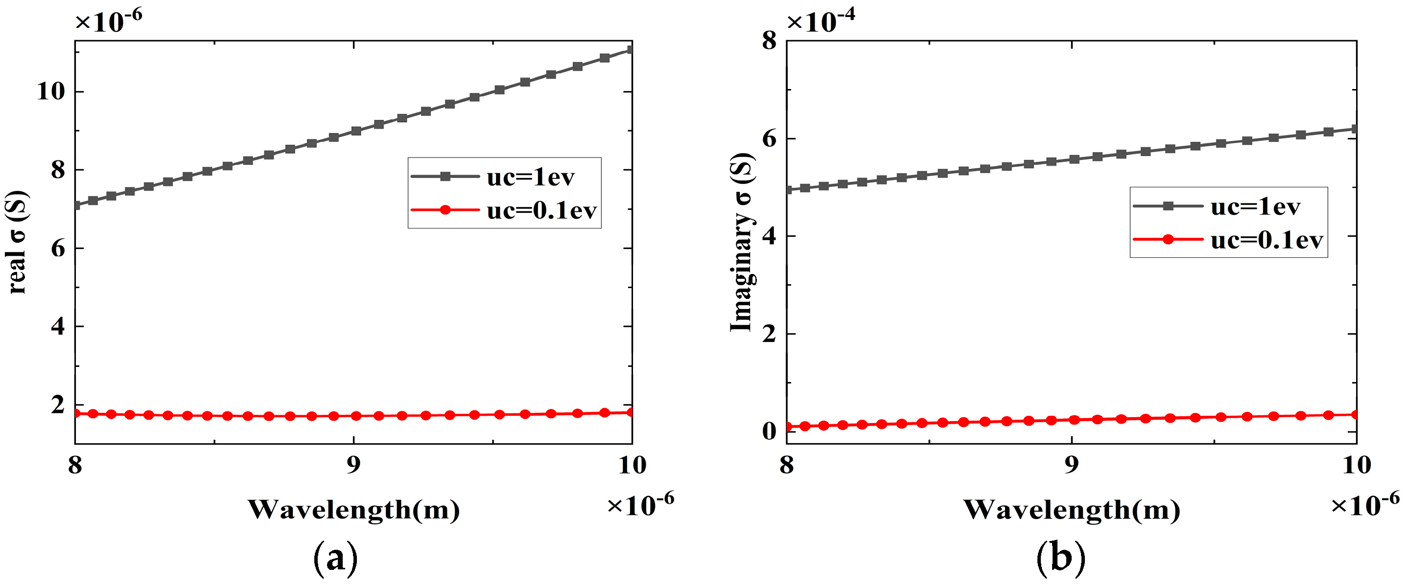
In this paper, the temperature T , scattering rate Γ , and operating wavelength λ are 300 K, 0.11 meV, and 9.3 μm, respectively. The relationship between graphene conductivity on chemical potential and wavelength is shown in Figure 2. The relationship between the chemical potential and the required external voltage is given by [53].
μ c v F π a 0 V e x t V D i r a c
where v F = 0.9 × 10 6 m/s is the Fermi velocity, V e x t is the external voltage applied to the graphene layer, V D i r a c is the natural doping-induced voltage shift, and a 0 = 9 × 10¹⁶ m−2·V−1 is a constant estimated from a single capacitor model [53]. Whenever the chemical potential of graphene changes, the dielectric constant of the structure also changes. The complex permittivity of graphene is expressed in terms of surface conductivity as follows [54].
ε = ε 0 I m σ ω Δ + i R e σ ω Δ
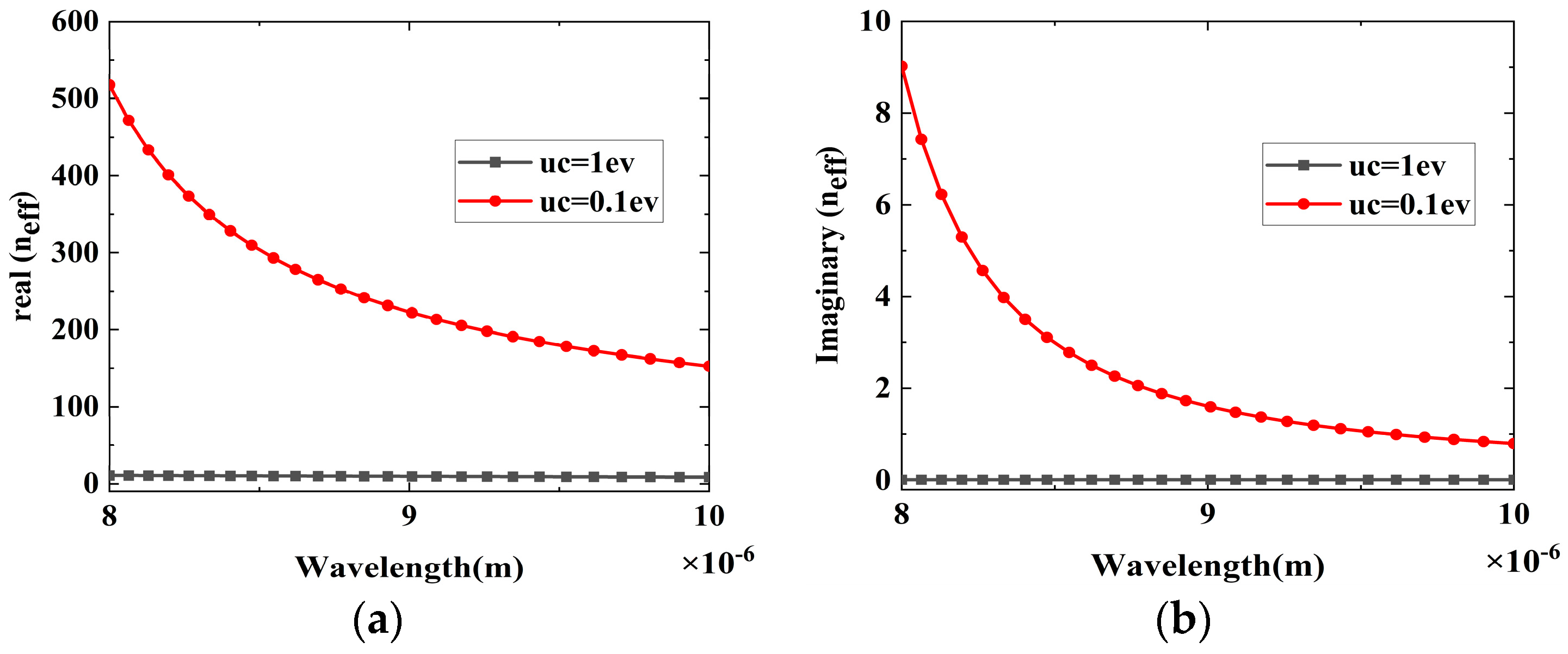
where ε 0 , Δ , R e σ , and I m σ are the free space permittivity, the effective thickness of the graphene layer, and the real and imaginary parts of the graphene conductivity, respectively. Similarly, the effective index ( n e f f ) of the structure changes when the chemical potential of graphene changes. Figure 3 shows the n e f f of a graphene layer surrounded by air. Therefore, the dielectric constant of graphene as well as the n e f f of the structure depends on the chemical potential of graphene.
Usually, when the chemical potential decreases, the imaginary part of n e f f increases, leading to higher losses and lower propagation lengths. This phenomenon paves the way for the design of graphene-based plasma switches. The wavelength (λSPP) and the propagation length (LSPP) of the SPP depend on the effective refractive index and are obtained by the following equation [17]:
λ S P P = λ 0 R e n e f f
L S P P = λ 0 2 π I m n e f f
For a single graphene layer surrounded by air, the effective refractive index of the TM wave at λ = 9.3 μm is 9.2712 + 0.0153i when the chemical potential is 1 Ev, which results in λSPP = 1.003 μm and LSPP = 96.74 μm. In addition, when the chemical potential is 0.1 Ev, the effective refractive index is 194.38 + 1.23i, which causes the SPP to propagate at λSPP = 0.048 μm and LSPP = 1.20 μm.The higher the real part of n e f f , the smaller the λSPP. In addition, by decreasing the imaginary part of n e f f , LSPP increases. Figure 4 shows the distribution of the z-component of the electric field at 0.1 Ev and 1 Ev chemical potential. When the chemical potential is 1 Ev, the SPP can propagate to the output port (“ON” state). In addition, when the chemical potential becomes 0.1 Ev, the SPP is not allowed to propagate (“OFF” state) and a large number of waves are reflected. It can be seen that when the chemical potential changes from 1 Ev to 0.1 Ev, the λSPP increases while the LSPP decreases severely. This behavior suggests that a graphene-based plasma switch can be designed by applying an external voltage.

2.2. The Proposed 4 × 2 Encoder

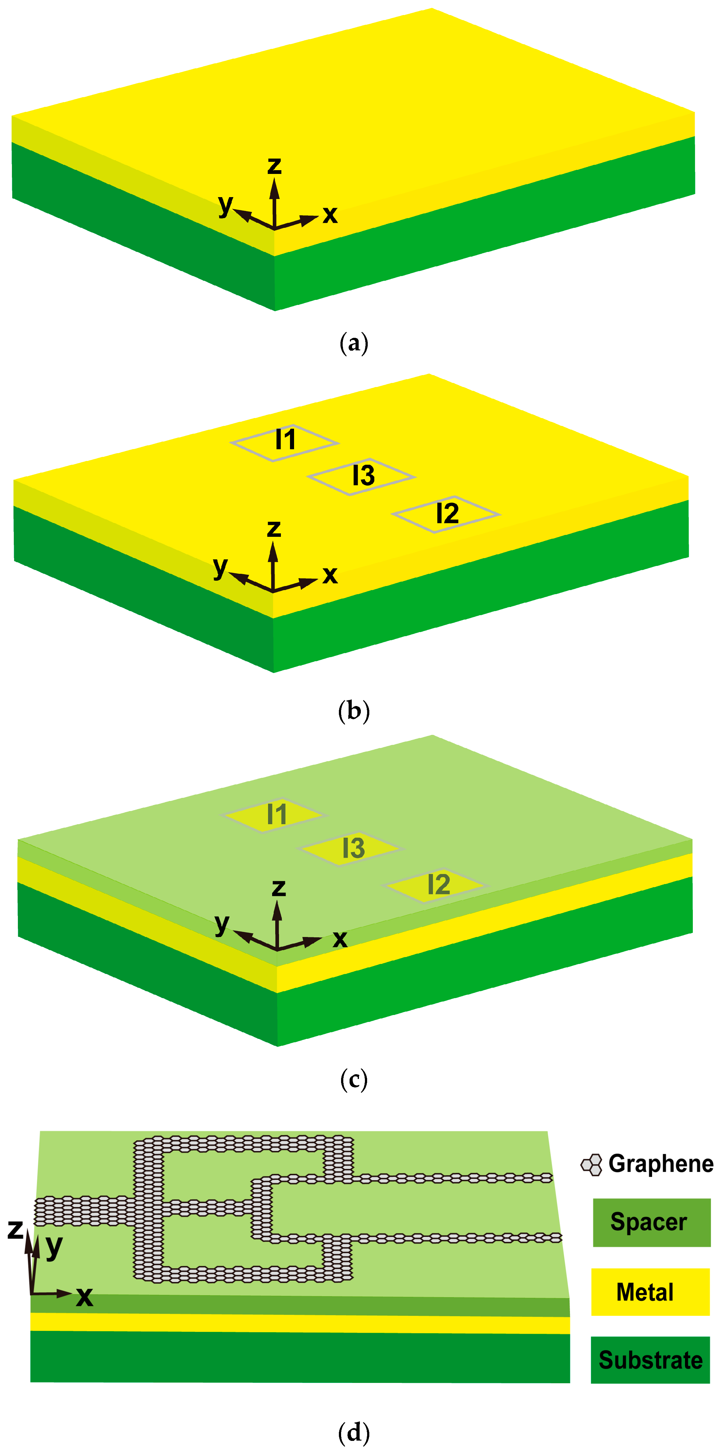
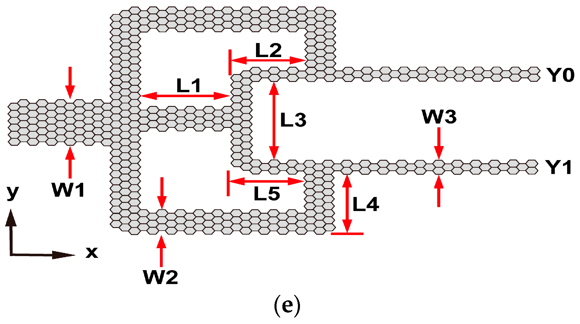
The basic structure schematic for implementing a graphene-based SPPs electro-optical 4 × 2 encoder is shown in Figure 5. Au of 30 nm thickness is deposited on the dielectric substrate. A review of the literature shows that gold is more effective than other metallic materials [55]. This metal layer can be used as a selective contact for applying external voltages while increasing the light confinement in the spacer layer. A dielectric layer of 20 nm thickness is located on the metal layer as a spacer layer, and graphene nanoribbons are deposited on the spacer layer. The dielectric layer has a dielectric constant of 1.4. The geometry of the graphene nanoribbon is shown in Figure 5e. Figure 5 illustrates the feasible fabrication process of the proposed 4 × 2 encoder. First, the metal layer is deposited on the dielectric substrate by electron beam evaporation (Figure 5a) [56]. Metal nanopick contacts can be produced by standard photolithography and wet etching (Figure 5b) [57]. Then, the spacer layer is deposited on top of the patterned metal layer and polished to obtain a thick surface with the desired thickness (Figure 5c). Finally, the graphene nanoribbons grown on copper are transferred to the spacer layer by employing a wet transfer method (Figure 5d) [58]. Combining graphene with metal makes the wave number of plasmonic wave modes increase, thus further enhancing the plasmonic waveguide confinement [59]. The graphene-based waveguide can support two modes, including an edge mode and a waveguide mode [60]. For low-width graphene nanoribbons, the waveguide is in single mode and only supports the edge mode. In this mode, the power is concentrated at the edges of the graphene layers. When the width of the graphene nanoribbon increases, the higher-order modes are also excited and the waveguide becomes multimode. To maximize the transmission [61], the widths of the graphene nanoribbons were chosen to be W1 = 100 nm, W2 = 45 nm, and W3 = 20 nm. Figure 6a shows the normalized total transmission coefficients of the three output branches G_U, G_D, and G_M as a function of W2 for an input width W1 = 100 nm at a wavelength of 9.3 µm. Due to the symmetry of the graphene structure, the G_U and G_D normalized total transmission coefficients are nearly equal. To further illustrate the selection of the optimal width W2, define K = T G _ U T G _ M T G _ U + T G _ D + T G _ M , as shown in Figure 6b; if the value of K is closer to 0, this means that the width of W2 is selected more reasonably, and vice versa, it means that the selection of W2 is not reasonable. It is clear from Figure 6a,b that the total transmission coefficient of each branch of the three-branch graphene structure is most similar when W2 is taken to be 45 nm. Figure 6c shows the total transmission coefficient of the electro-optical 4 × 2 encoder Y0 as a function of L2 at a wavelength of 9.3 µm with only the selective contact I1 in the on state. Similarly, when only the selective contact I2 is in the on state, the total transmission coefficient results are the same as those in Figure 6c, due to the symmetry of the structure. Figure 6d shows the total transmission coefficient of the electro-optical 4 × 2 encoder Y0 as a function of L2 at a wavelength of 9.3 µm with only the selective contact I3 in the on state. Similarly, due to the symmetry of the structure, the total transmission coefficient of Y1 is the same as that of Y0 at this time, and the total transmission coefficient of Y0 is used as a reference for the comparison of Figure 6c,d. Obviously, from Figure 6a,b, the total transmission coefficient of the output can be taken as the best value when L2 is around 157 nm and only one of the selected contacts I1, I2, and I3 is opened. This also indirectly shows that a small error in the graphene waveguide structure of the electro-optical 4 × 2 encoder due to the manufacturing process will not affect the function of the plasma electro-optical 4 × 2 encoder. By applying an external voltage to the selector contact, the chemical potential of the graphene layer is changed and the light can be propagated through the waveguide or blocked by using the properties of the graphene plasma switch. By adjusting the selector contact voltage to keep the chemical potential at 1 eV, the SPP can propagate within the boundary of the graphene dielectric layer and indicate a logical “1” state (“ON” state). In addition, when the chemical potential changes to 0.1 eV, the SPP propagation distance decreases significantly and indicates a logical “0” state (“OFF” state).
Figure 5. (a) Deposition of the metal layer on the dielectric substrate. (b) Process of patterning the selected contact electrodes to form the input electrode. (c) Deposition of the spacer layer on the patterned metal layer. (d) Transfer of graphene nanoribbons on top of the spacer layer and realization of the proposed 4 × 2 encoder. (e) Top view of the graphene waveguide. The geometric parameters are shown in Table 1. The dimensions are not to scale.
Photonics 10 00216 g005aPhotonics 10 00216 g005b
The working principles of the 4 × 2 encoder are as follows:
(1)
The chemical potential of the input electrodes in the three selective contact regions of the graphene layer can be changed. Each region acts as a switch.
(2)
The propagation of SPP in each input waveguide depends on the voltage applied to each switching electrode.
(3)
When any one of I1, I2, and I3 is ON, the state of I0 is logic “0”.
(4)
When I1 is ON, I2 and I3 are OFF.
(5)
When I2 is ON, I1 and I3 are OFF.
(6)
When I3 is ON, I1 and I2 are OFF.
(7)
When I1, I2, and I3 are OFF, it means I0 is in the logic “1” state.
Under this condition, the electro-optical 4 × 2 encoder is implemented. The truth table of the proposed 4 × 2 encoder is given in Table 2.

3. Results and Discussion

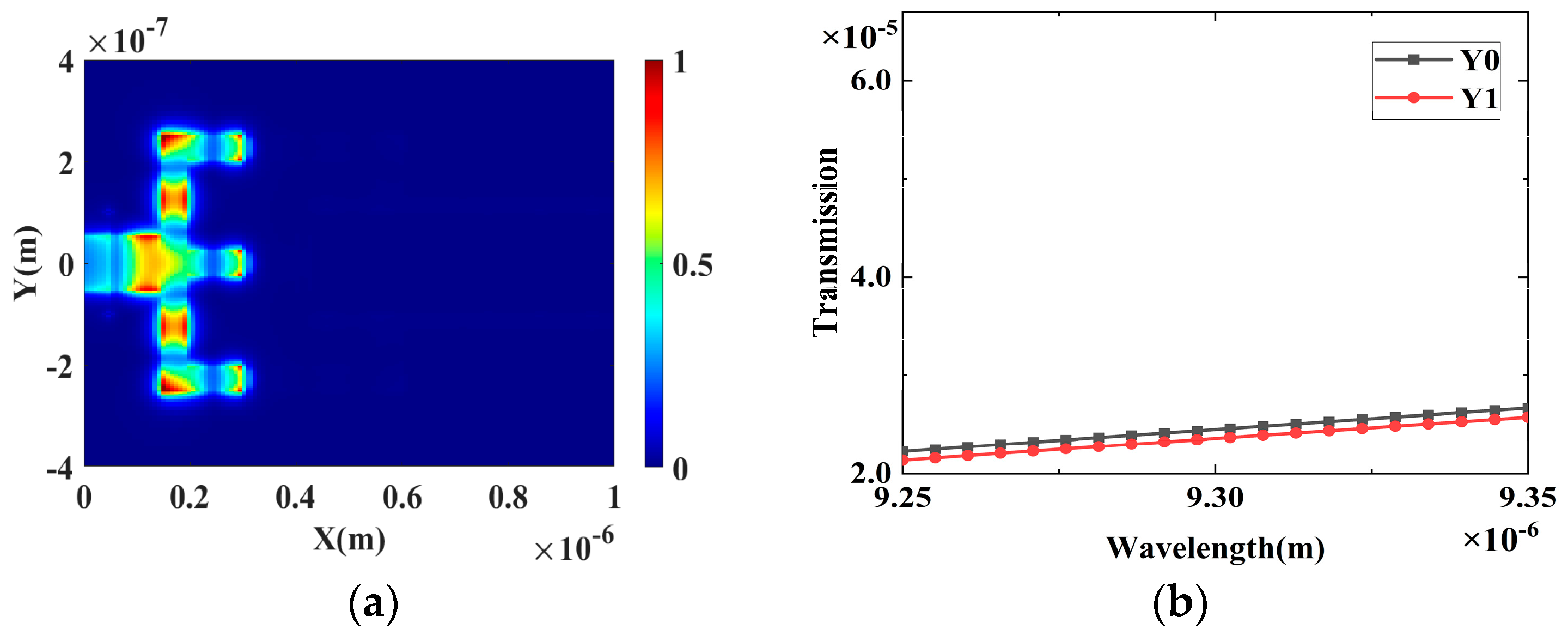
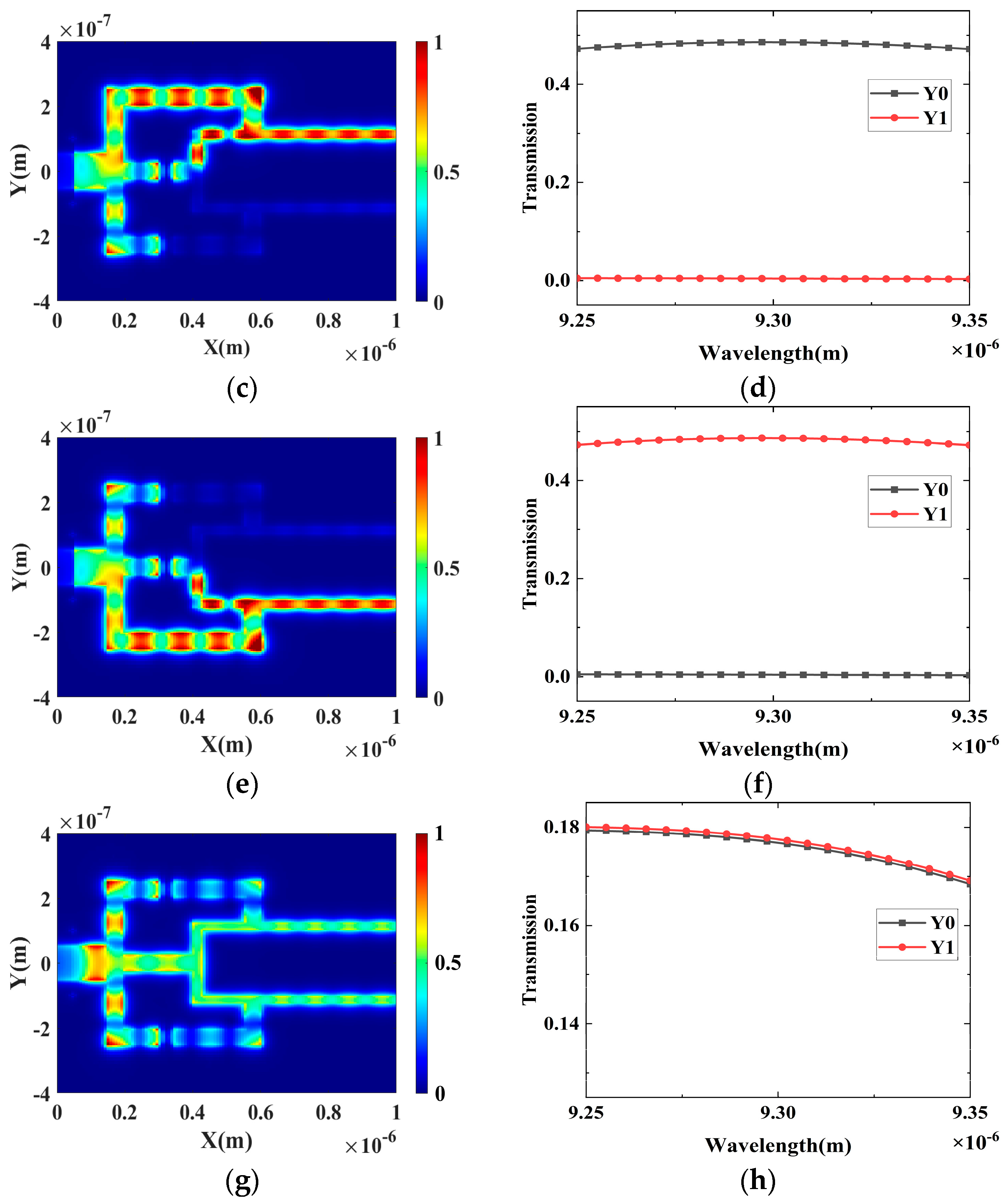
The proposed optoelectronic 4 × 2 encoder was simulated using the three-dimensional finite-dimensional time-domain difference (FDTD) method from Lumerical Solutions Canada, version 2020 R2. Compared to the spectral element method (SEM) [62], which focuses more on the mechanism, FDTD is more convenient for visualizing the electric field intensity distribution of the proposed structure. In the simulation, the grid size in the z-direction around the graphene layer is fixed at 0.1 nm and gradually increases outside the graphene layer. In addition, the grid sizes in the x and y directions are set to 8 nm and 4 nm, respectively. In addition, a perfectly matched layer (PML) boundary condition is used in the simulation. The structure is also excited by TM mode light waves with a wavelength of 9.3 μm and a bandwidth of 0.1 μm. Figure 7 shows the intensity of the electric field distribution for different encoding states. Different external voltages are applied to the plasma switches on the optical waveguide branches according to the selective contacts to characterize the four-bit code. The applied external voltage is 1 ev in the branch where the graphene plasma switch is located, and then I1, I2, and I3 are in the “ON” state and are defined as code “1”. Similarly, the applied external voltage is 0.1 ev in the branch where the graphene plasma switch is located, and the branch where I1, I2, and I3 are located is “OFF” and is defined as code “0”. In this way, when the plasma switch on the waveguide branch is coded “1”, the optical signal can be passed through the waveguide branch. According to the working principle of Section 3 and the true value of Table 2, the coding function of 4 × 2 is realized. As shown in Figure 7a, when I1, I2, and I3 are “OFF”, the default I0 is “ON”, and the four-bit coding flag is defined as “1000 “(I0 I1 I2 I3 I4). As there are no light signals in the output of Y0 and Y1, the 2-bit outputs is are“00” (Y0Y1). Figure 7c is the electric field intensity distribution, when only I1 is “ON”. Figure 7e is the electric field intensity distribution, when only I2 is “ON”. Figure 7g is the electric field intensity distribution, when only I3 is “ON”. Table 3 summarizes the normalized transmission under different coding conditions, which leads to two important parameters for the evaluation of the encoder.
In order to have a criterion to evaluate the coding performance, the parameter of the minimum extinction ratio ( E R m i n ) is defined as follows [63]:
E R m i n = 10 log T 1 , m i n T 0 , m a x
Here, T 1 , m i n is the minimum normalized transmission for the logic gate logic “1” state, while T 0 , m a x is the maximum normalized transmission for the logic gate logic “0” state. In addition, the modulation depth (MD) can be found in Refs [64,65].
M D m a x = T 1 , m a x T 0 , m i n T 1 , m a x
Here, T 1 , m a x is the maximum normalized transmission in the logic gate logic “1” state, while T 0 , m i n is the minimum normalized transmission in the logic gate logic “0” state. Table 4 summarizes the minimum extinction ratio and the maximum modulation depth for different encoding conditions. In order to evaluate the proposed encoder, the area, minimum extinction ratio, and maximum modulation depth are compared with the other optical encoders in Table 5. References [31,32,33,34,35,36,37,38,39,40,41] are all-optical and do not have the ability to adjust the transmission after fabrication, while in the proposed structure, the light transmission through the waveguide can be controlled by applying an appropriate voltage to the graphene layer and changing the chemical potential. In addition, the area of the proposed structure is small compared to other structures. Table 5 shows that the minimum extinction ratio of the designed encoder is greater than that of the references [31,32,33,34,35,36,37,38,39,40,41,42,43,44,45,46]. Thus, the small size and high extinction ratio are the main advantages of the device and guarantee the capability of the designed encoder in optical circuit applications.

4. Conclusions

A graphene-based plasmonic electro-optical 4 × 2 encoder at THz frequency has been designed and analyzed. The proposed plasmonic subwavelength structure in a graphene–insulator–metal (GIM) configuration has the advantages of optical properties such as the ultra-compact size, high brightness, high extinction ratio, and voltage dependence of the device. The structure achieves the desired encoding logic operation by applying different external voltages to the selector contact input electrode and thus varying the voltage of the graphene plasma switch. The minimum encoding extinction ratio and maximum modulation depth of the proposed electro-optical 4 × 2 encoder are 37 dB and 99.99%, respectively, with a structure area of 0.8 μm2. The results show that the proposed plasmonic encoder can be used in optical integrated circuits. In addition, the reversible design of the electro-optical 4 × 2 encoder based on graphene plasma proposed in this paper will be the next research focus.

Author Contributions

Conceptualization and model, A.Z.; numerical simulation, A.Z. and P.B.; writing—original draft preparation, A.Z. and P.B.; investigation and formal analysis C.H.; writing—review and editing, A.Z., P.B. and J.N.; project administration and resources, R.M. All authors have read and agreed to the published version of the manuscript.

Funding

This work was partially funded by the National Natural Science Foundation of China (62161008, 61861012), the Guangxi Natural Science Foundation Joint Funding Project (2018GXNSFAA138115), and the Guangxi Key Laboratory of Automatic Detecting Technology and Instruments (YQ22110).

Institutional Review Board Statement

Not applicable.

Informed Consent Statement

Not applicable.

Data Availability Statement

The data supporting the findings of this study are available within the article.

Conflicts of Interest

The authors declare no conflict of interest.

References

  1. Davis, T.J.; Gómez, D.E.; Roberts, A. Plasmonic circuits for manipulating optical information. Nanophotonics 2016, 6, 543–559. [Google Scholar] [CrossRef]
  2. Athale, R.; Psaltis, D. Optical computing: Past and future. Opt. Photonics News 2016, 27, 32. [Google Scholar] [CrossRef]
  3. Wei, H.; Wang, Z.; Tian, X.; Käll, M.; Xu, H. Cascaded logic gates in nanophotonic plasmon networks. Nat. Commun. 2011, 2, 387. [Google Scholar] [CrossRef] [PubMed] [Green Version]
  4. Birr, T.; Zywietz, U.; Chhantyal, P.; Chichkov, B.N.; Reinhardt, C. Ultrafast surface plasmon-polariton logic gates and half-adder. Opt. Express 2015, 23, 31755. [Google Scholar] [CrossRef] [PubMed]
  5. Hardy, J.; Shamir, J. Optics inspired logic architecture. Opt. Express 2015, 15, 150. [Google Scholar] [CrossRef]
  6. Cutrona, L.; Leith, E.; Palermo, C.; Porcello, L. Optical data processing and filtering systems. IEEE Trans. Inf. Theory 1960, 6, 386–400. [Google Scholar] [CrossRef]
  7. Ambs, P. Optical computing: A 60-year adventure. Adv. Opt. Technol. 2010, 2010, 1–15. [Google Scholar] [CrossRef] [Green Version]
  8. Gayen, D.K.; Bhattachryya, A.; Chattopadhyay, T.; Roy, J.N. Ultrafast all-optical half adder using quantum-dot semiconductor optical amplifier-based mach-zehnder interferometer. J. Light. Technol. 2012, 30, 3387–3393. [Google Scholar] [CrossRef]
  9. Rezaei, M.H.; Zarifkar, A. Subwavelength electro-optical half-subtractor and half-adder based on graphene plasmonic waveguides. Plasmonics 2019, 14, 1939–1947. [Google Scholar] [CrossRef]
  10. Huang, B.-H.; Lu, W.-B.; Li, X.-B.; Wang, J.; Liu, Z. Waveguide-coupled hybrid plasmonic modulator based on graphene. Appl. Opt. 2019, 55, 5598. [Google Scholar] [CrossRef]
  11. Bai, C.; Chen, J.; Zhang, Y.; Zhang, D.; Zhan, Q. Dynamic tailoring of an optical skyrmion lattice in surface plasmon polaritons. Opt. Express 2020, 28, 10320. [Google Scholar] [CrossRef] [PubMed]
  12. Hosseini, A.; Massoud, Y. A low-loss metal-insulator-metal plasmonic bragg reflector. Opt. Express 2006, 14, 11318. [Google Scholar] [CrossRef] [PubMed]
  13. Chen, J.; Smolyakov, G.A.; Brueck, S.R.; Malloy, K.J. Surface plasmon modes of finite, planar, metal-insulator-metal plasmonic waveguides. Opt. Express 2008, 16, 14902. [Google Scholar] [CrossRef] [PubMed] [Green Version]
  14. Fitrakis, E.P.; Kamalakis, T.; Sphicopoulos, T. Slow light in insulator–metal–insulator plasmonic waveguides. J. Opt. Soc. Am. B 2011, 28, 2159. [Google Scholar] [CrossRef]
  15. Gupta, R.; Dyer, M.J.; Weimer, W.A. Preparation and characterization of surface plasmon resonance tunable gold and silver films. J. Appl. Phys. 2002, 92, 5264–5271. [Google Scholar] [CrossRef]
  16. Luo, X.; Qiu, T.; Lu, W.; Ni, Z. Plasmons in graphene: Recent progress and applications. Mater. Sci. Eng. R Rep. 2013, 74, 351–376. [Google Scholar] [CrossRef] [Green Version]
  17. Rezaei, M.H.; Zarifkar, A.; Miri, M. Ultra-compact electro-optical graphene-based plasmonic multi-logic gate with high extinction ratio. Opt. Mater. 2018, 84, 572–578. [Google Scholar] [CrossRef]
  18. Kazanskiy, N.L.; Khonina, S.N.; Butt, M.A.; Kaźmierczak, A.; Piramidowicz, R. A numerical investigation of a plasmonic sensor based on a metal-insulator-metal waveguide for simultaneous detection of biological analytes and ambient temperature. Nanomaterials 2021, 11, 2551. [Google Scholar] [CrossRef] [PubMed]
  19. Khatir, M.; Granpayeh, N. An exact analysis method of SPP propagation in the anisotropic magneto-optic slab waveguides: I. Transversal configuration. Optik 2013, 124, 276–281. [Google Scholar] [CrossRef]
  20. Thomas, R.; Ikonic, Z.; Kelsall, R.W. Electro-optic metal–insulator–semiconductor–insulator–metal Mach-Zehnder plasmonic modulator. Photonics Nanostruct. Fundam. Appl. 2012, 10, 183–189. [Google Scholar] [CrossRef]
  21. Heydari, M.B.; Samiei, M.H.V. Analytical study of tm-polarized surface plasmon polaritons in nonlinear multi-layer graphene-based waveguides. Plasmonics 2021, 16, 841–848. [Google Scholar] [CrossRef]
  22. Ye, L.; Sui, K.; Liu, Y.; Zhang, M.; Liu, Q.H. Graphene-based hybrid plasmonic waveguide for highly efficient broadband mid-infrared propagation and modulation. Opt. Express 2018, 26, 15935. [Google Scholar] [CrossRef] [PubMed] [Green Version]
  23. Liu, J.; Khan, Z.U.; Wang, C.; Zhang, H.; Sarjoghian, S. Review of graphene modulators from the low to the high figure of merits. J. Phys. D Appl. Phys. 2020, 53, 233002. [Google Scholar] [CrossRef]
  24. Rezaei, M.H.; Shiri, M. High-performance tunable resonant electro-optical modulator based on suspended graphene waveguides. Opt. Express 2021, 29, 16299. [Google Scholar] [CrossRef] [PubMed]
  25. Liang, W.; Li, Z.; Wang, Y.; Chen, W.; Li, Z. All-angle optical switch based on the zero reflection effect of graphene–dielectric hyperbolic metamaterials. Photonics Res. 2019, 7, 318. [Google Scholar] [CrossRef]
  26. Ghorbanzadeh, M.; Darbari, S.; Moravvej-Farshi, M.K. Graphene-based plasmonic force switch. Appl. Phys. Lett. 2016, 108, 111105. [Google Scholar] [CrossRef]
  27. Jiang, Y.; Laurenciu, N.C.; Wang, H.; Cotofana, S.D. Graphene nanoribbon based complementary logic gates and circuits. IEEE Trans. Nanotechnol. 2019, 18, 287–298. [Google Scholar] [CrossRef] [Green Version]
  28. Wu, X.; Tian, J.; Yang, R. A type of all-optical logic gate based on graphene surface plasmon polaritons. Opt. Commun. 2017, 403, 185–192. [Google Scholar] [CrossRef]
  29. Nag, A.; Mitra, A.; Mukhopadhyay, S.C. Graphene and its sensor-based applications: A review. Sens. Actuators A Phys. 2018, 270, 177–194. [Google Scholar] [CrossRef]
  30. Tian, W.; Liu, X.; Yu, W. Research progress of gas sensor based on graphene and its derivatives: A review. Appl. Sci. 2018, 8, 1118. [Google Scholar] [CrossRef] [Green Version]
  31. Hadadan, F.; Soroosh, M. A new proposal for 4-to-2 optical encoder using nonlinear photonic crystal ring resonators. Int. J. Opt. Photonics 2019, 13, 119–126. [Google Scholar] [CrossRef] [Green Version]
  32. Lee, K.Y.; Yang, Y.C.; Lin, Y.J.; Lee, W.Y.; Lee, C.C.; Wong, S.H. The designs of 4 × 2 encoder based on photonic crystals. Asia Commun. Photonics Conf. Exhib. 2009, 2009, 1–7. [Google Scholar]
  33. Mehdizadeh, F.; Soroosh, M.; Alipour-Banaei, H. Proposal for 4-to-2 optical encoder based on photonic crystals. IET Optoelectron. 2017, 11, 29–35. [Google Scholar] [CrossRef]
  34. Ouahab, I.; Naoum, R. A novel all optical 4 × 2 encoder switch based on photonic crystal ring resonators. Optik 2016, 127, 7835–7841. [Google Scholar] [CrossRef]
  35. Naghizade, S.; Khoshsima, H. Low Input Power an All Optical 4 × 2 Encoder based on Triangular Lattice Shape Photonic Crystal. J. Opt. Commun. 2018, 42, 17–24. [Google Scholar] [CrossRef]
  36. Hassangholizadeh-Kashtiban, M.; Sabbaghi-Nadooshan, R.; Alipour-Banaei, H. A novel all optical reversible 4 × 2 encoder based on photonic crystals. Optik 2015, 126, 2368–2372. [Google Scholar] [CrossRef]
  37. Seif-Dargahi, H. Ultra-fast all-optical encoder using photonic crystal-based ring resonators. Photonic Netw. Commun. 2018, 36, 272–277. [Google Scholar] [CrossRef]
  38. Moniem, T.A. All-optical digital 4 × 2 encoder based on 2D photonic crystal ring resonators. J. Mod. Opt. 2015, 63, 735–741. [Google Scholar] [CrossRef]
  39. Gholamnejad, S.; Zavvari, M. Design and analysis of all-optical 4–2 binary encoder based on photonic crystal. Opt. Quantum Electron. 2017, 49, 302. [Google Scholar] [CrossRef]
  40. Naghizade, S.; Saghaei, H. A novel design of all-optical 4 to 2 encoder with multiple defects in silica-based photonic crystal fiber. Optik 2020, 222, 165419. [Google Scholar] [CrossRef]
  41. Parandin, F. High contrast ratio all-optical 4 × 2 encoder based on two-dimensional photonic crystals. Opt. Laser Technol. 2019, 113, 447–452. [Google Scholar] [CrossRef]
  42. Alipour-Banaei, H.; Rabati, M.G.; Abdollahzadeh-Badelbou, P.; Mehdizadeh, F. Application of self-collimated beams to realization of all optical photonic crystal encoder. Phys. E Low-Dimens. Syst. Nanostruct. 2016, 75, 77–85. [Google Scholar] [CrossRef]
  43. Zhang, D.; You, G. Miniaturization design of all-optical encoder based on surface design and radiation source control. Phys. E Low-Dimens. Syst. Nanostruct. 2021, 127, 114469. [Google Scholar] [CrossRef]
  44. Latha, K.; Arunkumar, R.; Prabha, K.R.; Robinson, S. Performance Analysis of all Optical 4*2 and 8*3 Encoder Using Two Dimensional Photonic Crystals Waveguides. Silicon 2021, 14, 3245–3258. [Google Scholar] [CrossRef]
  45. Haddadan, F.; Soroosh, M.; Alaei-Sheini, N. Designing an electro-optical encoder based on photonic crystals using the graphene–Al2O3 stacks. Appl. Opt. 2020, 59, 2179. [Google Scholar] [CrossRef] [PubMed]
  46. Mohammad, R.R.; Mohammad, A.M. Design and simulation of wavelength demultiplexer based on heterostructure photonic crystals ring resonators. Phys. E Low-Dimens. Syst. Nanostruct. 2013, 50, 97–101. [Google Scholar]
  47. Mohammad, R.R.; Mohammad, A.M. High sensitivity plasmonic refractive index sensing and its application for human blood group identification. Sens. Actuators B Chem. 2017, 249, 168–176. [Google Scholar]
  48. Haddadan, F.; Soroosh, M.; Alaei-Sheini, N. Cross-talk reduction in a graphene-based ultra-compact plasmonic encoder using an Au nano-ridge on a silicon substrate. Appl. Opt. 2022, 61, 3209. [Google Scholar] [CrossRef]
  49. Fei, Z.; Rodin, A.S.; Andreev, G.O.; Bao, W.; McLeod, A.S.; Wagner, M.; Zhang, L.M.; Zhao, Z.; Thiemens, M.; Dominguez, G.; et al. Gate-tuning of graphene plasmons revealed by infrared nano-imaging. Nature 2012, 487, 82–85. [Google Scholar] [CrossRef] [Green Version]
  50. Koppens, F.H.L.; Chang, D.E.; García de Abajo, F.J. Graphene plasmonics: A platform for strong light–matter interactions. Nano Lett. 2011, 11, 3370–3377. [Google Scholar] [CrossRef] [Green Version]
  51. Rezaei, M.H.; Zarifkar, A. High-extinction ratio and ultra-compact two-bit comparators based on graphene-plasmonic waveguides. Appl. Opt. 2019, 58, 9829. [Google Scholar] [CrossRef] [PubMed]
  52. Farmani, A.; Zarifkar, A.; Sheikhi, M.H.; Miri, M. Design of a tunable graphene plasmonic-on-white graphene switch at infrared range. Superlattices Microstruct. 2017, 112, 404–414. [Google Scholar] [CrossRef]
  53. Liu, M.; Yin, X.; Ulin-Avila, E.; Geng, B.; Zentgraf, T.; Ju, L.; Wang, F.; Zhang, X. A graphene-based broadband optical modulator. Nature 2011, 474, 64–67. [Google Scholar] [CrossRef] [PubMed]
  54. Rezaei, M.H.; Zarifkar, A. Transmission characteristics of a graphene-based plasmonic decoder for thz applications. In Proceedings of the 2018 9th International Symposium on Telecommunications (IST), Tehran, Iran, 17–19 December 2018; p. 12. [Google Scholar]
  55. Rezaei, M.H.; Zarifkar, A. Realization of electro-optical decoder, half-adder, and half-subtractor using graphene plasmonic waveguides. Opt. Quantum Electron. 2021, 53, 297. [Google Scholar] [CrossRef]
  56. Gutruf, P.; Walia, S.; Nur Ali, M.; Sriram, S.; Bhaskaran, M. Strain response of stretchable micro-electrodes: Controlling sensitivity with serpentine designs and encapsulation. Appl. Phys. Lett. 2014, 104, 021908. [Google Scholar] [CrossRef]
  57. Caironi, M.; Noh, Y.-Y. Large Area and Flexible Electronics; John Wiley & Sons: Hoboken, NJ, USA, 2015. [Google Scholar]
  58. Li, P.; Chen, C.; Zhang, J.; Li, S.; Sun, B.; Bao, Q. Graphene-Based transparent electrodes for hybrid solar cells. Front. Mater. 2014, 1, 26. [Google Scholar] [CrossRef]
  59. Lin, I.T.; Lai, Y.P.; Wu, K.H.; Liu, J.M. Terahertz optoelectronic property of graphene: Substrate-induced effects on plasmonic characteristics. Appl. Sci. 2014, 4, 28–41. [Google Scholar] [CrossRef] [Green Version]
  60. Nikitin, A.Y.; Guinea, F.; García-Vidal, F.J.; Martín-Moreno, L. Edge and waveguide terahertz surface plasmon modes in graphene microribbons. Phys. Rev. B 2011, 84, 161407. [Google Scholar] [CrossRef] [Green Version]
  61. Zhu, X.; Yan, W.; Mortensen, N.A.; Xiao, S. Bends and splitters in graphene nanoribbon waveguides. Opt. Express 2013, 21, 3486. [Google Scholar] [CrossRef] [PubMed] [Green Version]
  62. Mahariq, I.; Kuzuoğlu, M.; Tarman, I.H.; Kurt, H. Photonic Nanojet Analysis by Spectral Element Method. IEEE Photonics J. 2014, 6, 1–14. [Google Scholar] [CrossRef]
  63. Safinezhad, A.; Babaei Ghoushji, H.; Shiri, M.; Rezaei, M.H. High-performance and ultrafast configurable all-optical photonic crystal logic gates based on interference effects. Opt. Quantum Electron. 2021, 53, 259. [Google Scholar] [CrossRef]
  64. Yarahmadi, M.; Moravvej-Farshi, M.K.; Yousefi, L. Subwavelength graphene-based plasmonic thz switches and logic gates. IEEE Trans. Terahertz Sci. Technol. 2015, 5, 725–731. [Google Scholar] [CrossRef]
  65. Rahm, M.; Li, J.S.; Padilla, W.J. THz wave modulators: A brief review on different modulation techniques. J. Infrared Millim. Terahertz Waves 2012, 34, 1–27. [Google Scholar] [CrossRef]
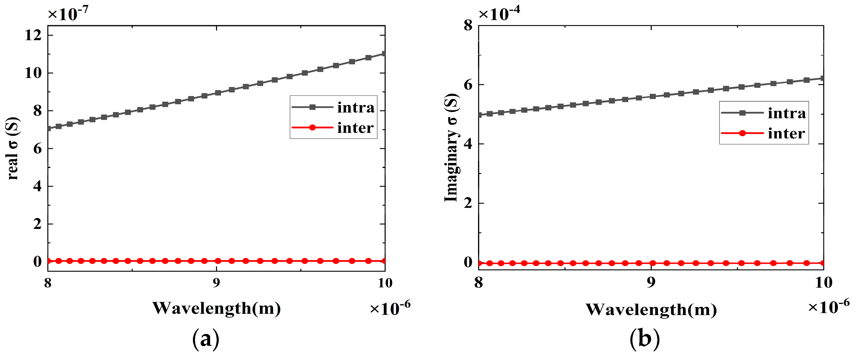
Figure 1. Real (a) and imaginary (b) parts of interband and intraband conductivity of graphene surface as a function of wavelength at μ c = 1 eV.
Photonics 10 00216 g001
Figure 2. Real part (a) and imaginary part (b) of graphene surface conductivity as a function of chemical potential at 8 μm < λ < 10 μm.
Photonics 10 00216 g002
Figure 3. Effective refractive index of graphene in the real part (a) and the imaginary part (b) as a function of chemical potential at 8 μm < λ < 10 μm.
Photonics 10 00216 g003
Figure 4. The real part of Ez for (a) μ c = 1 Ev and (b) μ c = 0.1 Ev. The dashed line indicates the position where the chemical potential of the graphene layer changes from 1 Ev to 0.1 Ev.
Photonics 10 00216 g004
Figure 6. W1 = 100 nm and λ = 9.3µm. (a) Normalized transmission coefficient of the three-branch graphene-based light splitter as a function of W2. (b) The value of K for the three-branch graphene-based light splitter as a function of W2. (c) When only I1 is “ON”, the transmission coefficient of Y0 at the output of the proposed 4 × 2 encoder as a function of L2. (d) The transmission coefficient of Y0 at the output of the proposed 4 × 2 encoder as a function of L2 when only I3 is “ON”. The inset illustrates the z-component of the electric field distribution confined within the dielectric layer.
Photonics 10 00216 g006
Figure 7. Electric field distribution of the proposed 4 × 2 encoder under different conditions: (a) I0 = 1 and I1 = I2 = I3 = 0, (c) I1 = 1 and I0 = I2 = I3 = 0, (e) I2 = 1 and I0 = I1 = I3 = 0, (g) I3 = 1 and I0 = I1 = I2 = 0, and their corresponding wavelengths as a function of the transmission spectrum at the output (b) Y0 = 0,Y1 = 0, (d) Y0 = 1,Y1 = 0, (f) Y0 = 1,Y1 = 0, and (h) Y0 = 1,Y1 = 1.
Photonics 10 00216 g007aPhotonics 10 00216 g007b
Table 1. Table of graphene pattern layer geometries (nm).
W1W2W3L1L2L3L4L5
1004520205157210125157
Table 2. Truth table of the proposed 4 × 2 encoder.
InputOutput
I0I1I2I3Y0Y1
100000
010010
001001
000111
Table 3. Normalized transmission under different coding conditions.
InputOutput
I0I1I2I3Y0Y1
10002.69389 × 10−52.69155 × 10⁻⁵
01000.4835410.00436279
00100.004366110.483586
00010.1766010.176639
Table 4. Minimum ER of the proposed 4 × 2 encoder logic gate.
InputMinimum ER (dB)Maximum MD (%)
I0I1I2I3
1000~~
010047.072699.99
001047.073699.99
000137.000299.98
Table 5. Comparison of the obtained results with other works.
DescriptionER (dB)MD (%)Area (μm2)Ref
Nonlinear PhC16.3398.04612[33]
PhC7.3294.90880[34]
PhC12.9291.38~[35]
PhC ring resonators9.54~757[36]
Triangular lattice shape PhC11.7696.84723[37]
PhC9.03~200[38]
PhC ring resonators9.2489.94792[39]
2D PhC ring resonators~99.491225[40]
PhC17.78~744[41]
Silica-based PhC fiber13.7697.78150[42]
2D PhC16.5397.80132.7[43]
PhC using the graphene–Al2O3 stacks7.691127[45]
Graphene-based plasmonic using Au nano-ridge14.44~0.36[48]
Graphene plasmonic waveguides3799.990.8This work
Disclaimer/Publisher’s Note: The statements, opinions and data contained in all publications are solely those of the individual author(s) and contributor(s) and not of MDPI and/or the editor(s). MDPI and/or the editor(s) disclaim responsibility for any injury to people or property resulting from any ideas, methods, instructions or products referred to in the content.