Tailoring the Direct Current Modulation Response of Electrically Pumped Semiconductor Nano-Laser Arrays


Abstract
:1. Introduction
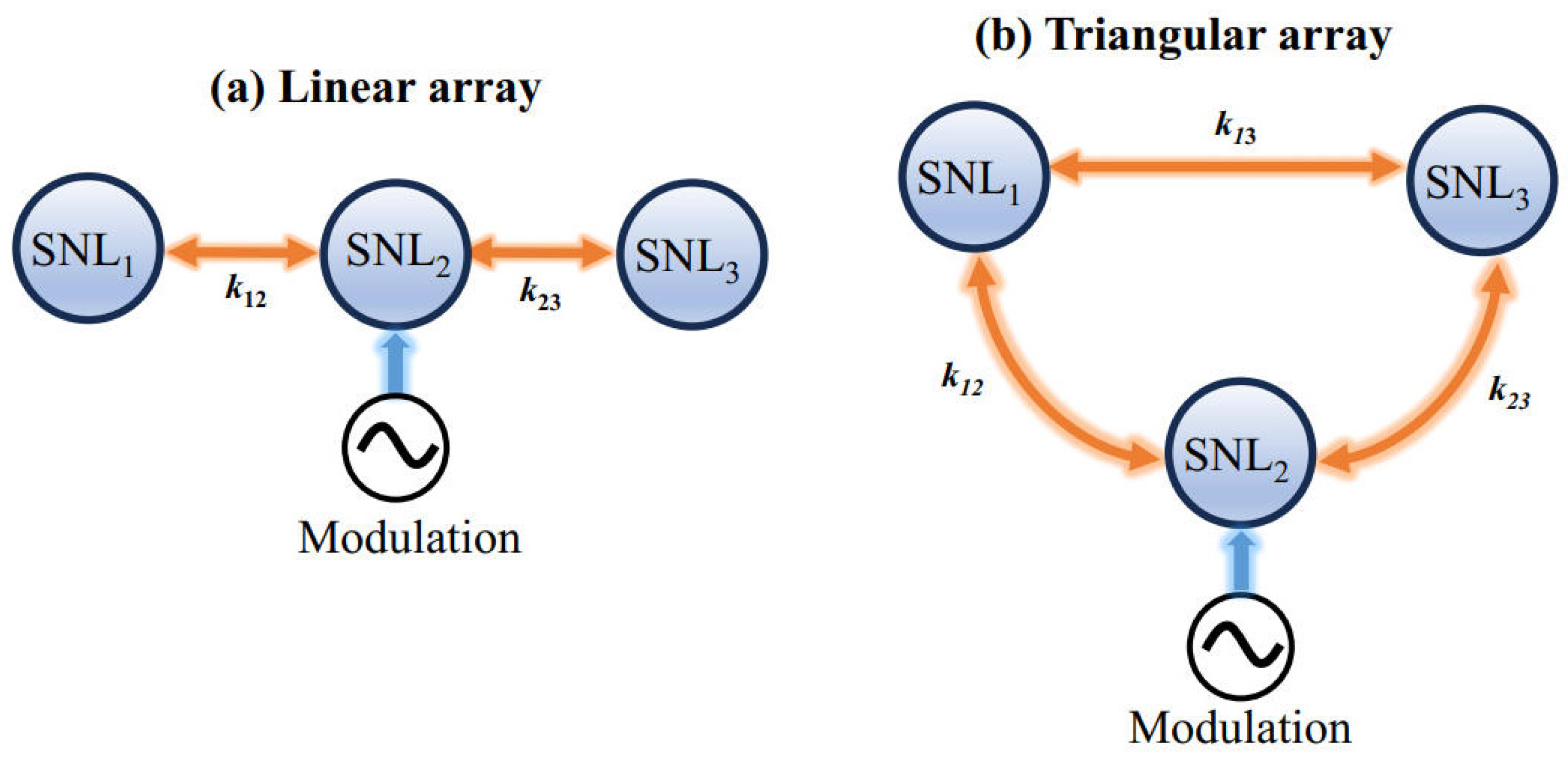
2. Model
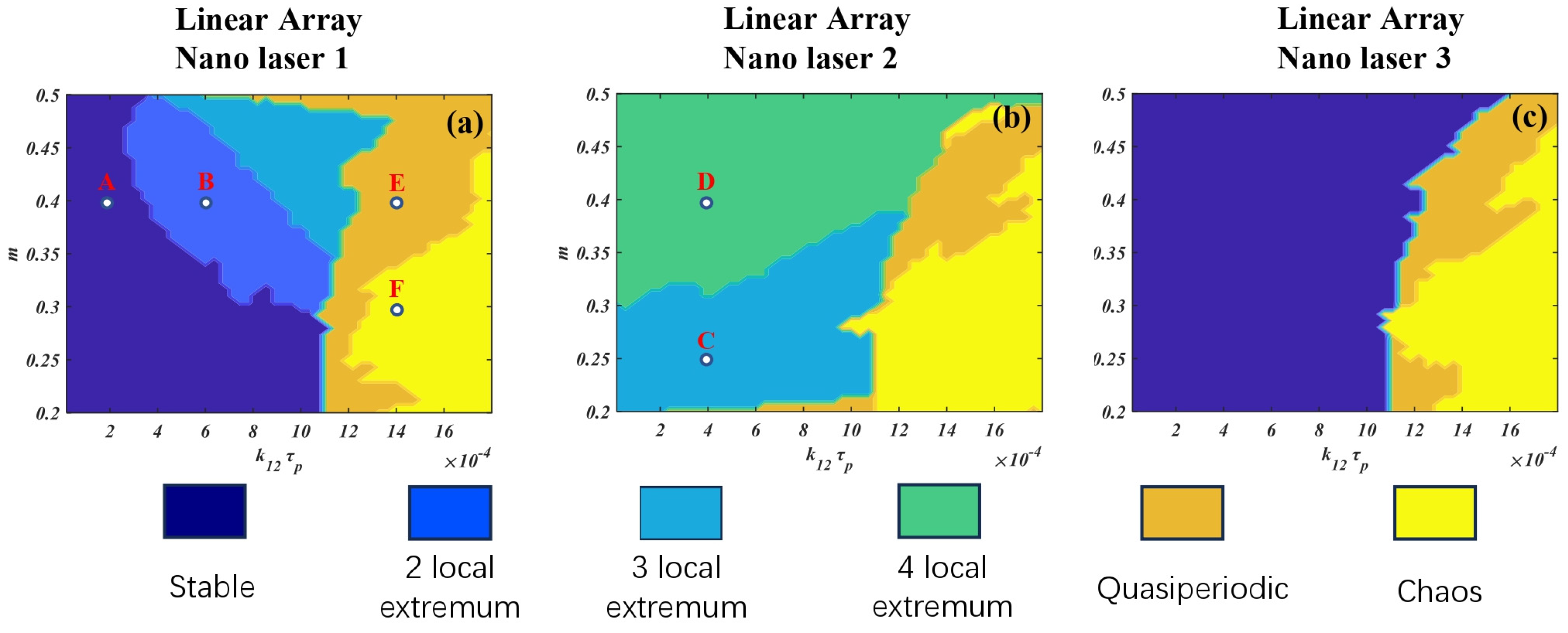
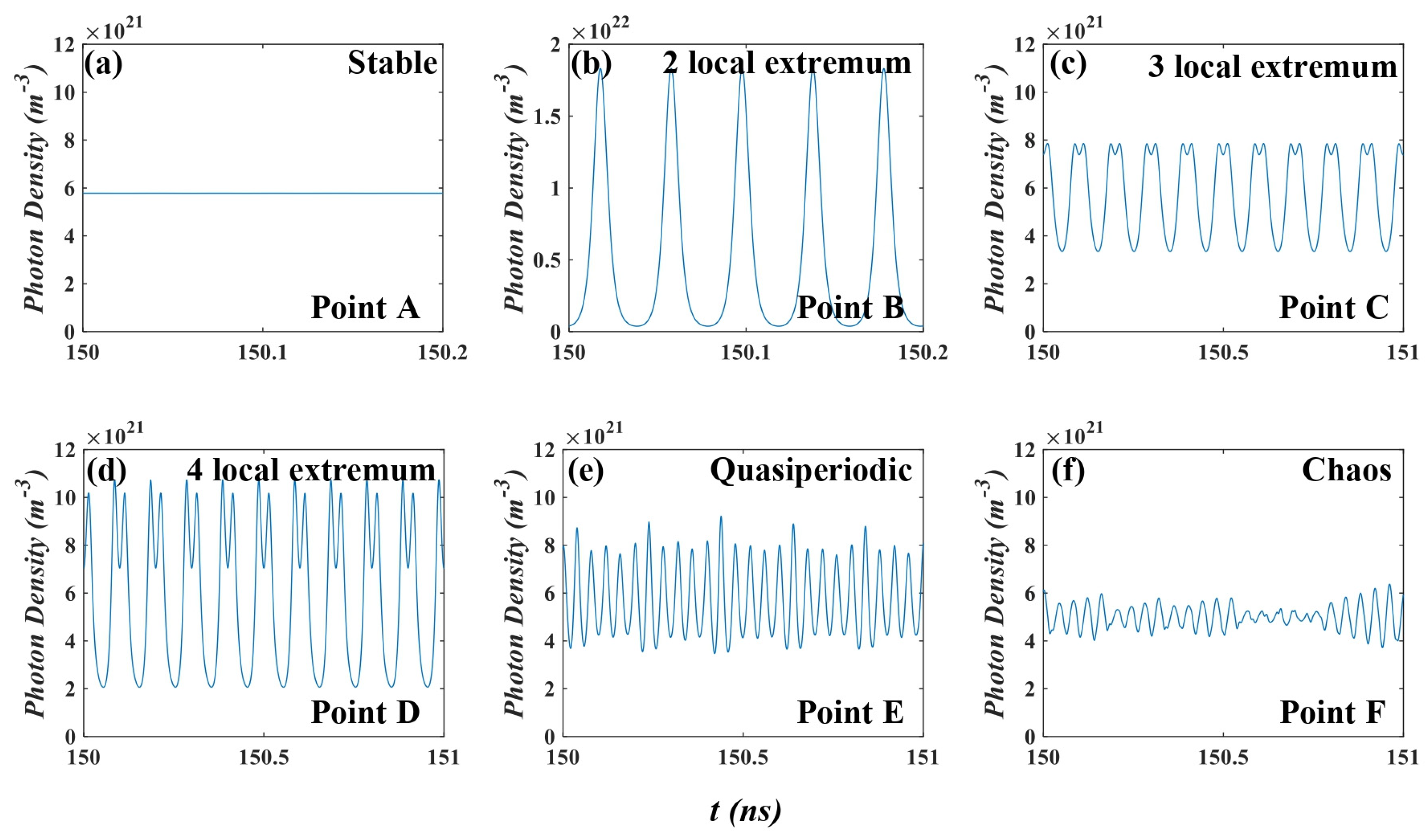
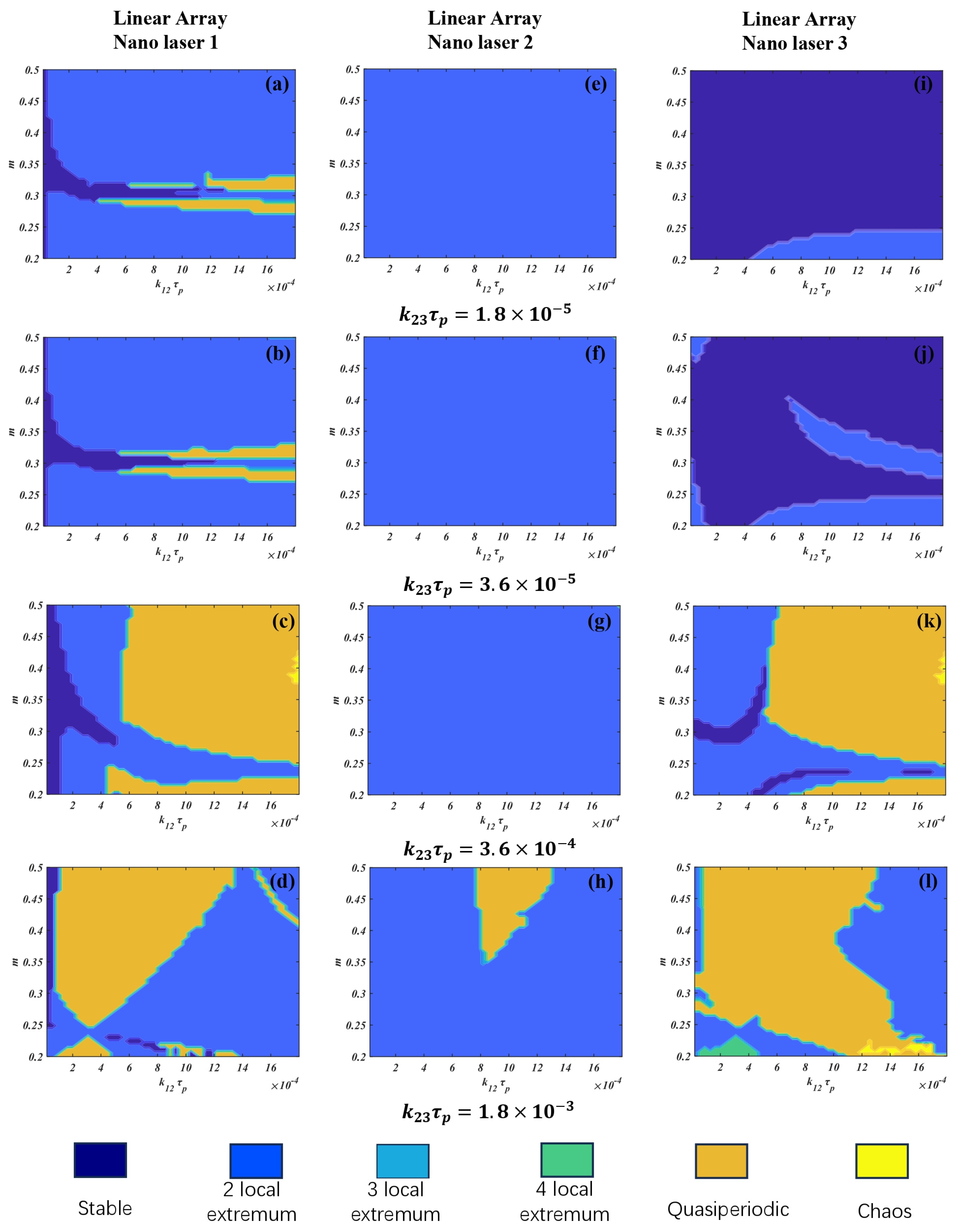
3. Results
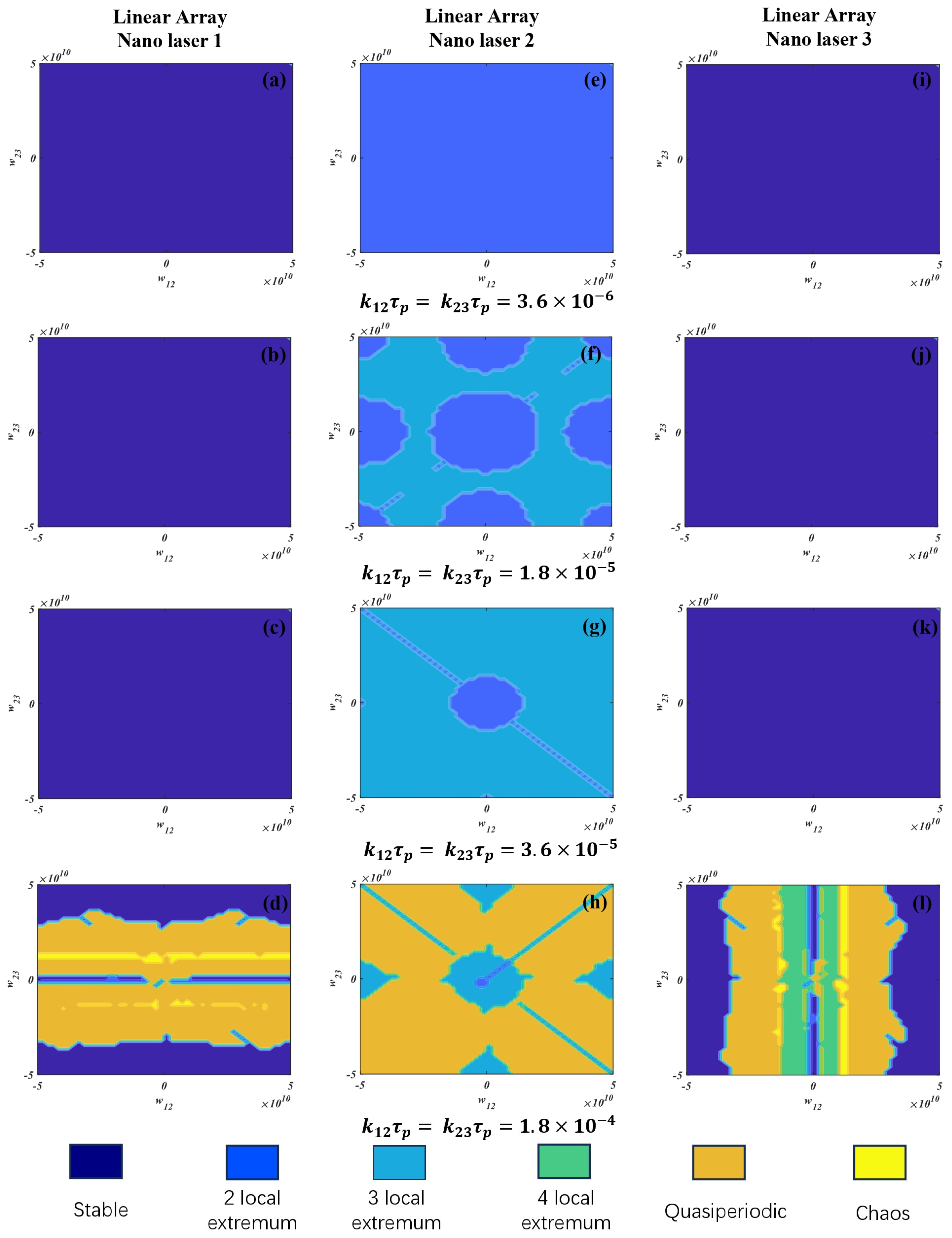
3.1. Linear Array
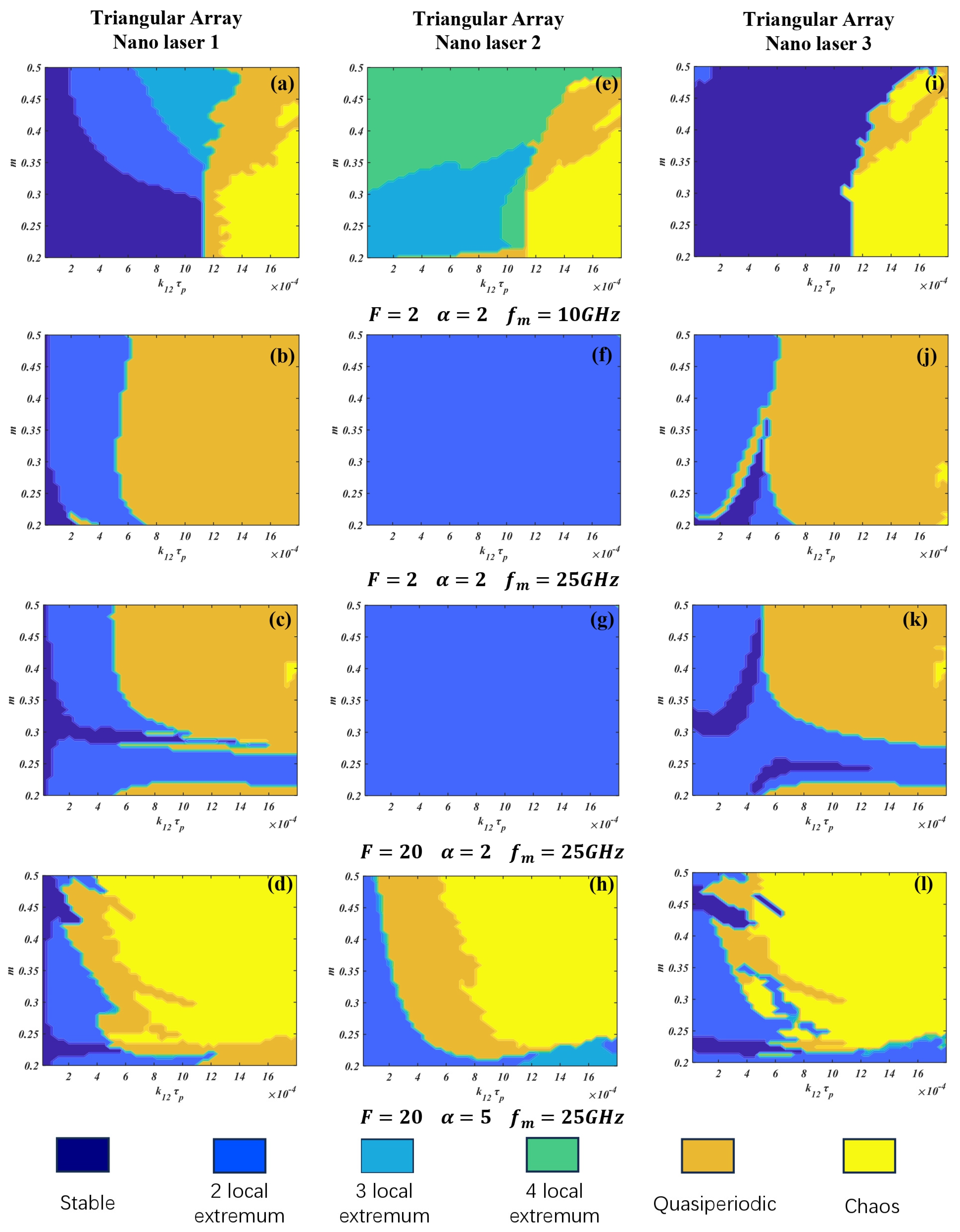
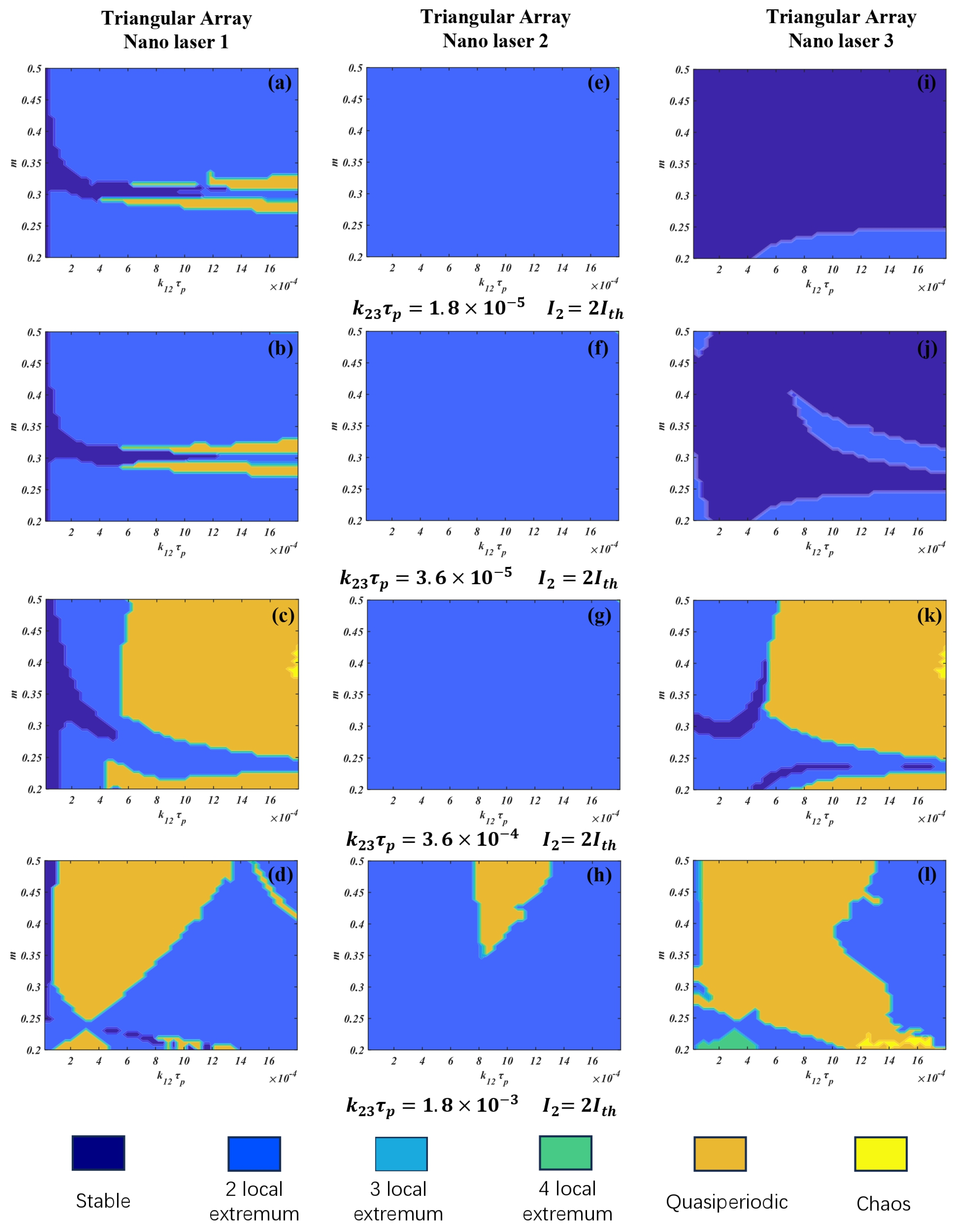
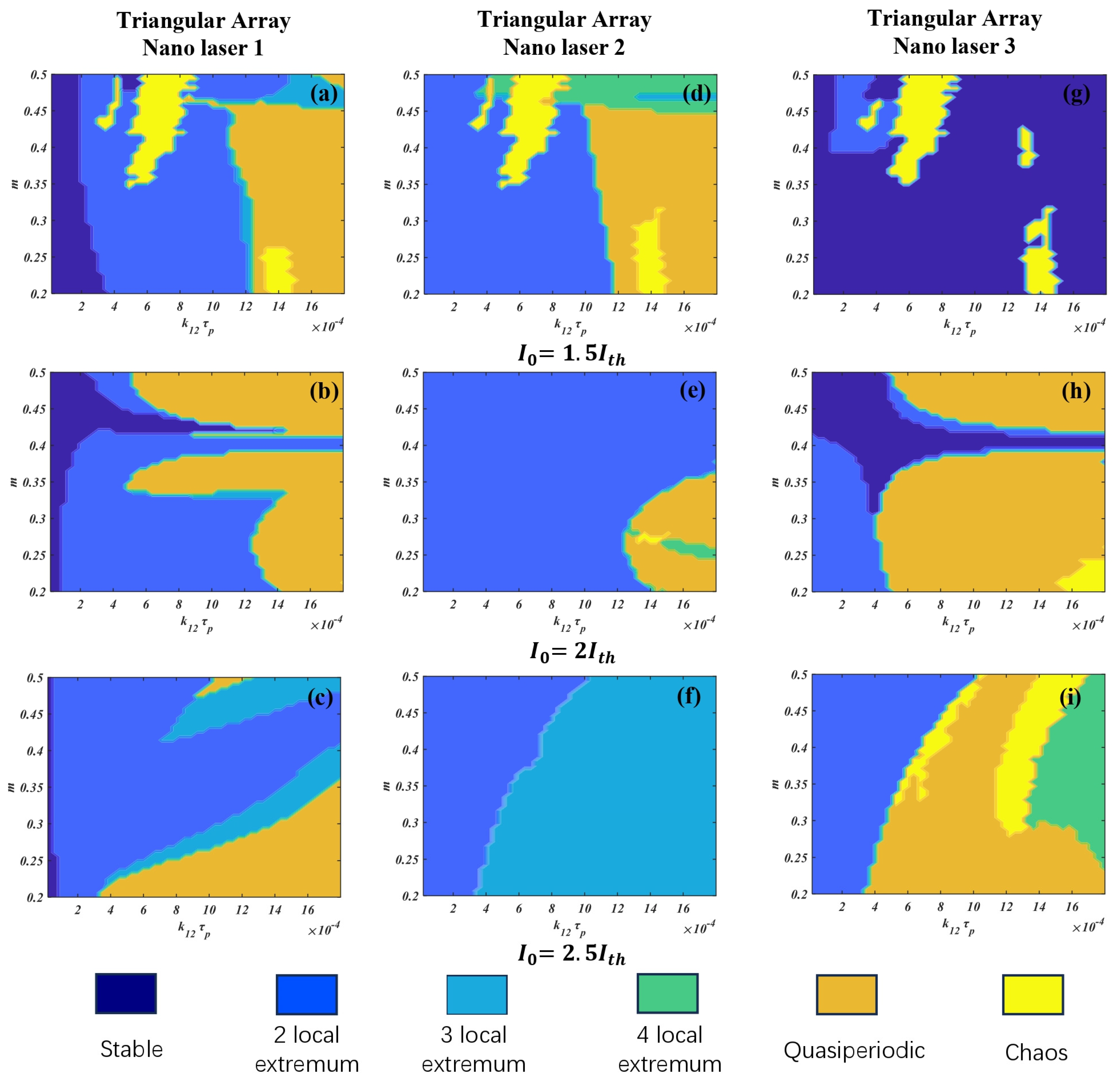
3.2. Triangular Array
4. Conclusions
Author Contributions
Funding
Data Availability Statement
Conflicts of Interest
References
- Ning, C.Z. Semiconductor Nanolasers. Phys. Status Solidi 2010, 247, 774–788. [Google Scholar] [CrossRef]
- Saxena, D.; Mokkapati, S.; Jagadish, C. Semiconductor Nanolasers. IEEE Photonics J. 2012, 4, 582–585. [Google Scholar] [CrossRef]
- Gu, Q.; Fainman, Y. Semiconductor Nanolasers; Cambridge University Press: Cambridge, UK, 2017. [Google Scholar]
- Ma, R.-M.; Oulton, R.F. Applications of Nanolasers. Nat. Nanotechnol. 2019, 14, 12–22. [Google Scholar] [CrossRef] [PubMed]
- Nezhad, M.P.; Simic, A.; Bondarenko, O.; Slutsky, B.; Mizrahi, A.; Feng, L.; Lomakin, V.; Fainman, Y. Room-Temperature Subwavelength Metallo-Dielectric Lasers. Nat. Nanotechnol. 2010, 4, 395–399. [Google Scholar] [CrossRef]
- Hou, Y.; Renwick, P.; Liu, B.; Bai, J.; Wang, T. Room Temperature Plasmonic Lasing in a Continuous Wave Operation Mode from an InGaN/GaN Single Nanorod with a Low Threshold. Sci. Rep. 2014, 4, 5014. [Google Scholar] [CrossRef]
- Li, C.; Wright, J.B.; Liu, S.; Lu, P.; Figiel, J.J.; Leung, B.; Chow, W.W.; Brener, I.; Koleske, D.D.; Luk, T.-S.; et al. Nonpolar InGaN/GaN Core–Shell Single Nanowire Lasers. Nano Lett. 2017, 17, 1049–1055. [Google Scholar] [CrossRef] [PubMed]
- Song, D.I.; Yu, A.; Samutpraphoot, P.; Lee, J.; Kim, M.; Park, B.J.; Sipahigil, A.; Kim, M.-K. Three-Dimensional Programming of Nanolaser Arrays through a Single Optical Microfiber. Optica 2022, 9, 1424. [Google Scholar] [CrossRef]
- Hill, M.T.; Oei, Y.-S.; Smalbrugge, B.; Zhu, Y.; De Vries, T.; Van Veldhoven, P.J.; Van Otten, F.W.M.; Eijkemans, T.J.; Turkiewicz, J.P.; De Waardt, H.; et al. Lasing in Metallic-Coated Nanocavities. Nat. Photonics 2007, 1, 589–594. [Google Scholar] [CrossRef]
- Lee, J.H.; Khajavikhan, M.; Simic, A.; Gu, Q.; Bondarenko, O.; Slutsky, B.; Nezhad, M.P.; Fainman, Y. Electrically Pumped Sub-Wavelength Metallo-Dielectric Pedestal Pillar Lasers. Opt. Express 2011, 19, 21524. [Google Scholar] [CrossRef]
- Ding, K.; Liu, Z.C.; Yin, L.J.; Hill, M.T.; Marell, M.J.H.; Van Veldhoven, P.J.; Nöetzel, R.; Ning, C.Z. Room-Temperature Continuous Wave Lasing in Deep-Subwavelength Metallic Cavities under Electrical Injection. Phys. Rev. B 2012, 85, 041301. [Google Scholar] [CrossRef]
- Ding, K.; Hill, M.T.; Liu, Z.C.; Yin, L.J.; Van Veldhoven, P.J.; Ning, C.Z. Record Performance of Electrical Injection Sub-Wavelength Metallic-Cavity Semiconductor Lasers at Room Temperature. Opt. Express 2013, 21, 4728. [Google Scholar] [CrossRef]
- Li, K.H.; Liu, X.; Wang, Q.; Zhao, S.; Mi, Z. Ultralow-Threshold Electrically Injected AlGaN Nanowire Ultraviolet Lasers on Si Operating at Low Temperature. Nat. Nanotechnol. 2015, 10, 140–144. [Google Scholar] [CrossRef]
- Ren, K.; Li, C.; Fang, Z.; Feng, F. Recent Developments of Electrically Pumped Nanolasers. Laser Photonics Rev. 2023, 17, 2200758. [Google Scholar] [CrossRef]
- Lorke, M.; Suhr, T.; Gregersen, N.; Mørk, J. Theory of Nanolaser Devices: Rate Equation Analysis versus Microscopic Theory. Phys. Rev. B 2013, 87, 205310. [Google Scholar] [CrossRef]
- Romeira, B.; Fiore, A. Purcell Effect in the Stimulated and Spontaneous Emission Rates of Nanoscale Semiconductor Lasers. IEEE J. Quantum Electron. 2018, 54, 1–12. [Google Scholar] [CrossRef]
- Fan, Y.; Hong, Y.; Li, P. Numerical Investigation on Feedback Insensitivity in Semiconductor Nanolasers. IEEE J. Sel. Top. Quantum Electron. 2019, 25. [Google Scholar] [CrossRef]
- Sattar, Z.; Shore, K. Analysis of the Direct Modulation Response of Nanowire Lasers. J. Light. Technol. 2015, 33, 3028–3033. [Google Scholar] [CrossRef]
- Jiang, P.; Zhou, P.; Li, N.; Mu, P.; Li, X. Optically Injected Nanolasers for Time-Delay Signature Suppression and Communications. Opt. Express 2020, 28, 26421. [Google Scholar] [CrossRef] [PubMed]
- Rasmussen, T.S.; Mork, J. Theory of Microscopic Semiconductor Lasers with External Optical Feedback. Opt. Express 2021, 29, 14182. [Google Scholar] [CrossRef] [PubMed]
- Abdul Sattar, Z.; Shore, K.A. Phase Conjugate Feedback Effects in Nano-Lasers. IEEE J. Quantum Electron. 2016, 52. [Google Scholar] [CrossRef]
- Han, H.; Shore, K.A. Dynamics and Stability of Mutually Coupled Nano-Lasers. IEEE J. Quantum Electron. 2016, 52, 1–6. [Google Scholar] [CrossRef]
- Deka, S.S.; Jiang, S.; Pan, S.H.; Fainman, Y. Nanolaser Arrays: Toward Application-Driven Dense Integration. Nanophotonics 2020, 10, 149–169. [Google Scholar] [CrossRef]
- Fan, Y.; Shore, K.A.; Shao, X. Dynamics of electrically-pumped semicondcutor nano-laser arrays. Photonics 2023, 10, 1249. [Google Scholar] [CrossRef]
- Wang, S.S.; Winful, H.G. Dynamics of Phase-Locked Semiconductor Laser Arrays. Appl. Phys. Lett. 1988, 52, 1774–1776. [Google Scholar] [CrossRef]
- Jiang, S.; Deka, S.; Pan, S.H.; Fainman, Y. Effects of High β on Phase-Locking Stability and Tunability in Laterally Coupled Lasers. IEEE J. Sel. Top. Quantum Electron. 2022, 28, 1–12. [Google Scholar] [CrossRef]
- Suhr, T.; Gregersen, N.; Yvind, K.; Mørk, J. Modulation Response of NanoLEDs and Nanolasers Exploiting Purcell Enhanced Spontaneous Emission. Opt. Express 2010, 18, 11230. [Google Scholar] [CrossRef]
- Coldren, L.A.; Corzine, S.W. Diode Lasers and Photonic Integrated Circuits; Wiley: New York, NY, USA, 1995. [Google Scholar]
- Hong, H.; Shore, K.A. Modulated mutually coupled nanolasers. IEEE J. Quantum Electron. 2017, 53, 2000208. [Google Scholar]


| Symbol | Physical Meaning | Value |
|---|---|---|
| β | Spontaneous emission factor | 0.05 |
| Γ | Confinement factor | 0.65 |
| τn | Carrier lifetime | 2.00 × 10⁻⁹ s |
| gn | Differential gain | 1.65 × 10⁻¹² m3/s |
| N0 | Carrier density at transparency | 1.10 × 1024 m−3 |
| τp | Photon lifetime | 0.36 × 10⁻¹² s |
| k | Coupling rate | variable |
| α | Linewidth enhancement factor | variable |
| Δω | Frequency detuning | 0 GHz |
| e | Elementary charge | 1.60 × 10⁻¹⁹ C |
| Va | Volume of the active region | 3.96 × 10⁻¹⁹ m3 |
Disclaimer/Publisher’s Note: The statements, opinions and data contained in all publications are solely those of the individual author(s) and contributor(s) and not of MDPI and/or the editor(s). MDPI and/or the editor(s) disclaim responsibility for any injury to people or property resulting from any ideas, methods, instructions or products referred to in the content. |
© 2023 by the authors. Licensee MDPI, Basel, Switzerland. This article is an open access article distributed under the terms and conditions of the Creative Commons Attribution (CC BY) license (https://creativecommons.org/licenses/by/4.0/).
Share and Cite
Fan, Y.; An, S.; Shore, K.A.; Shao, X. Tailoring the Direct Current Modulation Response of Electrically Pumped Semiconductor Nano-Laser Arrays. Photonics 2023, 10, 1373. https://doi.org/10.3390/photonics10121373
Fan Y, An S, Shore KA, Shao X. Tailoring the Direct Current Modulation Response of Electrically Pumped Semiconductor Nano-Laser Arrays. Photonics. 2023; 10(12):1373. https://doi.org/10.3390/photonics10121373
Chicago/Turabian StyleFan, Yuanlong, Siyi An, K. Alan Shore, and Xiaopeng Shao. 2023. "Tailoring the Direct Current Modulation Response of Electrically Pumped Semiconductor Nano-Laser Arrays" Photonics 10, no. 12: 1373. https://doi.org/10.3390/photonics10121373
APA StyleFan, Y., An, S., Shore, K. A., & Shao, X. (2023). Tailoring the Direct Current Modulation Response of Electrically Pumped Semiconductor Nano-Laser Arrays. Photonics, 10(12), 1373. https://doi.org/10.3390/photonics10121373