1. Introduction
With the development of artificial intelligence technology, various industries are deeply integrating with intelligent information technology. Due to the increasing prominence of issues such as the slowing of Moore’s Law, the “power wall” [
1], and the “von Neumann bottleneck” [
2,
3] in traditional electronic integrated circuits, silicon-based optoelectronic platforms are emerging as promising new technologies in the “post-Moore’s Law” era [
4]. These can greatly reduce the limitations on the development and application of artificial intelligence technology and have become the main direction of widespread attention and breakthroughs in the industry at home and abroad [
5]. In the optical interconnect and optical computing network of the silicon-based photonic platform, a large number of passive devices are employed for controlling the transmission [
6,
7,
8], coupling [
9,
10], and power distribution of light. Among these, optical splitters, as essential components in ultra-compact photonic integrated circuits, play a crucial role in various domains, including sensors, optical switches, logic gates, modulators, signal processing, and more. Additionally, the rapid advancement of MDM technology enables power splitters supporting multiple modes to enhance the transmission and processing speed of high-capacity information greatly. Presently, common multimode power splitters include devices such as multimode interference couplers (MMI) [
11,
12] and directional couplers (DC) [
9,
13]. These couplers have limited-wavelength bandwidth support and require complex designs to achieve arbitrary power splitting ratios (PSRs), which significantly restricts their utility in on-chip MDM applications. Therefore, designing a broadband multimode splitter with arbitrary PSRs remains a challenging and strategically significant endeavor.
In this work, inspired by geometric optical prisms, we propose a novel multimode 2 × 2 power splitter. When light waves pass through the etched subwavelength grating (SWG) in this multimode beam splitter, they undergo frustrated total internal reflection (FTIR), which enables the transmission of some light waves while reflecting others. Moreover, by adjusting the filling coefficient of the SWG material, we can flexibly control the PSR between the reflected and transmitted light waves. We employ 2.5 D Variational Finite-difference time-domain (VARFDTD) simulations and optimization to design the structure of this power splitter, aiming to achieve high-performance broadband power distribution for multimode signals while reducing the device’s dependence on etching processes. On the one hand, to enhance device performance, we have designed slight offsets for our SWG and the output ports for transmission relative to the intersection point of the input and reflector waveguide centers to compensate for the effects of Goos–Hänchen (GH) shift and the transmission offset generated by the SWG layer. On the other hand, to simplify device fabrication, we investigate the impact of grating filling materials and device cladding materials on device performance and grating dimensions. Ultimately, our proposed multimode power splitter achieves power distribution of TE0–TE9-mode light waves at arbitrary ratios within the wavelength range of 1200 nm to 1700 nm. Furthermore, the power splitter exhibits EL of less than 1.1 dB for various mode light waves, and the insertion loss (IL) variation and inter-mode CT for different mode light waves at the same wavelength and output port are both less than 1 dB and −18.8 dB, respectively.
2. Device Design
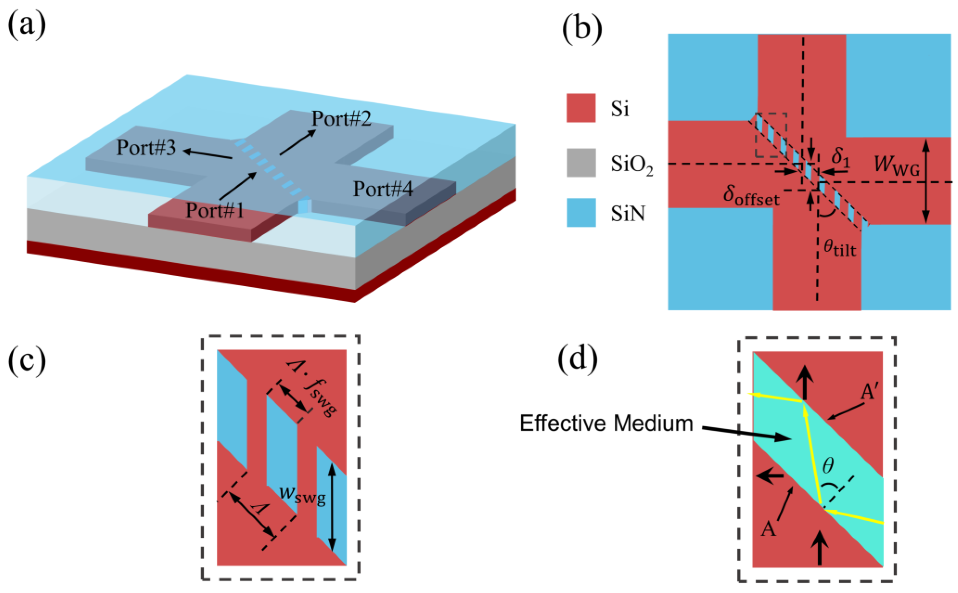
The multimode power splitter is designed on a standard silicon-on-insulator (SOI) substrate with a 220 nm thick top Si layer and a 2 μm thick buried oxide. It is covered by a 2 μm thick Si
3N
4 material, which serves as both the cladding structure and the filling material for the SWG, as shown in
Figure 1a.
Figure 1b shows that the core of the device consists mainly of a cross-shaped Si waveguide with a width of
and a centrally tilted (
= 45°) SWG. The multimode power splitter draws inspiration from the structure of a spectral prism, which gives it characteristics similar to those of a spectral prism. Specifically, the light wave mode incident from input port #1 is divided into two beams by the SWG, exiting from port #2 and port #3, respectively. Likewise, if light enters from port #2, it is divided into two beams, exiting from port #1 and port #4, with the PSR remaining unchanged.
To prevent the shift of light waves caused by transmission and reflection through the SWG layer from affecting the performance of the output ports, there is a longitudinal offset
and a lateral offset
between SWG and port #2 relative to the intersection points of port #1 and port #3 waveguide centers, as illustrated in
Figure 1b. We provide a detailed definition of the SWG period
and the SWG filling coefficient
in
Figure 1c. According to the characteristics of the SWG and the principles of geometric optics, the SWG can be considered equivalent to a single-layer dielectric [see
Figure 1d].
According to the Fresnel formula, the reflectance and transmittance of TE-polarized mode incident waves on a single-layer dielectric layer can be expressed as:
where
is the refractive index of the Si waveguide core layer,
is the refractive index corresponding to the SWG equivalent to a single-layer dielectric,
is the incident angle of the beam,
is the angle of refraction and reflection at interfaces
and
within the equivalent single-layer dielectric, and
is the phase shift within the effective dielectric layer. According to Equations (1) and (2), the PSR of the SWG reflector is obtained as:
The
in Equations (4)–(6) can be obtained using the Rytov [
14] formula:
where
and
represent the ordinary/extraordinary effective medium indices, indicating that SWG is essentially birefringent [
15].
is the refractive index of the filling medium in SWG. The Rytov formula is derived using a zeroth-order approximation, assuming
. For smaller values of
, higher-order approximation expressions of the Rytov formula [
16,
17] can be used to improve accuracy.
As shown in
Figure 1d, due to the half-wave loss generated when light is incident from an optically sparse medium and reflected from an optically dense medium, resulting in additional optical path difference, the phase shift
within the effective dielectric layer can be obtained from the following equation [
18]:
where
is the effective wave vector (
, where
is the wave vector of incident light in vacuum), and
is the width of the SWG [see
Figure 1c]. According to Equation (7),
δ is influenced by
and
, Moreover, Equations (1)–(7) reveal that
,
, and
are all dependent on
associated with
. Consequently, the PSR between the reflected wave and the transmitted wave can be flexibly designed by adjusting
and
of the SWG reflector in Equations (4)–(7).
3. Simulation and Analysis
Due to the excellent compatibility of SiO
2 and Si
3N
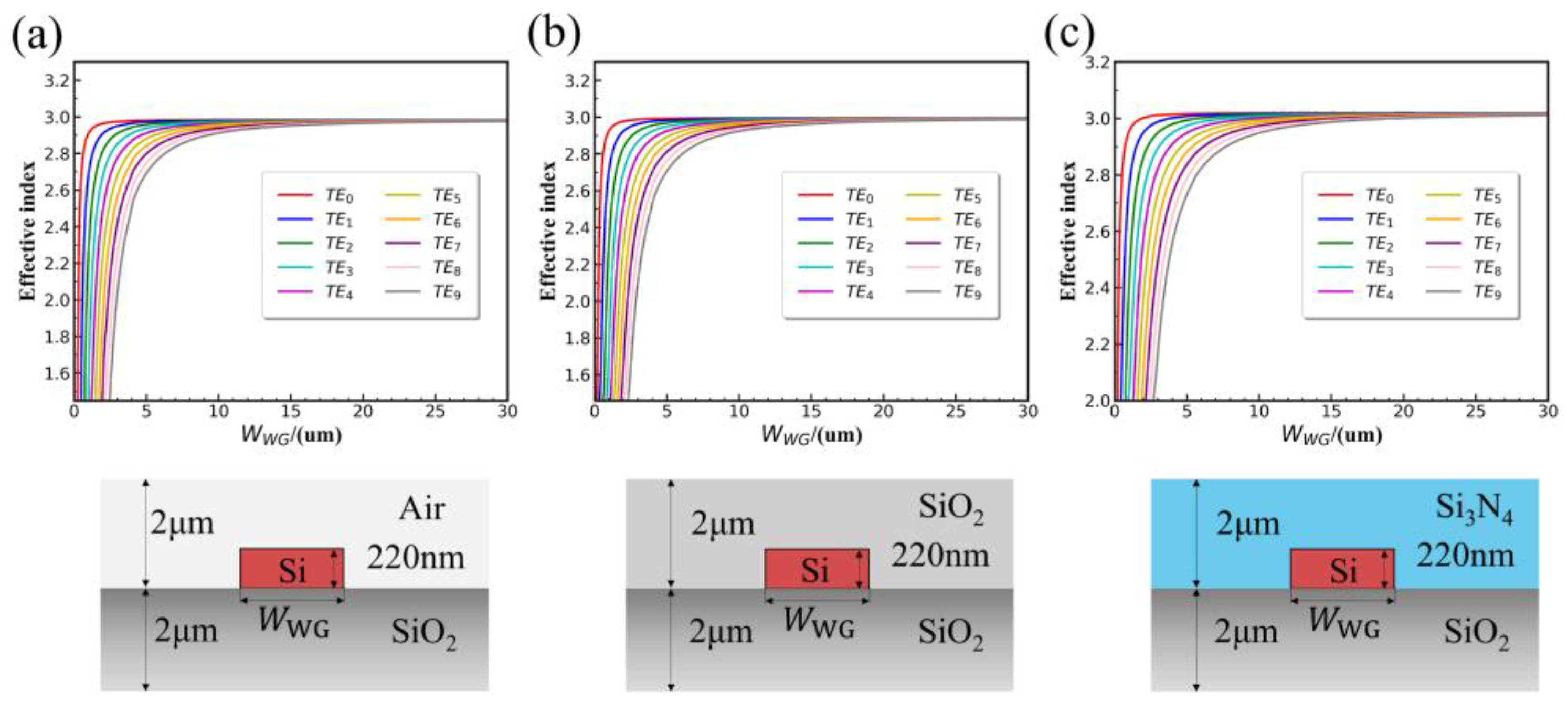
4 with the SOI platform and the mature growth process on Si, they can serve as ideal cladding materials. Furthermore, since other photonic devices in our research project primarily operate around a wavelength of 1310 nm, we used the finite element method (FEM) to simulate the effect of changing the Si waveguide width on the effective refractive index of TE
0–TE
9 mode light in different cladding scenarios at this wavelength. The simulation results in
Figure 2 show that when the cladding structures are Air,
, and Si
3N
4, as the central waveguide width
increases, the effective refractive index of TE
0–TE
9 modes in the waveguide gradually approaches equality. When
> 8 μm, the effective refractive index of low-order modes TE
0–TE
3 becomes closer. Considering that overly large dimensions would dramatically increase the subsequent simulation and modeling time for the device, we chose to investigate the output characteristics of ports #2 and #3 of the power splitter in TE
0–TE
3 modes for these three cladding structures with
= 8 μm.
Based on the diffraction theory of gratings, when the grating period is much smaller than the operating wavelength, only zero-order diffraction will occur. At this point, the SWG can be effectively considered to be a single-layer dielectric, and its effective refractive index is influenced by the SWG filling structure. Therefore, specific PSRs can be achieved by designing the SWG filling structure appropriately. To ensure that the light emitted from port #2 and port #3 undergoes only zero-order diffraction, both the diffraction angles (including reflection and transmission) and the angle of incidence of the grating must be equal. Only specular reflection and direct transmission occur with no backward reflection. Therefore, to suppress backward reflection, the following conditions [
19] should be satisfied:
where
is the effective refractive index of the given mode, and
is the operating wavelength. From Formula (8), it can be observed that as
increases and
decreases, the value of the maximum grating period
decreases accordingly. To meet the requirements of all three cladding structures for suppressing backward reflection, the scenario with the maximum
value is chosen to be used in Equation (8) for calculations. As shown in
Figure 3, when
> 8 μm, the
for TE
0–TE
3 mode waves in devices with the three cladding structures are quite close. Therefore, we study the impact of the three cladding structures on the power splitter performance at this width. Since under the same
conditions, the waveguide’s
using SiO
2 and Air cladding structures is lower compared to Si
3N
4, plugging in the
value for TE
0–TE
3 modes under the Si
3N
4 cladding structure (
= 3.018) into Equation (8) yields a value of
= 0.25 μm. Taking into consideration the suppression of backward reflection for shorter wavelength light waves,
= 0.2 μm is chosen.
Without considering grating transmission offset and GH shift, we employ the VARFDTD method to simulate the effects of varying
and
on the PSR and EL of TE
0–TE
3 modes in devices with three cladding structures when 1310 nm wavelength light waves are incident, as shown in
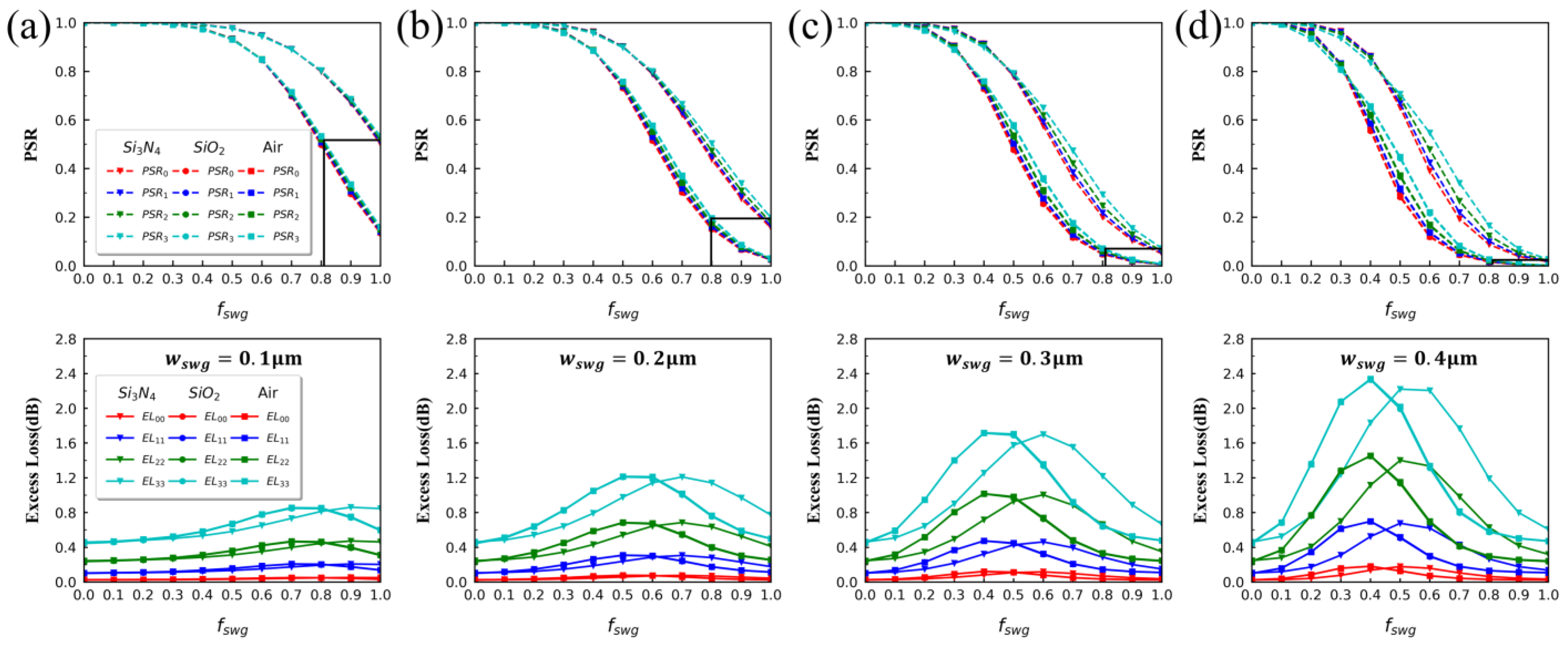
Figure 3a–c. To meet simulation accuracy requirements, the grid resolution at the SWG is set to dx = dy = dz = 10 nm. The formulas for calculating EL and PSR are as follows:
where
is the transmittance of input mode TE
i (
i = 0, 1, 2, 3) generating mode TE
j (
j = 0, 1, 2, 3) at ports
k (
k = 2, 3).
here denotes the PSR when the corresponding emission mode is TE
i. It can be observed that the
varies with changes in
,
, and
. However, for
i = 0, 1, 2, 3, the
changes are nearly identical due to the similarity in effective refractive indices of these modes, as shown in
Figure 3a.
The simulation and calculations in
Figure 3 reveal that only at
≥ 0.3 μm, there is a significant difference in the PSR of TE
3 mode compared to other lower-order modes. This is due to the significant difference in the
of TE
3 mode compared to other lower-order modes in the simulated Si waveguide structure, and this effect can be reduced by increasing
. Furthermore, from
Figure 3, it is evident that in multimode power splitters with Air and SiO
2 cladding structures, the EL and PSR curves for TE
i (
i = 0, 1, 2, 3) almost coincide. In contrast, for multimode power splitters with Si
3N
4 cladding structures, there is a noticeable deviation in the EL and PSR curves compared to the other two cladding structures. This difference is reflected in two aspects: first, when Si
3N
4 is used as the cladding structure, the PSR exhibits a smoother transition above the horizontally marked line in
Figure 3a–d compared to the other two cladding structures. It is less sensitive to changes in
and thus achieves superior etching tolerance for the device. Second, when the three cladding structures achieve the same PSR in the power splitter, as shown in
Figure 3a–d EL curves, it can be seen that the EL of
in the power splitter with Si
3N
4 cladding is smaller than in the other two cladding structures, indicating lower loss. The reason for the aforementioned differences is that, in these two structures, the effective refractive index curves of mode
in the Si waveguide are nearly identical, and both differ significantly from the effective refractive index curve in the Si
3N
4 structure, as can be seen in
Figure 2a,b.
The above results and analysis indicate that using Si3N4 as the cladding structure for multimode power splitters performs better in etching processes and device performance compared to the other two cladding structures. To achieve a wide range of PSR, low EL, and lower mode sensitivity, we ultimately selected as 0.2 μm and 0.3 μm for the subsequent simulation.
On the one hand, due to the presence of GH shift, the actual reflection interface experiences displacement relative to interface A [see
Figure 1d], resulting in a mode–field mismatch between the output mode and port #3 (reflection port). It is necessary to eliminate this mode–field mismatch to avoid additional losses and PSR errors. For TE-polarized modes, the required mirror offset
to compensate for GH offset can be derived as [
8]:
where
is the wave vector of incident light in a vacuum, with a value of
.
represent the effective refractive indices of the corresponding mode in the SWG layer, respectively. By combining Equation (4), it becomes evident that in multimode simulation scenarios, the value
is influenced by
.
On the other hand, as light is input from port #1 and undergoes reflection and refraction within the SWG before being output from port #2, the presence of SWG leads to an optical wave experiencing a transmission offset as it passes through the equivalent dielectric layer. This transmission offset distance can be calculated using the steady-state phase theory [
20,
21]:
where
A and
B represent coefficients associated with
,
,
, and
. it can be seen that
, relative to
, is influenced not only by
but also affected by
.
From
Figure 3b, it can be observed that when
= 0.2 μm and
= 0.8, or
= 0.3 μm and
= 0.65, the PSR of the four modes is around 0.5, indicating even power splitting at both output ports. We can more easily observe the impact of grating transmission offset and GH displacement on the two output ports in this situation. Using Snell’s law
= and Equations (4)–(6), we can calculate the value of
by substituting
,
, and
, and then determine the value of
. With the value of
and the SWG cladding structure, we can use FEM to calculate that
is 2.04 and 2.18 under the two conditions. Plugging these values into Equations (11) and (12) yields
and
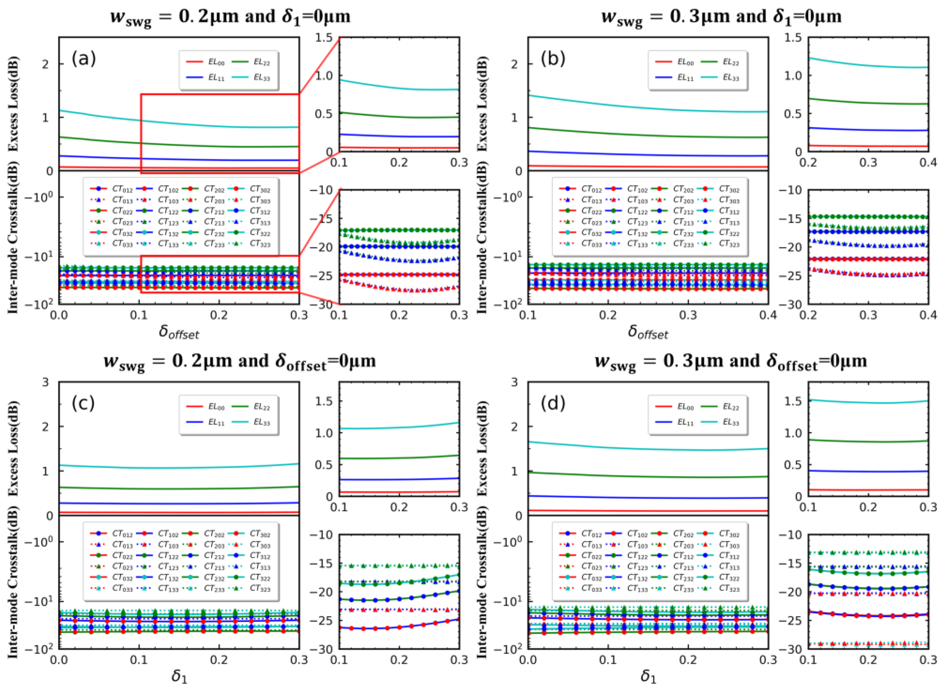
values of 0.23 μm, 0.17 μm, and 0.32, 0.25 μm, respectively. To validate the accuracy of this calculation, we conducted simulations using the VARFDTD method to assess the impact of
and
displacements on the ELs and inter-mode CTs of
modes at output ports #2 and #3 in the entire device, with the grid resolution at SWG set to dx = dy = dz = 10 nm, and the simulation results are shown in
Figure 4. CT is derived from the following equation:
Where
represents the crosstalk of mode TE
j (
j = 0, 1, 2, 3) relative to mode TE
i (
i = 0, 1, 2, 3) at ports
k (
k = 2, 3). From
Figure 4a,b, it can be observed that when
is 0.23 μm and 0.32 μm, the CT effects on the four modes are weakest, and the values of ELs are minimized. The increase in
has a much larger impact on the CTs of modes output from port #3 compared to those output from port #2. From
Figure 4c,d, it can be seen that when
is 0.16 μm and 0.24 μm, the ELs for the two modes are minimal. Additionally, unlike the impact of
on port #3, the variation of
has a more significant effect on the CTs of modes at port #2. Considering the simulation step size, these simulation results are consistent with the GH shift behavior predicted by Equation (11) and the transmission shift behavior predicted by Equation (12). Furthermore, from
Figure 4a–d, it can be observed that when
and
deviations relative to the target values are within 20 nm, and the changes in EL and CTs are less than 0.02 dB and 0.5 dB, respectively, indicating good manufacturing robustness of the device. When
> 8 μm, it can be observed from
Figure 2c that changing the
has a very small impact on
, and similarly, the value of
remains nearly unchanged. Therefore, at
= 30 μm, the values of
and
influenced by this factor also do not change significantly. To compensate for the GH shift and transmission shift,
and
can be selected as 0.23 μm and 0.17 μm, respectively, at
= 0.2 μm, or 0.32μm and 0.25μm, respectively, at
= 0.3 μm to achieve optimal device performance.
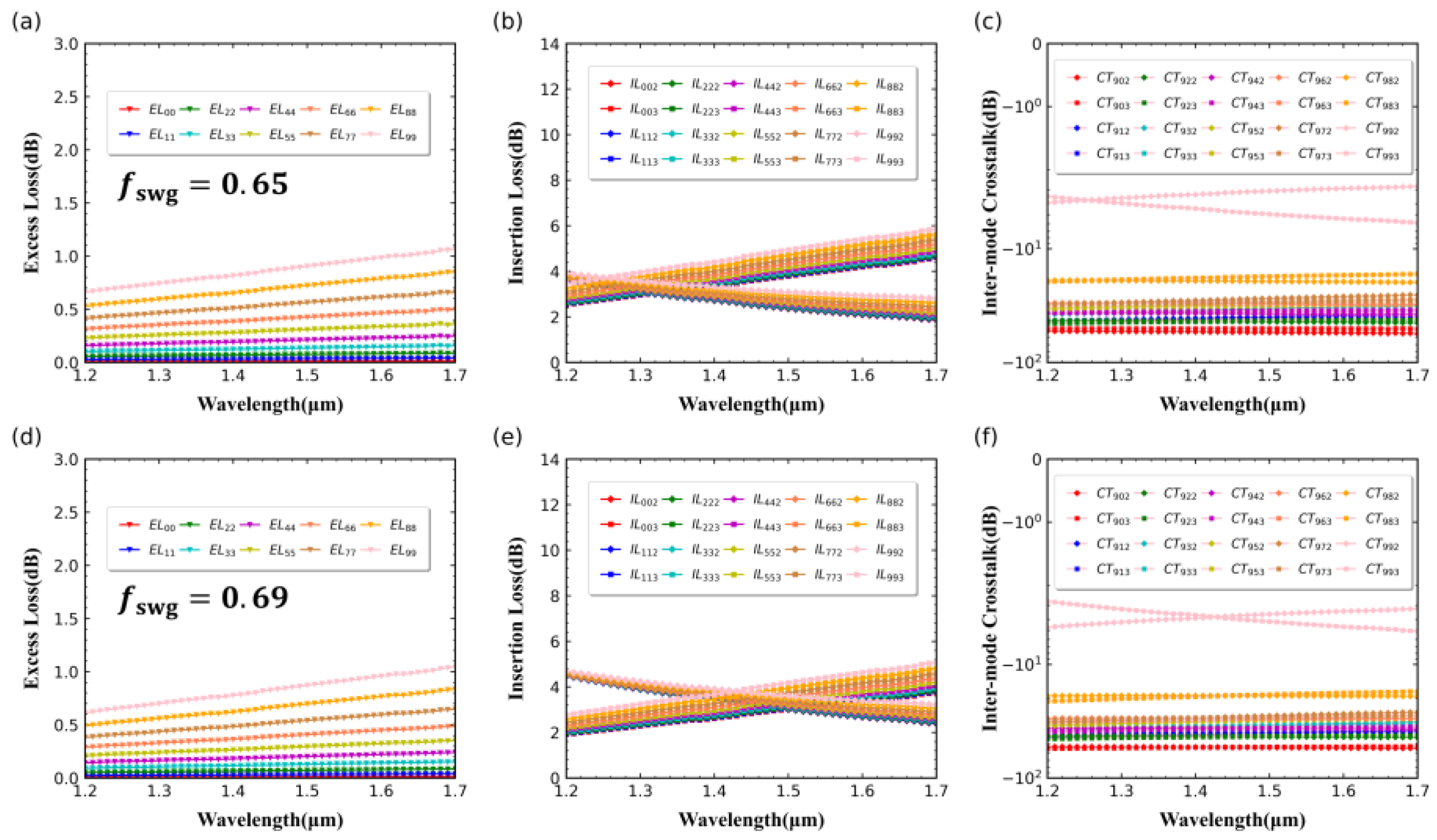
To visually demonstrate the multimode scalability of the power splitter, we used the VARFDTD method to simulate the ILs, ELs for each mode, and inter-mode CTs for TE
0–TE
9 modes in the multimode power splitter at
= 30 μm,
= 0.3 μm, and
values of 0.65 and 0.69 over a wavelength range of 1200–1700 nm at output ports #2 and #3 relative to the input port. The results are shown in
Figure 5. The IL can be determined using the following formula:
where
represents the insertion loss of mode TE
j (
j = 0, 1, 2, 3) relative to mode TE
i (
i = 0, 1, 2, 3) at ports
k (
k = 2, 3).
As shown in
Figure 3c earlier, at
= 0.65, the multimode power splitter achieves uniform power splitting for TE
0–TE
3 optical waves at 1310 nm wavelength with
= 8 μm. In
Figure 5a–c, it can be observed that at
= 30 μm, the device achieves uniform power splitting for TE
0–TE
5 and even higher-order modes at 1310 nm wavelength, demonstrating excellent multimode expansion performance.
Figure 5d–f reveals that at
= 0.69, the device achieves relatively uniform power splitting for TE
0–TE
5 at 1450 nm wavelength, with ELs for TE
0–TE
5 modes below 0.5 dB across the simulated wavelength range of 1200–1700 nm, and their IL curves largely overlap. however, ELs for TE
6–TE
9 modes increase significantly.
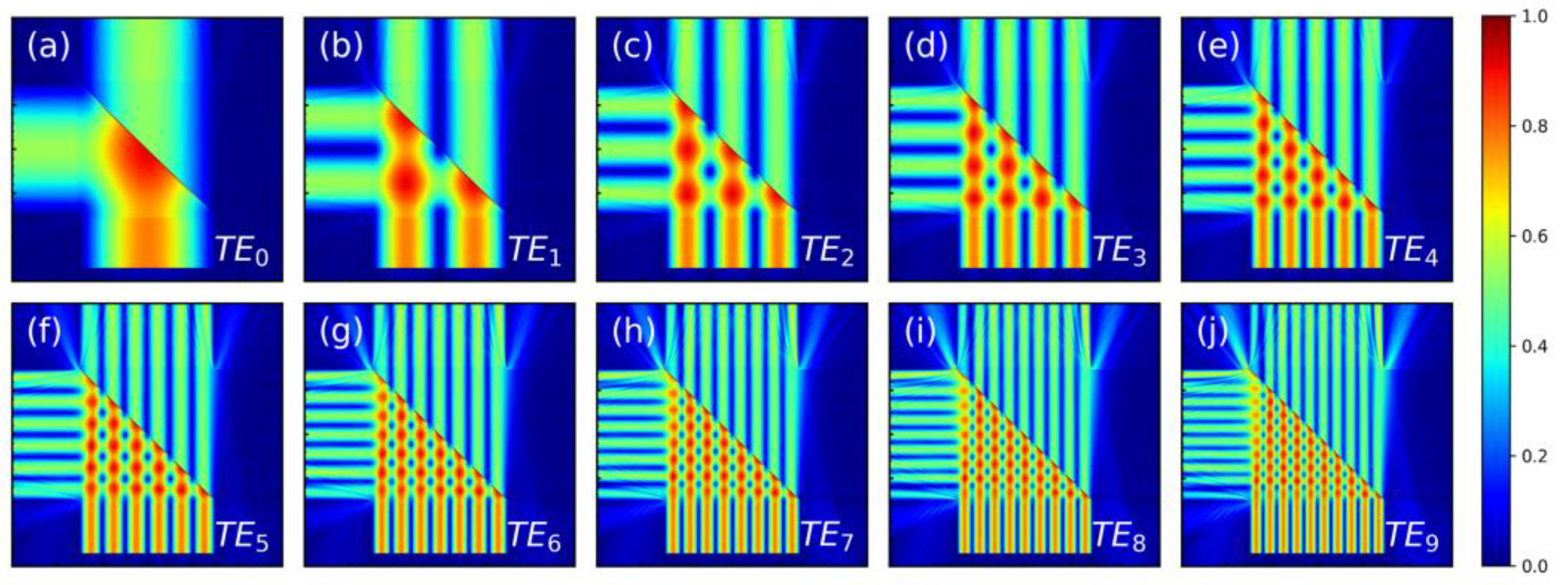
Figure 6g–j illustrates the electric field distribution of TE
6–TE
9 modes at 1450 nm wavelength and
= 0.69, showing that TE
6–TE
9 modes leak noticeably into the cladding due to reduced confinement at the SWG grating in the Si waveguide. This leakage can be improved by reducing the
difference of higher-order modes. By increasing the
width, it is easy to expand the device to more modes, which can significantly reduce the losses and differences mentioned above.
