1. Introduction
Over the past decade, the development of optical communication technology has led to a substantial increase in global data traffic. Enhancing the speed and capacity of optical communication has become an urgent challenge to address [
1]. Dense wavelength division multiplexing (DWDM) systems have emerged as the preferred solution for various domains, including ultra-large-scale data centers and optical interconnect networks for 5G and 6G communications [
2]. As a critical component within DWDM systems, arrayed waveguide grating (AWG) based on planar waveguide circuits offers advantages such as technological maturity, excellent performance, ease of integration, and relatively low costs [
3]. Therefore, research on AWG in the field of optical communication has received continuous attention and advancement from researchers [
4].
AWG has clear advantages compared to other forms of wavelength division multiplexers such as Mach–Zehnder interferometers [
5], long-period gratings [
6], and Bragg gratings [
7]. Depending on the requirements, AWG can accommodate a sufficient number of output channels with narrow channel spacing while maintaining compactness. Furthermore, the optical performance of AWG exhibits desirable characteristics, including low loss, low crosstalk, high bandwidth, and high spectral resolution. As a result, AWG plays a crucial role in various other research fields, such as astronomy [
8], optical imaging [
9,
10], spectroscopy [
11,
12], optical sensing [
13,
14], biomedical applications [
15], and neural networks [
16,
17]. Moreover, the rapid advancement of AWG technology has led to the diversification of material platforms used for its fabrication, including silicon [
18,
19], silica [
20,
21], SiN [
22,
23,
24], InP [
25], LNOI [
3,
26], and polymers [
15,
27]. Additionally, the application of AWG is not limited to individual devices anymore, as it can be integrated on-chip with other components, such as optical frequency combs [
28], micro-ring resonators [
29,
30], and others. This allows AWG to achieve more versatile functionalities and further expand its two-dimensional and even three-dimensional integration approaches [
28,
31].
The development of AWG with an increased number of output channels and reduced channel spacing is currently a prevailing trend [
4,
19,
21,
32]. However, the addition of more channels and the narrowing of channel spacing present difficulties in ensuring the optical performance of AWG and lead to an increase in their physical size. The center frequency accuracy (CFA) of AWG output channels measures the deviation between the center frequency of each channel and its ideal value. Nevertheless, the greater number of channels and narrower channel spacing pose significant challenges in the design and optimization of CFA [
13,
20,
29,
33]. Factors affecting CFA include not only manufacturing errors and operating temperatures of the devices [
10,
34], but also the improper selection of channel spacing parameters during the design phase of AWG [
35]. In the field of optical communications, particularly in DWDM systems, achieving a high level of CFA is a critical factor in ensuring communication quality. Therefore, it is of utmost importance to identify appropriate optimization methods.
The structure of this paper is organized as follows: In
Section 2, an analysis of the causes of deviations in the center frequency based on the design theory of AWG is presented. In
Section 3, the design of an AWG with 80 output channels using the silica material platform is described.
Section 4 introduces the optimization methods that significantly improve the CFA performance of the designed AWG through a series of optimization steps.
Section 5 and
Section 6 provide an analysis and discussion of the results of the design and optimization work, and is followed by the conclusion.
2. Causalities of Center Frequency Deviation
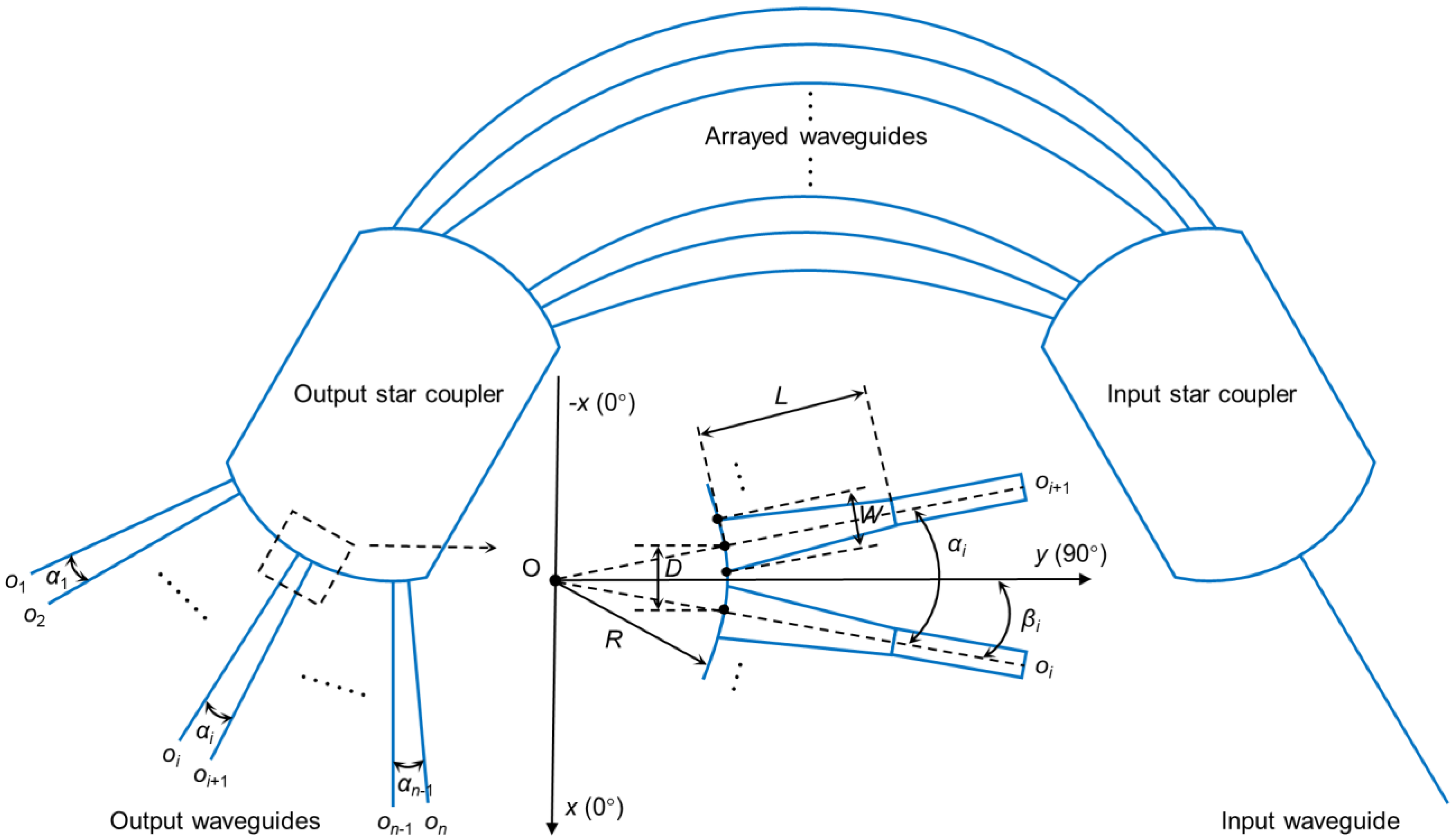
This section focuses on analyzing the reasons for the deviation of the central frequency and provides optimization ideas to improve the CFA. The structure of a typical AWG is shown in
Figure 1, which consists of five main parts: input/output waveguides, input/output star couplers (free propagation region), and an arrayed waveguide section. The working principle of the AWG as a demultiplexer is as follows: Signals consisting of multiple wavelengths enter the device through the input waveguide and undergo diffraction in the input star coupler region. Then, they couple the same phase into the arrayed waveguide section. Due to the constant length difference between adjacent waveguides in the array, signals of the same wavelength have the same phase difference when they reach the output star coupler, while signals of different wavelengths have different phase differences. In the output star coupler region, signals of different wavelengths undergo diffraction and focus on their corresponding output waveguide positions. Finally, the signals are output through the output waveguides, completing the demultiplexing function. If the signals are input in reverse, the above process is reversible, thus achieving the multiplexing function.
Figure 1 illustrates some key structures and parameters involved in the design and optimization process of the AWG. The input waveguide is located in the bottom right corner, while the input/output star couplers are symmetrically distributed on the left and right sides, with the arrayed waveguides positioned in the middle, connecting the two star couplers. The output waveguides are labeled as
o1−
on, and the angular spacing between them is denoted as
α1−
αn-1. Point O represents the center of the Rowland circle, and an (
x,
y) Cartesian coordinate system is established with point O as the origin.
βi represents the angular position of the output waveguide relative to the
y-axis, with values closer to the
y-axis indicating proximity to 90 degrees. On the Rowland circle,
D represents the spacing between output waveguides,
W represents the width of the output waveguide taper,
L represents the length of the output waveguide taper, and
R represents the radius of the Rowland circle. Similarly, the geometric parameters defining the arrayed waveguides on the grating circle are analogous to those of the output waveguides on the Rowland circle. Specifically,
d represents the spacing between arrayed waveguides,
w represents the width of the arrayed waveguide taper,
l represents the length of the output waveguide taper, and
r represents the radius of the grating circle. However, to keep the figure more concise, these parameters are not explicitly labeled in the diagram.
According to the specifications set by the International Telecommunication Union (ITU) regarding the output channel grid for optical communication applications, the output channel spacing of an AWG should adhere to a constant frequency interval rather than a constant wavelength interval. However, the current mainstream commercial AWG design software (such as Rsoft AWG Utility version 2020.03, Optiwave WDM Phasar version 2.0, etc.) commonly utilizes a constant wavelength interval as a fundamental parameter in the design process. As a result, the AWG designed using these software tools often fails to meet the requirement of a constant frequency interval, which is essential for optical communication applications.
According to the relationship between wavelength, speed of light, and frequency, the relationship between wavelength spacing and frequency spacing can be derived as shown in Equation (1).
where Δ
λi denotes the wavelength spacing between the
i-th and (
i + 1)-th output channels, and Δ
fi represents the frequency spacing between the
i-th and (
i + 1)-th output channels. The parameter
c represents the speed of light, while
fi and
fi+1 correspond to the center frequencies of the
i-th and (
i + 1)-th output channels, respectively.
Taking the output waveguides
o1 and
o2 in
Figure 1 as an example, the relationship between their corresponding center wavelengths can be described as
λ1 <
λ2. According to Equation (1), it follows that the relationship between their center frequencies is
f1 >
f2. Therefore, we have Δ
λ1 =
λ2 −
λ1 and Δ
f1 =
f1 −
f2, where Δ
λ1 and Δ
f1 represent the wavelength spacing and frequency spacing, respectively, between the output channels corresponding to waveguides
o1 and
o2. In optical communication applications, the design of AWG often involves selecting a frequency spacing Δ
f for the output channels, such as 50 GHz, 100 GHz, or 200 GHz. According to Equation (1), with the speed of light
c and Δ
fi being constants, as
o1 gradually changes to
on, the values of
fi and
fi+1 decrease, resulting in an increase in Δ
λi. This implies that the wavelength spacing Δ
λi of the output channels in an AWG is not constant; it varies with the numbering of the output waveguides.
The relationship between
αi and the corresponding Δ
λi can be derived from the angular dispersion equation of the AWG output channels, as shown in Equation (2).
where
αi represents the angular spacing between output waveguides; Δ
λi denotes the wavelength spacing between output channels;
m represents the diffraction order;
d stands for the arrayed waveguide spacing;
ng represents the group refractive index of the arrayed waveguide;
ns denotes the effective refractive index of the slab waveguide; and
nc represents the effective refractive index of the rectangular waveguide.
The calculation and determination of αi play a crucial role in the performance of CFA. According to Equations (1) and (2), when all other parameters are constant, a constant Δfi will result in a gradual increase in αi with the increase of Δλi. However, in practical applications, commercial AWG design software often fixes the value of Δλi, which in turn makes αi a constant. This approach overlooks the accuracy of the device’s actual physical structure, leading to deviations in the center frequency of the output channels.
It is noteworthy that the aforementioned center frequency deviations exhibit cumulative behavior. According to Equations (1) and (2), it can be observed that as the number of output channels increases, the accumulated center frequency deviations become more significant for the channels located closer to the edges. This poses a critical optimization challenge for AWG with a high number of channels, particularly in the context of their application in DWDM systems within the field of optical communication.
Apart from adjusting
αi, the constraint relationship and geometric position of the AWG output waveguides also require careful consideration of the values of
βi. As illustrated in
Figure 1,
αi determines the angular spacing between the output waveguides, while
βi determines their angular position relative to the
y-axis. This implies that solely adjusting
αi is insufficient to meet the performance requirements of CFA; appropriate modifications to
βi are also necessary.
Based on the analysis and discussion above, it can be concluded that adjusting and modifying αi and βi are crucial steps in enhancing CFA performance. The specific adjustment methods and details need to be determined based on the designed AWG. The subsequent section will provide a comprehensive discussion on the optimization method for CFA, taking into account the device design considerations.
3. Device Design
In this section, we present an AWG designed for application in DWDM systems. The design of the AWG was carried out using the finite difference beam propagation method (FD-BPM). The AWG has 80 output channels (n = 80), an operating center wavelength (λ0) of 609.95 nm, and an output channel frequency spacing (Δf) of 200 GHz. The core material used is Ge-doped SiO2, and the cladding material is SiO2. The refractive index difference (δ) between the core and cladding materials is 1.5%.
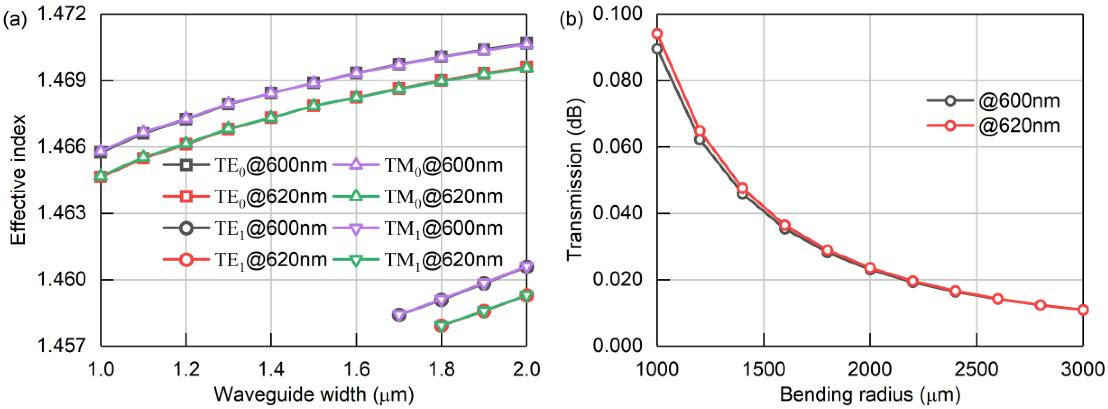
The waveguide type selected for this study is rectangular waveguide, and the determination of the waveguide’s single-mode transmission condition and minimum bending radius was based on simulation results, as shown in
Figure 2. Within a specific wavelength range, when the height of the waveguide is fixed, the number of modes that can be stably transmitted inside the waveguide is determined by the width of the waveguide. Considering the device’s operating center wavelength and AWG design experience, a Ge-doped SiO
2 with a film thickness of 1.5 μm, corresponding to a waveguide height of 1.5 μm, was initially chosen. Subsequently, within the device’s operating wavelength range of 600 nm to 620 nm, the effective refractive index of the TE mode inside the waveguide was simulated at different widths, as depicted in
Figure 2a. It can be observed that with increasing width, higher-order modes gradually appear. The effective refractive index of the TE mode varies for different wavelengths, but the number of supported modes remains relatively consistent for the same width. The simulation results indicate that, under the same parameter settings, the effective refractive index of the TM mode is essentially the same as that of the TE mode. Hence, a waveguide width of 1.5 μm is a suitable choice as it enables single-mode transmission within the designed operating wavelength range. Additionally, in order to achieve a more compact design for the AWG, the bending radius was simulated in
Figure 2b. Here, a segment of waveguide with a height and width of 1.5 μm underwent a 90-degree bend. As the bending radius decreases, the dimensions of the AWG structure can be reduced; however, the loss in the bent section of the waveguide also increases. There is a trade-off between the size and performance of the device. When the bending radius is 2000 μm, the transmittance of the aforementioned 90-degree bent waveguide reaches 99.5%, with a low loss of 0.02 dB. Therefore, the final choice for the minimum bending radius of the waveguide is 2000 μm.
In order to improve the optical performance of the designed AWG, the main structural parameters in
Figure 1 were selected based on the simulation results. The output waveguide spacing, denoted as
D, is a crucial parameter affecting the crosstalk between adjacent output channels (AX).
D needs to be sufficiently large to ensure minimal AX. The array waveguide spacing, denoted as
d, has a significant impact on the insertion loss (IL), with smaller
d values leading to better IL performance. However, smaller
d values may negatively affect insertion loss uniformity (ILU). Increasing the width of the output and array waveguides taper promotes higher coupling efficiency. It is desirable to have
W and
w values as close as possible to
D and
d, respectively. Additionally, a minimum gap of 1.2 μm between the waveguide structures should be maintained to ensure manufacturing feasibility. Since subsequent optimization of CFA requires adjustments to
αi, which may alter the determined value of
D, the difference between
D and
W should be greater than 1.2 μm. The lengths of the output waveguide and array waveguide tapers, denoted as
L and
l, respectively, should not be too small, and their values should be selected based on the corresponding widths to ensure mode decoupling. The ILU is sensitive to the ratio of the Roland circle radius to the grating circle radius. A larger
R/
r ratio straightens the arc of the Roland circle, facilitating better acceptance of diffracted light by the edge output channels. The value of the free spectral range (FSR) is generally 1.5−2 times the number of output channels or even larger, effectively avoiding excessive insertion loss in the edge output channels. The main parameter values of the designed AWG in this study are presented in
Table 1.
Due to the large number of output channels in the designed AWG, improving the ILU performance has become a challenge. Even with the optimization of the aforementioned structural parameters, including
R/
r and FSR, the simulation results indicate that the desired ILU performance target (<0.5 dB) cannot be achieved. Fine adjustments to the width of the output waveguide tapers can effectively address this issue. Typically, output channels in the middle region of the AWG spectrum exhibit lower insertion losses, while those in the edge region experience higher insertion losses. By reducing the width of the output waveguide tapers in the middle region of the spectrum, the insertion losses of the corresponding output channels can be increased, thereby improving the uniformity among all output channels. Following this approach, the width of each output waveguide taper was individually adjusted, as indicated by
W in
Table 1. This followed the principle of larger widths on the sides and smaller widths in the middle, with a nearly linear variation. The width of tapers for output waveguides
o1−
o40 and
o80−
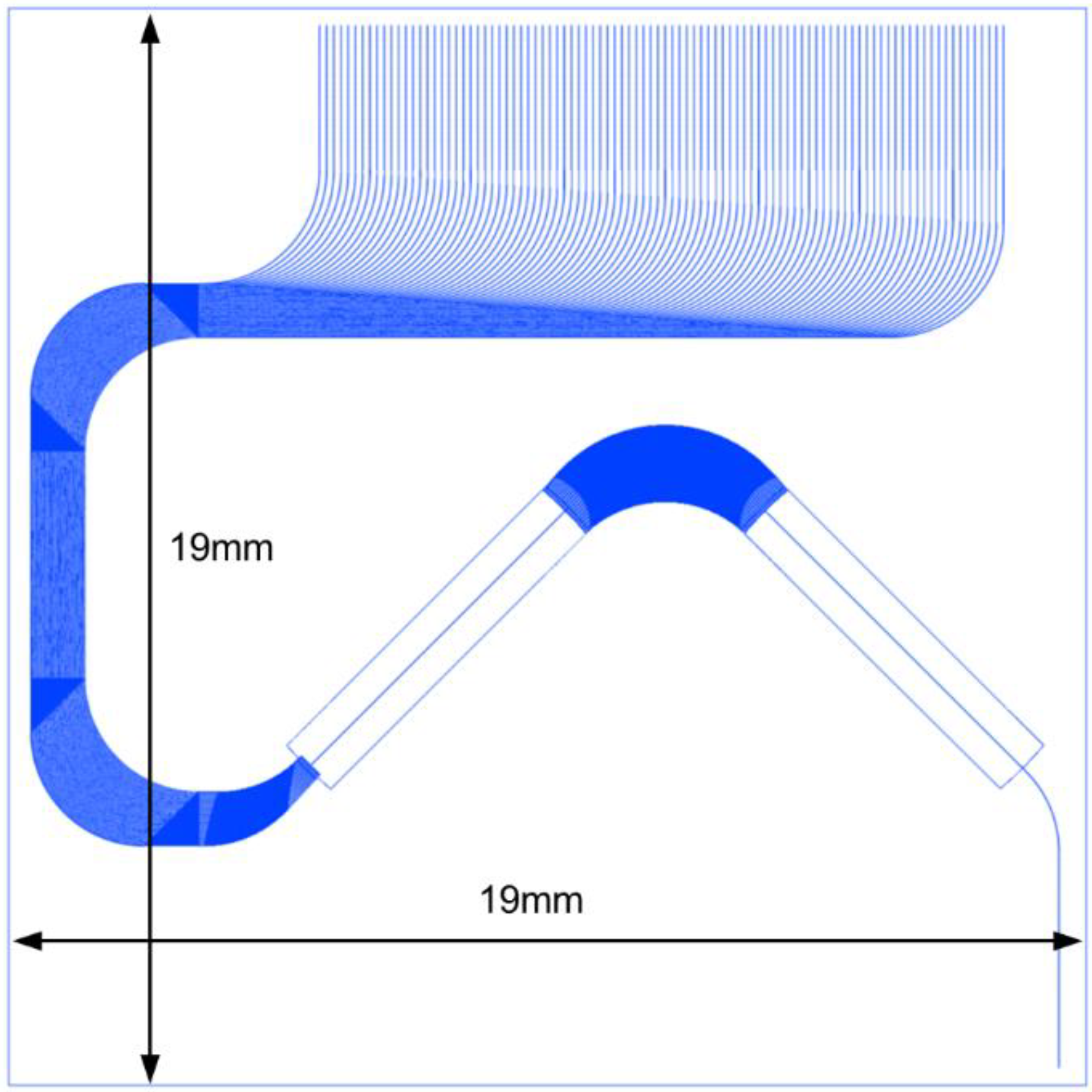
o41 decreased linearly from 3 μm to 1.92 μm, respectively. The simulation results demonstrate that this approach achieves the desired ILU performance target. The final footprint of the designed AWG is 19 × 19 mm², as shown in
Figure 3, and its main optical performance is summarized in
Table 2.
4. Optimization Method of the CFA
In this subsection, we further refine the structural parameters of the designed AWG and propose an optimization method for CFA. By adjusting αi and βi, we make modifications to the constraint relationship and geometric position of the output waveguides. This enables us to achieve a high level of CFA.
According to
Table 2, the CFA without optimization is 67.63 GHz. The CFA values for each output channel are shown in
Figure 4, where the CFA is calculated by subtracting the center frequency of each output channel in the design parameters from the corresponding center frequency in the simulation results.
Figure 4 reveals that the output channels closer to the edges exhibit larger center frequency deviations, while the ones closer to the center show smaller deviations. The center frequency deviations demonstrate a clear cumulative characteristic. Generally, for AWG used in the field of optical communication, the output channel CFA should not exceed 10% of the output channel frequency spacing. The designed AWG in this study has an output channel frequency spacing of Δ
f = 200 GHz, indicating that the CFA should be less than 20 GHz. However, the CFA shown in
Figure 4 significantly exceeds this performance requirement, indicating the need for further improvement.
Based on the previous analysis and discussion, the first adjustment is made to the angular spacing of the output waveguides to correct the constraint relationship of the output waveguides. In the simulation, the channel wavelength spacing Δ
λi is set to 0.25 nm, and the values of
ng,
ns, and
nc are 1.4815, 1.4741, and 1.4687, respectively. The values of
m and
d are referenced in
Table 1. By substituting all the parameters into Equation (2), the value of
αi can be calculated as 0.0441 degrees, and this value is defined as
αi1. A comparison reveals that the value of
αi1 is the same as the initial set value for the output waveguide angular spacing in the simulation.
In order to obtain the correct
αi, it is necessary to first calculate the wavelength spacing Δ
λi that varies with the output channel frequency according to Equation (1) and then substitute it into Equation (2). From
Table 1, it is known that the designed AWG output channel frequency spacing is Δ
f = 200 GHz. The center frequencies of the first and last output channels are
f1 = 499.4 THz and
f80 = 483.6 THz, respectively. Furthermore, the parameters
ng,
ns, and
nc in Equation (2) are wavelength-dependent parameters that vary with wavelength. In particular, the dispersion effect dominates in the arrayed waveguide region of the AWG. Therefore, all parameters related to frequency and wavelength need to be adjusted, including Δ
λi (
f),
ng (
λ),
ns (
λ), and
nc (
λ).
By substituting the adjusted parameters into Equations (1) and (2), the correct output waveguide angular spacing can be calculated and defined as
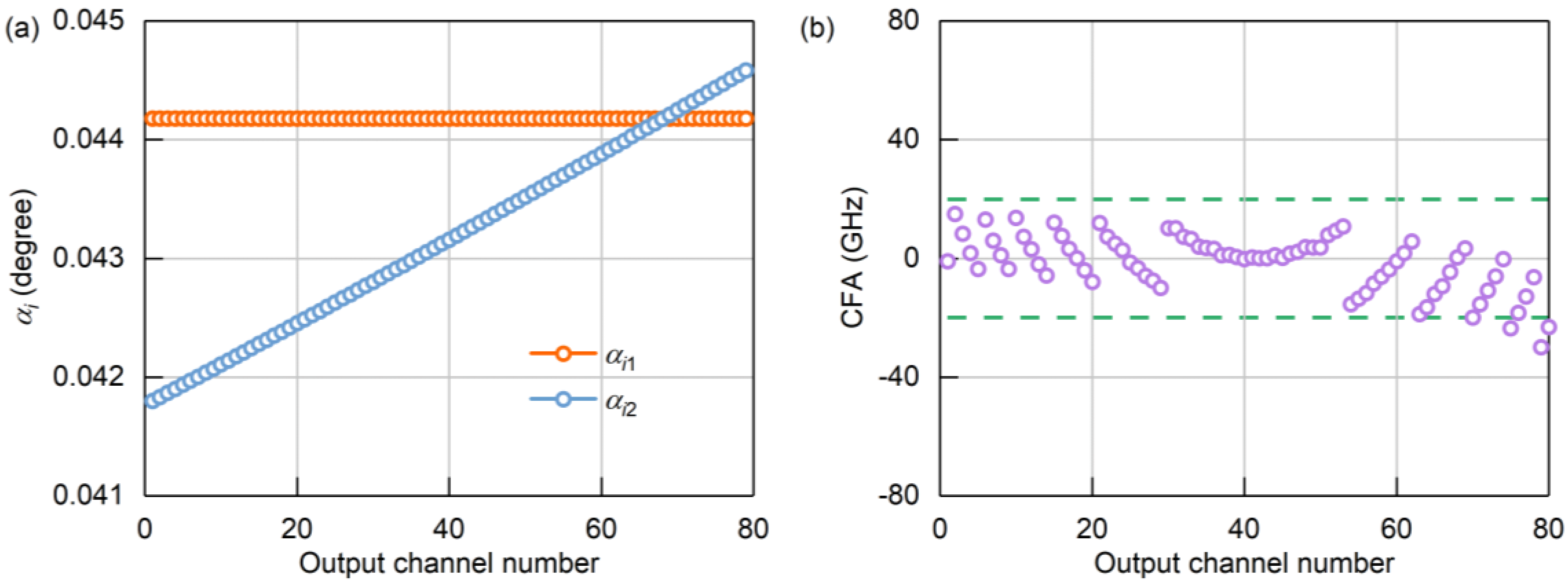
αi2. The comparison of the values between
αi1 and
αi2 is shown in
Figure 5a, where
αi1 is a fixed value, while
αi2 gradually increases with the variation of output channels. This indicates that the arrangement of output waveguides on the Roland circle of the output star coupler is not uniform. Simulating the designed AWG with the adjusted output waveguide angular spacing
αi2, the obtained CFA is shown in
Figure 5b. At this stage, the CFA value is 29.89 GHz, which is very close to the expected optimization target.
Next, the adjustment of the angular position of the output waveguides relative to the
y-axis is carried out. Since the angle adjustment is small, a new variable Δ
βi is defined to represent the change in geometric position. The calculation of Δ
βi is obtained by subtracting the value of
βi before the angular position change from its value after the change. The angular position before adjusting
αi is denoted as
βi1, while the angular position after adjusting
αi is denoted as
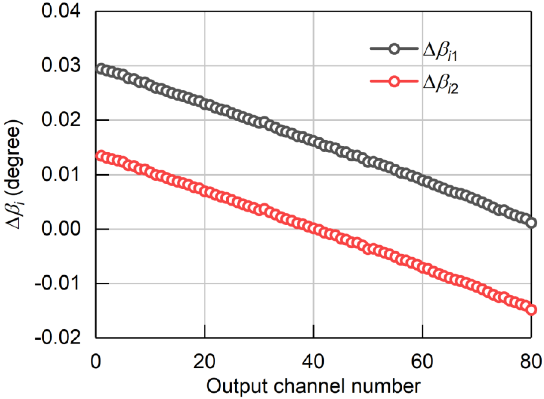
βi2. The change in geometric position for all output waveguides after adjusting
αi can be calculated as Δ
βi1 =
βi2 −
βi1, as shown in
Figure 6.
Given that the output waveguide angular spacing has been determined as
αi2, further optimization of the CFA can only be achieved by adjusting
βi. The angular position of the output waveguides after further adjustments is represented by
βi3. Determining the appropriate value of
βi3 is a procedural task; therefore, employing external codes (such as Matlab, Python, C++, etc.) for simulation and search is a suitable choice.
Figure 7 illustrates the flow diagram for searching
βi3. Initially,
βi3 is incrementally varied with a step size of 0.1 times
αi1, and external codes are utilized to compute and simulate
βi3 in order to determine the sign of the superposed quantity
Σ. Subsequently, the multiplier of
Σ is gradually increased to search for
βi3 based on the desired CFA as the evaluation criterion. Once the CFA requirement of being less than
j times Δ
f is satisfied, the final
βi3 that meets the expected CFA performance indicator is obtained. Here, the value of
j should be less than or equal to 0.1 (in this paper,
j = 0.05). Based on
βi3, Δ
βi2 =
βi3 −
βi2 can be calculated, which represents the variation in the geometric position of all output waveguides after adjusting
βi, as shown in
Figure 6.
5. Results and Discussions
After the adjustment of
αi and
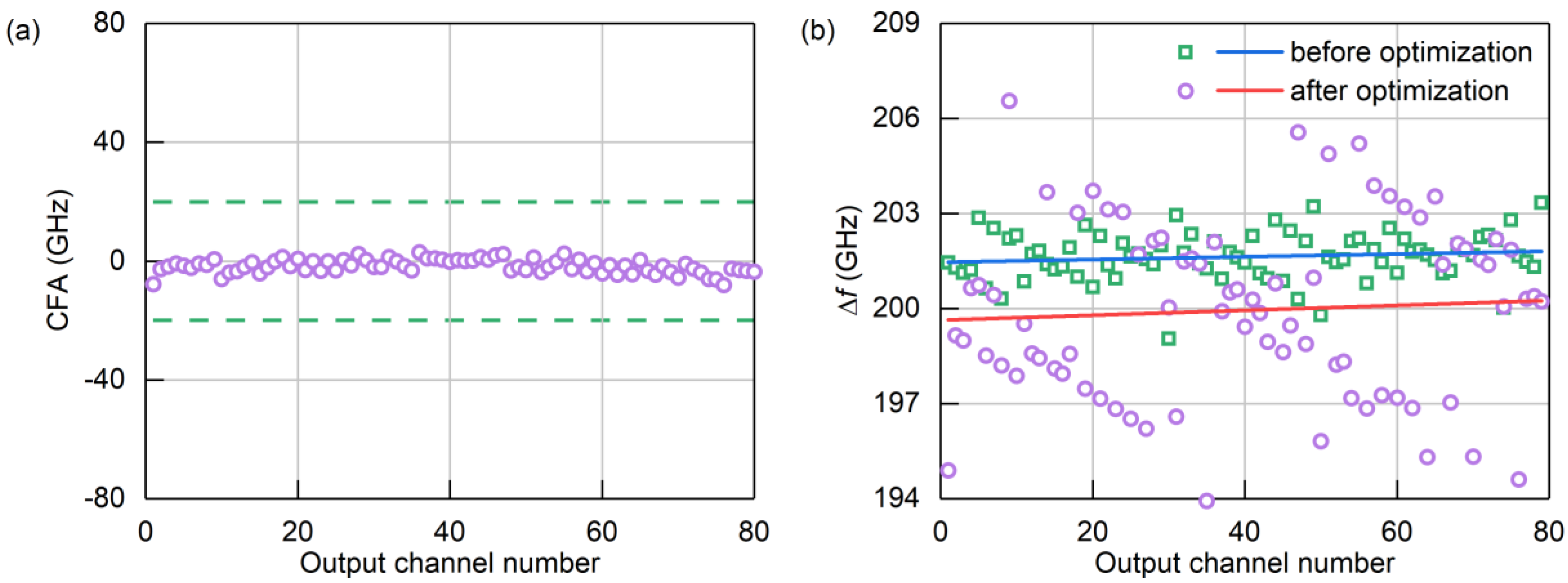
βi, the simulation results of the AWG were analyzed and discussed. The CFA obtained from the optimized simulation is shown in
Figure 8a. In comparison to
Figure 4 and
Figure 5b, it can be observed that the CFA of all output channels is within the range of 20 GHz, indicating a significant improvement in performance.
Figure 8b presents a comparison of the frequency spacing Δ
f for all output channels before and after optimization. Although the values of Δ
f were more concentrated before optimization, the fitted curve reveals that the Δ
f after optimization is closer to 200 GHz. The simulation results demonstrate that the average value of Δ
f before optimization was 201.64 GHz, whereas the average value after optimization was 199.95 GHz. While the values of Δ
f before optimization were concentrated, there was a difference of 1.64 GHz between the average value and 200 GHz, and this discrepancy gradually accumulated towards the output channels located near the edges. According to the simulation results, the value of CFA before optimization was 67.63 GHz. In contrast, the values of Δ
f after optimization, although dispersed, were uniformly distributed around 200 GHz, with a mere 0.05 GHz difference from the average value of 200 GHz. This implies that the edge output channels will not accumulate higher CFA values, leading to a more effective enhancement of the CFA. Based on the simulation results, the value of CFA after optimization was 7.99 GHz.
Figure 9 compares the local spectra of the AWG output before and after CFA optimization. The designed AWG operates within a wavelength range of 600 nm to 620 nm, corresponding to output channels 1−80. By comparing the spectra before and after optimization, it can be observed that the spectra of output channels 1−40 undergo a noticeable red shift after optimization, while the spectra of output channels 41−80 experience a significant blue shift. The output channels closer to the edges exhibit larger shifts in both the red and blue directions. This further confirms the cumulative characteristic of center frequency deviation in the edge channels of high-channel-count AWG in DWDM systems. This negative characteristic poses a critical challenge that needs to be addressed for the expansion and acceleration of DWDM systems. The optimized spectra show no significant upward or downward shifts, apart from the red and blue shifts. Additionally, the shape of the spectra remains nearly unchanged compared to before optimization, indicating that the optimization of CFA does not have a significant impact on the main optical performance of the AWG.
Table 3 presents the main optical performance of the designed AWG after optimization, and
Figure 10 shows the output spectrum of the optimized AWG. It can be observed that the insertion loss, insertion loss uniformity, and adjacent output channel crosstalk essentially remain unchanged and are not affected by the optimization process. Furthermore, the layout design of the AWG in
Figure 3 is also unaffected, with the device size remaining at 19 × 19 mm². The only optical performance that is affected is the CFA, which improves from 67.63 GHz to 7.99 GHz, indicating the effectiveness of the optimization method.
The flow diagram for the CFA optimization method in this study is illustrated in
Figure 11. The overall optimization process can be summarized in four steps. In the first step, the AWG is preliminarily designed following the general design process. In the second step, the main structural parameters are optimized to achieve favorable optical performance indicators. The third step involves adjusting the angular spacing
αi and modifying the constraint relationship of the output waveguides based on Equations (1) and (2). The fourth step utilizes external code in conjunction with device simulation to search for suitable angular positions
βi and adjust the geometric position of the output waveguides. Theoretically, since the AWG simulation allows for infinite subdivision of the operating wavelength range and parameter search using external code, the proposed optimization method can theoretically approach a CFA of 0 GHz. However, in practice, due to limitations in computational resources and time costs, it is generally more appropriate to strike a balance based on the desired performance objectives.
Table 4 presents several different CFA optimization methods. By comparing them, it can be observed that the optimization method proposed in this paper achieves a higher level of CFA, approximately 0.04Δ
f. Two research works based on the Si material platform in the table [
13,
33] demonstrate optimization effects on CFA similar to or even better than this study, but they both involve the addition of extra optical structures. The use of serially connected fiber Bragg grating and parallel AWG significantly increases the device size compared to a single AWG on the same material platform. The research work based on the silica material platform in the table [
35] is also effective, but its optimization method for CFA relies on empirical formulas, lacking sufficient persuasiveness. Optimizing CFA during the AWG design stage and allowing for a sufficient tolerance range is advantageous for reducing center frequency deviations caused by manufacturing errors and operating temperature variations. In addition to silica, the findings of this study are equally applicable to other material platforms. In the future, the research work presented in this paper can be further expanded to include high refractive index differences and even anisotropic material platforms.
