Article

Mask-Shifting-Based Projection Lithography for Microlens Array Fabrication

1
Institute of Optics and Electronics, Chinese Academy of Sciences, Chengdu 610209, China
2
School of Automation Engineering, University of Electronic Science and Technology of China, Chengdu 611731, China
3
University of Chinese Academy of Sciences, Beijing 100049, China
*
Author to whom correspondence should be addressed.
Photonics 2023, 10(10), 1135; https://doi.org/10.3390/photonics10101135
Submission received: 28 July 2023 / Revised: 26 September 2023 / Accepted: 28 September 2023 / Published: 11 October 2023

Abstract

:
Microlens arrays play a critical role in enhancing imaging systems due to their outstanding optical performance, compact size, and lightweight nature. However, traditional fabrication methods for microlens arrays suffer from low precision, inefficiency, high costs, and a lack of adequate surface figure control. In this paper, we present a novel approach for microlens array fabrication, using a projection lithography process with mask-shifting. The method employs a 0.2× projection objective lens to enhance linewidth resolution. By employing a projection-based mask-shift filtering technique, we achieve superior surface figure accuracy while reducing the complexity of mask preparation. The experimental results for four microlenses with different aperture sizes demonstrate surface figure accuracy in the submicron range and surface roughness at the nanometer level. In addition, 3D profilometer scanning equipment was employed to measure the surface roughness of these microlens arrays, and the measurement results of these microlens arrays processed using the proposed method for their surface roughness are 18.4 nm, 29.6 nm, 34.4 nm, and 56.1 nm. Our findings indicate that this method holds great potential in microlens array fabrication, offering the ability to achieve lower linewidths and higher surface figure accuracy compared to conventional methods.

1. Introduction

Micro-optical components play a critical role in the development of miniature and lightweight optical systems. Micro-optical components represented by microlens arrays, with nearly 100% optical diffraction efficiency, excellent dispersion performance, increased degrees of freedom, etc., have been widely used in various fields such as biomedicine, photonics, communications, and sensing [1,2]. With the rapid development of the optoelectronics industry, the feature size of microlens arrays has been reduced to the submicron level, leading to increased difficulty in their fabrication [3,4]. Conventional lithography methods are mainly used for the fabrication of planar two-dimensional (2D) structures, but they cannot meet the high-precision fabrication requirements of microlens arrays. Among them, proximity/contact lithography, as a typical micro/nanofabrication technique, is limited by its resolution and cannot guarantee the submicron accuracy and degrees of freedom [5]. Therefore, an efficient micro/nanofabrication method is crucial for fabricating high-precision microlens arrays.
Currently, existing microlens array fabrication techniques can be mainly divided into maskless and masked lithography. Maskless lithography techniques include direct-write lithography and digital maskless lithography techniques. Direct-write lithography techniques comprise electron beam direct-write lithography [6,7,8], ion beam direct-write lithography [9,10], and two-photon laser direct-write lithography [11,12,13,14,15]. However, these methods suffer from low production efficiency and high processing costs, making them unsuitable for large-scale or large-sized micro-optical component fabrication. The digital maskless lithography techniques for micro-optical component fabrication typically adopt a layer-by-layer slicing approach with multiple exposure processes. This involves extensive slicing operations on the 3D model, where each slicing layer corresponds to one exposure process [16]. Consequently, this method is intricate to execute, and the vertical fabrication accuracy is directly linked to the number of slicing layers, leading to a significant drop in production efficiency.
Masked lithography is a fabrication technique that involves illuminating a mask with homogenized and collimated light to project its pattern onto the substrate surface. Afterward, development and etching processes are used to achieve efficient micro/nanostructure fabrication [17,18]. Various techniques fall under masked lithography, including multilayer binary overlay, nano-imprint, grayscale mask, and lithography with mask-shifting. Multilayer binary lithography relies on discrete step-like structures to approximate continuous surface figure micro-optical components. This method was initially proposed by the Lincoln Laboratory at the Massachusetts Institute of Technology, USA in the late 1980s to manufacture continuous surface figure micro-optical components [19]. However, its application is limited to relatively straightforward focusing lens production, and controlling aberrations poses challenges. Additionally, as the number of steps increases, multiple iterations of lithographic pattern transfer are necessary, leading to prolonged processing cycles, increased costs, and difficulties in achieving precise alignment [20]. Chang et al. [21] introduced a gas-assisted nano-imprint technique for fabricating microlens arrays with a surface roughness below 10 nm. Nonetheless, as a contact lithography approach, this method still faces challenges in terms of alignment accuracy, product yield, and master plate lifespan. It also exhibits certain drawbacks that necessitate optimization, including demolding difficulties, incompatibility with mainstream lithography materials, residual primer issues, and challenges in mask preparation [22]. Mask-shifting technology, as an efficient method for fabricating micro/nano three-dimensional (3D) structures, involves moving the position of a binary mask during the exposure process to achieve continuous modulation of the exposure energy, enabling the fabrication of 3D micro/nanostructures. Dong Xiaochun et al. proposed a mask-shifted fabrication method using proximity/contact lithography equipment. They divided the 3D target structure into numerous fine strip areas and projected the microstructure within each strip area to form a 2D mask subfunction pattern [23,24,25]. Based on this, Axiu Cao et al. conducted research on miniaturized compound eye structures to design and develop a novel multi-dimensional information-detecting compound eye imaging structure [26,27,28]. Shi Lifang et al. proposed an effective method for forming non-spherical microlens arrays using non-periodic lithography with mask-shifting technology [29,30]. These methods have expanded the fabrication scope from simple and regular micro-relief structures to arbitrary continuous surface microstructures, addressing the shaping of micro-optical components with special surface figures and arrangements. However, since most of these methods primarily use proximity/contact exposure systems, their principles limit the minimum aperture size and result in relatively low surface figure accuracy for microlenses, making them unsuitable for mass production and fabrication.
In this study, we propose a projection lithography process with mask-shifting for fabricating microlens arrays with low linewidth and high-precision surface figure accuracy. Projection lithography involves using an imaging system with reduced magnification between the mask and the substrate, ensuring the separation of the mask from the substrate, which improves the linewidth of micro/nanostructures and simplifies mask preparation. Utilizing the mask-shifting technique, the method achieves continuous modulation of exposure energy by adjusting the mask unit pattern and varying the mask movement speed, thereby enhancing the surface figure accuracy of 3D micro/nanostructures. To verify the feasibility and efficiency of the method, microlenses with apertures of 500, 300, 100, and 50 μm were fabricated and compared with the conventional proximity/contact lithography process. The experimental results demonstrate that this method enables lower linewidths, higher precision, and superior performance in microlens array fabrication.

2. Methodology

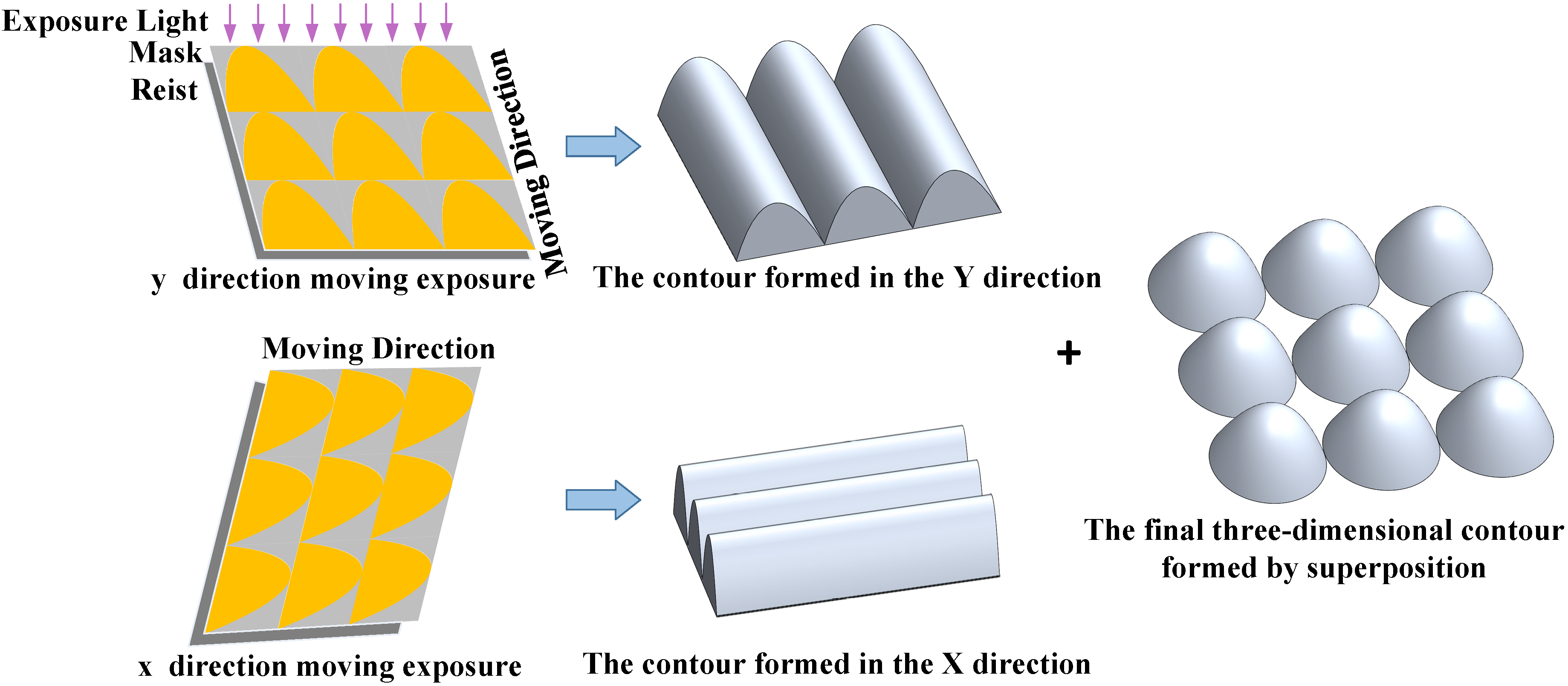
2.1. Mask-Shifting Principle

Projection lithography exposure systems are crucial for micro/nanofabrication, ranging from submicron to deep submicron scales, as they involve projecting the mask’s feature pattern at a reduced magnification onto the substrate surface. Figure 1 illustrates the schematic of a projection lithography system with mask-shifting. The substrate coated with a photoresist is fixed on the 2D moving worktable of the projection exposure system, while the mask is positioned at the mask plane of the projection exposure system. The working principle of the mask-shifted projection exposure system is shown in Figure 1a. The exposure image on the substrate surface is a reduced-size spatial image that is identical to the mask feature pattern, i.e., a series of exposed openings. As the substrate is moved during exposure, the exposed openings are scanned across the substrate surface, achieving a continuous exposure distribution of the feature pattern.
Obtaining a continuous exposure distribution on the substrate surface through mask–substrate relative movement relies on the design of the mask unit pattern and the control of the translation mechanism. Assuming that the mask feature pattern comprises an array of openings, as shown in Figure 1c, during the exposure process, the mask is continuously moved in the Y direction for a period of D. This means that for any point on the mask that moves from point A to point B, the speed of mask movement is v . Therefore, on the substrate surface, the point corresponding to point B undergoes two exposure times t 1 = h 1 / v and t 2 = h 2 / v , and the exposure intensity at that point is
Q ( x , y ) = m 2 I ( x , y ) T ( x , y ) = m 2 I 0 h 1 + h 2 v
where T ( x , y ) is the time of the mask–substrate relative movement during exposure; m is the magnification factor of the projection objective lens; and I ( x , y ) is the exposure intensity transmitted through the mask after modulation, which is a constant and can be expressed by Equation (2)
I ( x , y ) = I 0 White   region   in   the   mask , 0 Black   region   in   the   mask .
where I 0 is the light intensity at the mask surface. Assume that the profile function of the white transparent area within one period of the mask is f ( x ) . Therefore, the accumulated exposure intensity at the position corresponding to point B on the object surface in the projection objective plane can be expressed as
Q ( x , y ) = m 2 I 0 f ( x ) v
Equation (3) defines the exposure intensity on the substrate surface after a single exposure as a function of the coordinate X. Therefore, a single movement can only achieve 2D columnar microstructures.
For 3D periodic, regular structures, they can be achieved through cross-shifted exposure, as shown in Figure 2. After a single movement in the Y direction, the exposure intensity distribution Q y on the substrate surface is given by
Q y ( x , y ) = m 2 I 0 f ( x ) v
After completing the Y direction movement, move along the X direction. The continuous exposure intensity distribution can be expressed as
Q x ( x , y ) = m 2 I 0 f ( y ) v
Thus, on the substrate surface, the final exposure intensity obtained can be defined as
Q ( x , y ) = Q x ( x , y ) + Q y ( x , y ) = m 2 I 0 f ( x ) + f ( y ) v

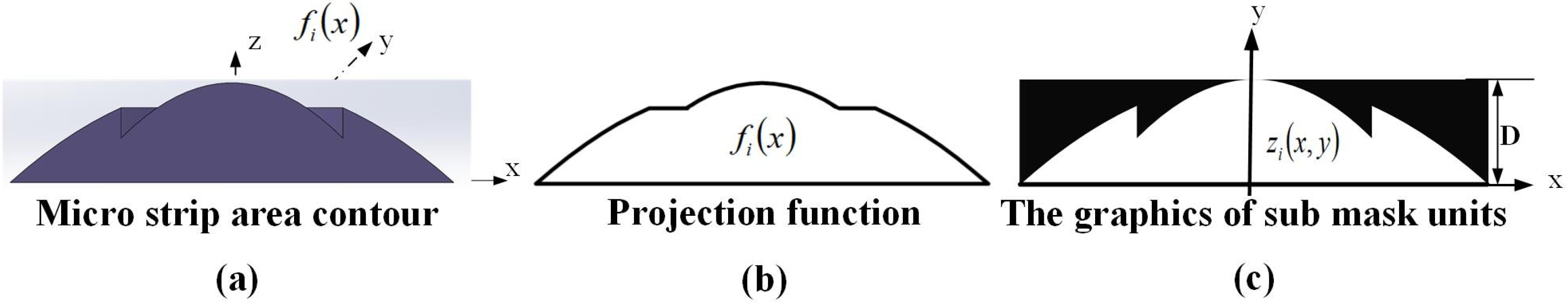
2.2. Mask-Shift Filtering Technique

Theoretically, the mask-shift technique achieves the exposure process of axis-symmetric structures by orthogonal movement. However, the non-completely orthogonal nature of the mask-shift platform introduces orthogonal errors, Δθ during mask movement, resulting in distorted exposure results. Particularly, at submicron and lower nodes, this phenomenon becomes prominent. Taking microlens arrays as an example, the directional deviation caused by orthogonal errors leads to a transformation of the aperture shape from a square to a rhombus or even leads to significant misalignment. To address this issue, we combine lithography with mask-shifting and projection lithography to propose a projection lithography process with mask-shifting for fabricating microlens arrays. In this process, the 3D micro/nanostructures are equally divided into a number of fine strip areas, as shown in Figure 3a, and the microstructures within each strip area are encoded. When the subdivisions of the target structure are sufficiently small, the micro-areas can be approximated as cylindrical, and the 3D micro/nanostructures can be represented by Equation (7) as the mask-shift filtering function.
Figure 3 illustrates the mask-shift filtering process for dividing the target function. In Figure 3a, the 3D structure within the subdivided area is transformed into a 2D curve. Based on this transformation, the mask pattern in each area is obtained, as shown in Figure 3b. These mask patterns in all areas are then sequentially combined to obtain the target function’s shift filtering mask, depicted in Figure 3c.
During the exposure process, the mask is moved at a uniform speed along the subdivision direction of the target function. This movement generates the exposure intensity distribution on the substrate surface by superimposing the exposure intensity distributions generated by the mask encoding units. The ideal exposure profile, sub-mask unit patterns, and micro-strip area’s profile are also shown in Figure 3a.
f i x = i D i + 1 D f i x , y d y ,   i = 0 , 1 , S
where f i x is the 2D projection function of the micro-area, as shown in Figure 3b; y is the horizontal position coordinate of the microstructure; x is its vertical position coordinate; D is the spacing between microstructure subdivisions; S is the number of bar areas; and f i x , y is the exposure profile function within the micro-area.
To obtain the complete shift filtering mask (Figure 3c), multiple columns of mask encoding unit patterns are combined sequentially. The exposure intensity generated by each encoding unit can be expressed as follows:
z i x , y = r e c t y i D f i x / 2 f x i
A number of columns of mask encoding unit patterns are combined sequentially to obtain the complete shift filtering mask (Figure 3c). The exposure intensity generated by each encoding unit can be expressed as
E i x , y = I 0 v z i x , y r e c t ( y i D D / 2 D )
where E i ( x , y ) is the exposure distribution generated by the i-th strip area; z i x , y denotes the mask encoding pattern of the i-th strip area; I 0 is the incident light intensity; v is the mask-shifting speed; denotes the convolution operation; and r e c t ( ) function is the rectangle function. The exposure intensity distribution on the substrate surface is generated by superimposing the exposure intensity distributions generated by the mask encoding units in the moving direction (Figure 3d):
E ( x , y ) = i = 0 S E i ( x , y )
where E ( x , y ) is the exposure intensity distribution on the substrate surface; E i ( x , y ) is the exposure intensity distribution produced by the i-th strip area; and S is the number of strip areas.

2.3. Impact of Mask Preparation Accuracy on the Microstructure’s Surface Figure

In the theoretical analysis, a mask with a series of microstructures can be assumed to be continuous, i.e., z i x , y is a continuous function of the variable x, as shown in Figure 4. However, during the actual mask preparation process, the profile of the strip area is not a continuous function with respect to the variation of x due to the limitations of the mask preparation equipment’s performance. When the microstructure’s subdivision interval D is sufficiently large, the minimum pattern resolution L and the processing accuracy error ΔL of the mask preparation equipment directly determine the quantization order of the projection function f i x within the area D. Therefore, the gray level quantization T of the mask can be expressed as T = ( D 2 L ) / Δ L .
The quantity of the microstructure’s subdivided areas needs to be quantified based on the microstructure’s gray levels. When the quantization interval D of the mask is too small, leading to a significantly higher number of samples compared to the mask’s gray level quantization, i.e., S >> T, most of the pattern areas will have the same gray levels, and the continuity of the pattern is entirely restricted by the number of gray levels as shown in Figure 5a,d.
Based on the gray level quantization, it is evident that the mask’s gray levels primarily depend on the interval D, the mask’s ultimate linewidth L, and processing accuracy ΔL. When determining the mask pattern’s ultimate linewidth, increasing D is the only way to improve the mask’s gray levels. However, if the quantization interval D is too large, leading to much fewer microstructure subdivisions than the mask’s gray level quantization (i.e., S << T), the feature pattern can achieve high continuity in the X direction but becomes highly discrete in the Y direction during mask-shifting. Consequently, the pattern’s continuity is entirely limited by the number of microstructure subdivisions (as shown in Figure 5b,e. When the number of microstructure subdivisions is approximately equal to the mask’s gray levels (i.e., ST), the gray levels and the number of subdivisions will be fully utilized, resulting in optimal continuity of the microstructure formed after mask-shift exposure (as shown in Figure 5c,f). However, for feature sizes in the submicron or below range, existing processing methods fail to meet the accuracy requirements, leading to significant distortion of the microstructure profile. In the proposed method, a 0.2× lithography objective lens is used for exposure imaging. This results in the microstructure profile on the mask surface being 5 times larger than that generated by conventional proximity/contact lithography equipment, i.e., S′ ≈ T′ = 5S ≈ 5T. Consequently, the gray levels of the mask and the number of subdivisions will be fully utilized, and the microstructure formed after mask-shift exposure will achieve superior continuity.

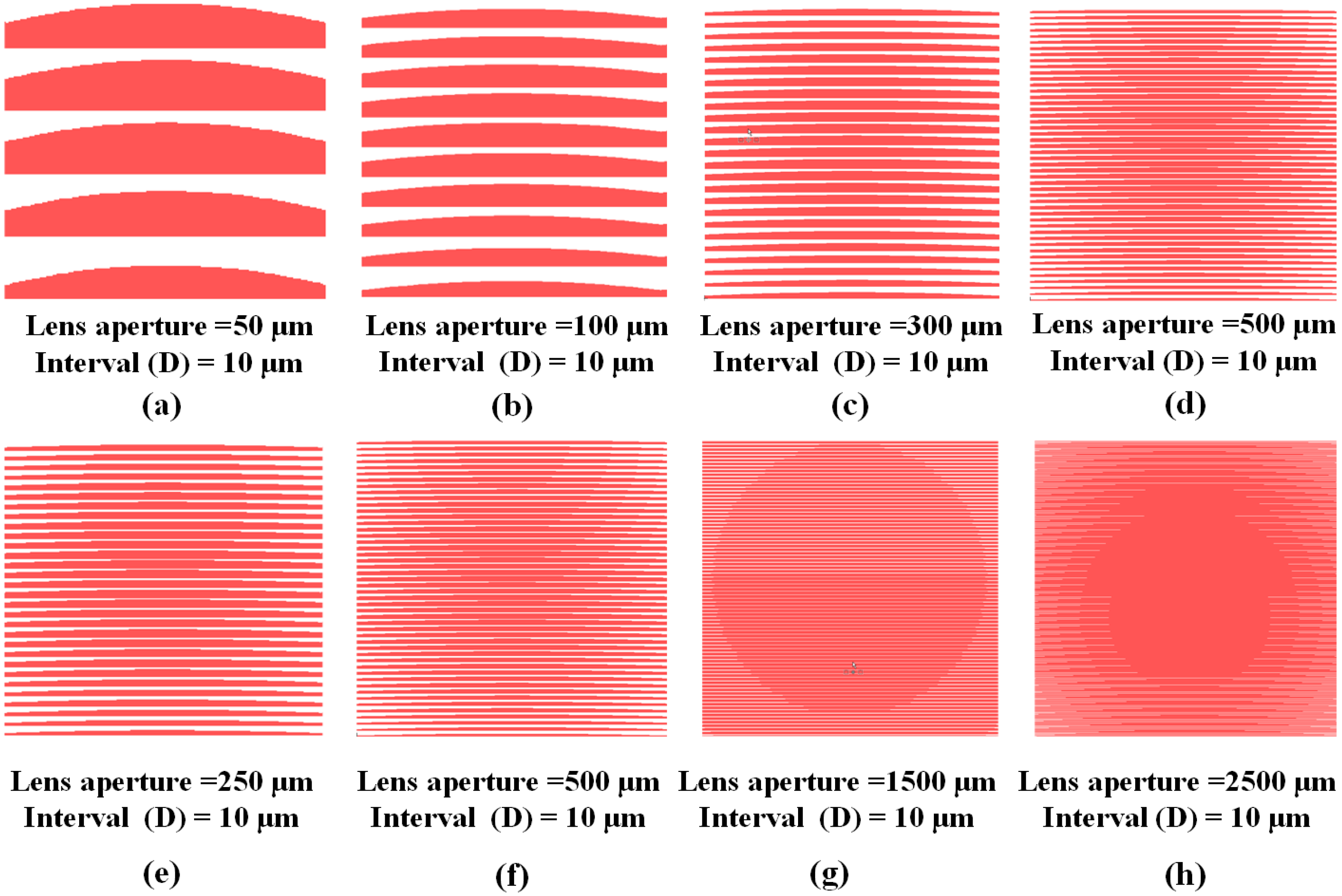
3. Experiment and Analysis

In this study, we used projection lithography equipment to fabricate three-dimensional microstructure devices. The equipment consisted of an illumination system, projection objective lens, alignment system, autofocus system, worktable system, electric control system, software system, and other components. The technical specifications of the equipment include an effective field of view of 15 mm × 15 mm, a numerical aperture of NA = 0.35, an overall optical magnification of M = 1/5×, and a linewidth resolution better than 0.8 µm. To validate the feasibility of the experimental results obtained using the proposed method, we compared it with the conventional proximity/contact lithography method with mask-shifting. In addition, the microlens arrays achieved by these two methods used individual lens apertures of 500, 300, 100, and 50 µm.
Figure 6 shows the two groups’ feature patterns with different characteristics. In the first row, their lens apertures are 50 μm, 100 μm, 300 μm, and 500 μm from (a) to (d), respectively, which were employed in the conventional proximity/contact lithography method. These feature patterns were employed for comparative experiments with the proposed method, and they were divided via 10 μm intervals. Furthermore, these feature patterns, which were utilized to achieve the same aperture lens arrays with the first method by the proposed method, are listed in Figure 6e–h. Due to the advantage of reducing magnification with the projection objective in the proposed method, the dimension of the feature patterns in the second row was five times larger than in the first row. The mask employed in the proposed method is easier to manufacture than the conventional proximity/contact lithography method for achieving the same lens arrays. For controlling external factors to impact the experimental results, these feature patterns were also divided into 10 μm intervals.
As seen in the figure, the proposed mask-shifted projection lithography technique employed a 0.2× lithography objective lens for exposure, resulting in the microstructure profile on the mask surface being five times larger than that generated by the conventional proximity/contact lithography equipment, i.e., S′ ≈ T′ = 5S ≈ 5T. Consequently, the gray levels and the number of subdivisions of the mask were fully utilized. As the aperture of the microlens decreases, the mask design patterns based on projection lithography become more rational and offer greater shaping advantages.
Figure 7 shows the resulting surface figures of four microlenses fabricated using the conventional mask-shift process, while Figure 8 shows the resulting surface figures of four microlenses fabricated using the projection lithography process with mask-shifting. The photoresist used is AZ9260, with a thickness of 4 µm, an exposure dose of 80 mJ/cm2, and a moving speed of 0.825 µm/s. For each microlens aperture size, the fabrication process was repeated three times using both the conventional mask-shift process and the projection lithography process with mask-shifting. The exposed surface figures of the microlenses were measured using a step profiler. The comparison between Figure 7 and Figure 8 demonstrates that the fabrication results from the proposed mask-shift filtering technique based on projection lithography are in good agreement with the simulation results. Moreover, under the same conditions, the proposed method achieves a higher quantization order for mask-shifting compared to the conventional method, resulting in better continuity of the fabricated microstructure devices. On the other hand, the limitations of the conventional proximity/contact lithography equipment led to a decrease in the quantization order as the microlens aperture decreased, resulting in significant discretization of the microstructure profile and, ultimately, the inability to maintain accurate surface figures. Even for the 50 µm aperture microlens (Figure 8d), the proposed projection lithography process with mask-shifting still demonstrated good surface figure fidelity.
To confirm the superiority of the proposed method, the surface results of these microlens arrays processed by the conventional proximity-contact lithography approach and the proposed method were measured using 3D profilometer scanning equipment. The measurement results of microlens arrays for the conventional proximity-contact lithography approach are shown in Figure 9. In this coordinate system, the horizontal axis is represented by the number of pixels. The vertical direction represents the surface height of the microlens arrays. From Figure 9a–d, these measurement results of microlens arrays correspond to the apertures of 500 µm, 300 µm, 100 µm, and 50 µm, respectively. For the different apertures of these microlens arrays, their surface roughness results, measured using 3D profilometer scanning equipment, are 100.4 nm, 158 nm, 263.2 nm, and 396.7 nm, respectively. Figure 10 shows the surface roughness results of these microlens arrays manufactured using the proposed approach, and their measurements do not exceed 60 nm, measuring 18.4 nm, 29.6 nm, 34.4 nm, and 56.1 nm, respectively. The comparison results in Figure 9 and Figure 10 further fully demonstrate that the production results of the proposed approach are consistent with the simulation results. Under the same conditions, the device produced by the mask moving filtering technology based on projection lithography had better continuity. The surface roughness was better than the conventional proximity-contact lithography approach. Through comparison between Figure 9d and Figure 10d, it can be seen that, due to the principal limitations of traditional proximity-contact lithography equipment, as the diameter of the microlens arrays gradually becomes smaller, the patterns exhibit serious discreteness. The surface profile of these lenses cannot be guaranteed. The processing method based on the mask moving filtering technology of projection lithography still has good surface profile shape fidelity.

4. Conclusions

In this study, we proposed a novel method for fabricating microlens arrays using projection lithography and a mask-shifting technique. By combining high-resolution projection lithography with a zoom objective lens, we simplified the mask preparation process, allowing us to fabricate microlens arrays with low linewidth and consistent aperture size. The mask feature pattern was divided into a series of grayscale patterns, effectively converting the microlens array contour into a set of profile functions and reducing the complexity of fabrication. Furthermore, we employed the mask-shift filtering technique, which involved moving the mask in a single direction to achieve continuous modulation of exposure energy, thereby improving the surface figure accuracy of the microlens arrays. To verify the feasibility of our method, we compared the experimental results with those obtained using the conventional proximity/contact lithography technique for microlenses with various aperture sizes, including 500, 300, 100, and 50 µm, and the surface roughness of these microlens arrays was measured using 3D profilometer scanning equipment. The experimental results demonstrated that our proposed method achieved high-fidelity surface figure accuracy, particularly as the microlens aperture size decreased, making it an efficient approach for fabricating microlens arrays.

Author Contributions

Simulation design, J.G.; experiment, J.G. and H.S.; methodology, J.G., H.S. and J.Z.; investigation, J.G, J.Z. and J.L.; data curation, J.G., J.W. and J.Z.; writing—original draft preparation, J.G., J.L. and J.W.; writing—review and editing, J.G., S.H. and J.W. All authors have read and agreed to the published version of the manuscript.

Funding

The work was supported by the National Key Research and Development Plan (2021YFB3200204); the National Natural Science Foundation of China (NSFC) under grant nos. 61604154, 61875201, 61975211, and 62005287; the Youth Innovation Promotion Association of the Chinese Academy of Sciences (2021380); the project of the Western Light of Chinese Academy of Science (YA23K056); and the Sichuan Science and Technology Program (2023JDRC0104).

Institutional Review Board Statement

Not applicable.

Informed Consent Statement

Not applicable.

Data Availability Statement

Not applicable.

Conflicts of Interest

The authors declare no conflict of interest.

References

  1. Dong, X.; Du, C.; Wang, C.; Deng, Q.; Zhang, Y.; Luo, X. Mask-shift filtering for forming microstructures with irregular profile. Appl. Phys. Lett. 2006, 89, 261105. [Google Scholar] [CrossRef]
  2. Dong, X.; Du, C.; Li, S.; Wang, C.; Fu, Y. Control approach for form accuracy of microlenses with continuous relief. Opt. Express 2005, 13, 1353–1360. [Google Scholar] [CrossRef] [PubMed]
  3. Zhang, W.; Zhu, G.; Zhu, X.; Du, C. Ultraprecision replication technology for fabricating spiral-structure metamaterial. Front. Phys. 2020, 8, 555729. [Google Scholar] [CrossRef]
  4. Zhang, W.; Xia, L.; Gao, M.; Du, C. Laser beam homogenization with random distributed freeform cylindrical microlens. Opt. Eng. 2020, 59, 065103. [Google Scholar] [CrossRef]
  5. Zhang, S.; Zhao, L.; He, Y. Lithography alignment method based on image rotation matching. J. Phys. Conf. Ser. 2021, 1939, 012039. [Google Scholar] [CrossRef]
  6. Gopal, V.; Radmilovic, V.R.; Daraio, C.; Jin, S.; Yang, P.; Stach, E.A. Rapid prototyping of site-specific nanocontacts by electron and ion beam assisted direct-write nanolithography. Nano Lett. 2004, 4, 2059–2063. [Google Scholar] [CrossRef]
  7. Bhuvana, T.; Kulkarni, G.U.U. Highly conducting patterned Pd nanowires by direct-write electron beam lithography. ACS Nano 2008, 2, 457–462. [Google Scholar] [CrossRef]
  8. Ekberg, M.; Nikolajeff, F.; Larsson, M.; Hård, S. Proximity-compensated blazed transmission grating manufacture with direct-writing, electron-beam lithography. Appl. Opt. 1994, 33, 103–107. [Google Scholar] [CrossRef]
  9. Lee, L.P.; Berger, S.A.; Liepmann, D.; Pruitt, L. High aspect ratio polymer microstructures and cantilevers for bioMEMS using low energy ion beam and photolithography. Sens. Actuators A 1998, 71, 144–149. [Google Scholar] [CrossRef]
  10. Gonin, Y.; Munnik, F.; Benninger, F.; Mikhaïlov, S. Creating sub-surface channels in PMMA with ion beam lithography in only one step. Appl. Surf. Sci. 2003, 217, 289–293. [Google Scholar] [CrossRef]
  11. Leon, J.A.; Alves, E.S.; Elias, D.C.; Brant, J.C.; Barbosa, T.C.; Malard, L.M.; Pimenta, M.A.; Ribeiro, G.M.; Plentz, F. Rapid fabrication of bilayer graphene devices using direct laser writing photolithography. J. Vac. Sci. Technol. B 2011, 29, 021204. [Google Scholar] [CrossRef]
  12. Xianfan, X. Laser direct write of silicon nanowires. Opt. Eng. 2011, 50, 475–480. [Google Scholar]
  13. Lee, C.H.; Yoshida, H.; Miura, Y.; Fujii, A.; Ozaki, M. Local liquid crystal alignment on patterned micrograting structures photofabricated by two photon excitation direct laser writing. Appl. Phys. Lett. 2008, 93, 173509. [Google Scholar] [CrossRef]
  14. Liu, X.; Chen, Q.; Guan, K.; Ma, Z.; Yu, Y.; Li, Q.; Tian, Z.; Sun, H. Dry-etching-assisted femtosecond laser machining. Laser Photonics Rev. 2017, 11, 1600115. [Google Scholar] [CrossRef]
  15. Liu, X.; Yu, L.; Yang, S.; Chen, Q.; Wang, L.; Juodkazis, S.; Sun, H. Optical Nanofabrication of Concave Microlens Arrays. Laser Photonics Rev. 2019, 13, 1800272. [Google Scholar] [CrossRef]
  16. Liu, J.; Liu, J.; Deng, Q.; Feng, J.; Zhou, S.; Hu, S. Intensity modulation based optical proximity optimization for the maskless lithography. Opt. Express 2020, 28, 548–557. [Google Scholar] [CrossRef]
  17. Artyukov, I.; Balakireva, L.; Bijkerk, F.; Vinogradov, A.; Zorev, N.; Kozhevnikov, I.; Kondratenko, V.; Ogurtsov, O.; Ponomarenko, A.; Fedorenko, A. Projection X-ray-lithography on the basis of oint sources. Kvantovaya Electron. 1992, 19, 114–127. [Google Scholar]
  18. Erdmann, A.; Fühner, T.; Evanschitzky, P.; Agudelo, V.; Freund, C.; Michalak, P.; Xu, D. Optical and EUV projection lithography: A computational view. Microelectron. Eng. 2015, 132, 21–34. [Google Scholar] [CrossRef]
  19. Vlad, A.; Huynen, I.; Melinte, S. Wavelength-scale lens microscopy viathermal reshaping of colloidal particles. Nanotechnology 2012, 23, 285708. [Google Scholar] [CrossRef]
  20. Veldkamp, W.B. Binary optics: A new approach to optical design and fabrication. Opt. News 1988, 14, 29–30. [Google Scholar] [CrossRef]
  21. Chang, C.-Y.; Yang, S.-Y.; Huang, L.-S.; Chang, J.-H. Fabrication of plastic microlens array using gas-assisted micro-hot-embossing with a silicon mold. Infrared Phys. Technol. 2006, 48, 163–173. [Google Scholar] [CrossRef]
  22. Liu, J.; Liu, J.; Deng, Q.; Liu, X.; He, Y.; Tang, Y.; Hu, S. Dose-modulated maskless lithography for the efficient fabrication of compound eyes with enlarged field-of-view. IEEE Photonics J. 2019, 11, 2400110. [Google Scholar] [CrossRef]
  23. Huang, P.; Dong, X.C.; He, C.W. Square-aperture microlens array fabrication by the moving mask technology. In Proceedings of the 2017 2nd International Seminar on Applied Physics, Optoelectronics and Photonics, Lancaster, PA, USA, 2017. [Google Scholar]
  24. Du, C.; Dong, X.; Qiu, C.; Deng, Q.; Zhou, C. Profile control technology for high performance microlens array. Opt. Eng. 2004, 44, 2595–2601. [Google Scholar] [CrossRef]
  25. Du, C.; Dong, X.C.; Deng, Q.; Luo, X. Micro-optical structures formed by a mask moving method. Optoelectron. Lett. 2007, 3, 95–98. [Google Scholar] [CrossRef]
  26. Cao, A.; Wang, J.; Pang, H.; Zhang, M.; Shi, L.; Deng, Q.; Hu, S. Design and fabrication of a multifocal bionic compound eye for imaging. Bioinspir. Biomim. 2018, 13, 026012. [Google Scholar] [CrossRef]
  27. Im, B.; Prasetyo, F.D.; Yudistira, H.T.; Khalil, S.M.; Cho, D.; Byun, D. Drop-on-Demand Electrohydrodynamic Jet Printing of Microlens Array on Flexible Substrates. ACS Appl. Polym. Mater. 2023, 5, 2264–2271. [Google Scholar] [CrossRef]
  28. Zhang, Q.; Schambach, M.; Schlisske, S.; Jin, Q.; Mertens, A.; Rainer, C.; Hernandez-Sosa, G.; Heizmann, M.; Lemmer, U. Fabrication of Microlens Arrays with High Quality and High Fill Factor by Inkjet Printing. Adv. Opt. Mater. 2022, 10, 2200677. [Google Scholar] [CrossRef]
  29. Shi, L.; Du, C.; Dong, X.; Deng, Q.; Luo, X. Effective formation method for an aspherical microlens array based on an aperiodic moving mask during exposure. Appl. Opt. 2007, 46, 8346–8350. [Google Scholar] [CrossRef]
  30. Li, Q.; Ji, M.G.; Chapagain, A.; Cho, I.H.; Kim, J. Curvature-Adjustable Polymeric Nanolens Fabrication Using UV-Controlled Nanoimprint Lithography. Micromachines 2022, 13, 2183. [Google Scholar] [CrossRef]
Figure 1. (a) Mask-shift principle; (b) mask-shifted pattern; and (c) working principle of the mask-shifted projection exposure system.
Photonics 10 01135 g001
Figure 2. Principle of two-crossed mask-shifted exposure.
Photonics 10 01135 g002
Figure 3. Principle of the mask moving filter method: (a) the equally divided objective function; (b) the microstrip area outline function; (c) the divided feature pattern; and (d) the moving filter mask.
Photonics 10 01135 g003
Figure 4. Sub-mask encoding unit pattern: (a) micro-strip area’s profile; (b) projection function; and (c) graphics of the sub-mask units.
Photonics 10 01135 g004
Figure 5. (a) Microstructure recovered using the mask-shift filtering technique when S >> T. (b) Microstructure recovered using the mask-shift filtering technique when S << T. (c) Microstructure recovered using the mask-shift filtering technique when ST. (d) Mask design 2D graphics when S >> T. (e) Mask design 2D graphics when S << T. (f) Mask design 2D graphics when ST.
Photonics 10 01135 g005
Figure 6. Mask specifications for the two experimental methods. (ad) different feature patterns for the conventional proximity/contact lithography method; (eh) different feature patterns for the proposed method. For the conventional proximity/contact lithography method, the lens apertures of the four feature patterns are respectively 50 μm, 100 μm, 300 μm, and 500 μm; and for the proposed method, their apertures are 250 μm, 500 μm, 1500 μm, and 2500 μm, respectively.
Photonics 10 01135 g006
Figure 7. Resulting microlens’ surface figures based on the conventional mask-shift process: (a) surface figure measurements of the 500 µm aperture; (b) surface figure measurements of the 300 µm aperture; (c) surface figure measurements of the 100 µm aperture; and (d) surface figure measurements of the 50 µm aperture.
Photonics 10 01135 g007
Figure 8. Resulting microlens’ surface figures based on the projection lithography process with mask-shifting: (a) surface figure measurements of the 500 µm aperture; (b) surface figure measurements of the 300 µm aperture; (c) surface figure measurements of the 100 µm aperture; and (d) surface figure measurements of the 50 µm aperture.
Photonics 10 01135 g008
Figure 9. Surface results of microlens arrays measured via the 3D profilometer scanning method using the conventional proximity-contact lithography approach. (ad) Results of the 3D profilometer scanning measurements for the different apertures: 500 µm, 300 µm, 100 µm, and 50 µm, respectively.
Photonics 10 01135 g009
Figure 10. Surface results of microlens arrays measured via the 3D profilometer scanning method using the proposed approach. (ad) Results of the 3D profilometer scanning measurements for the different apertures: 500 µm, 300 µm, 100 µm, and 50 µm, respectively.
Photonics 10 01135 g010
Disclaimer/Publisher’s Note: The statements, opinions and data contained in all publications are solely those of the individual author(s) and contributor(s) and not of MDPI and/or the editor(s). MDPI and/or the editor(s) disclaim responsibility for any injury to people or property resulting from any ideas, methods, instructions or products referred to in the content.

