Improvement of Power and Efficiency of High-Mesa Semi-Insulating InP: Fe Buried Heterostructure Lasers with Wide Bandgap Layers

 , , ,
, , ,
Abstract
:1. Introduction
2. Trap Models and Laser Configurations
2.1. Deep-Level Traps for SI Material
2.2. Configuration for SIBH Lasers
3. Simulation Results
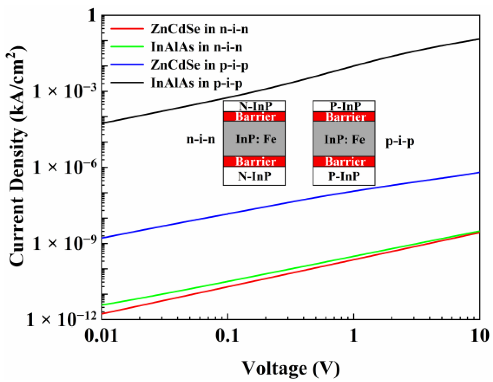
3.1. Analysis of Leakage Current Mechanism
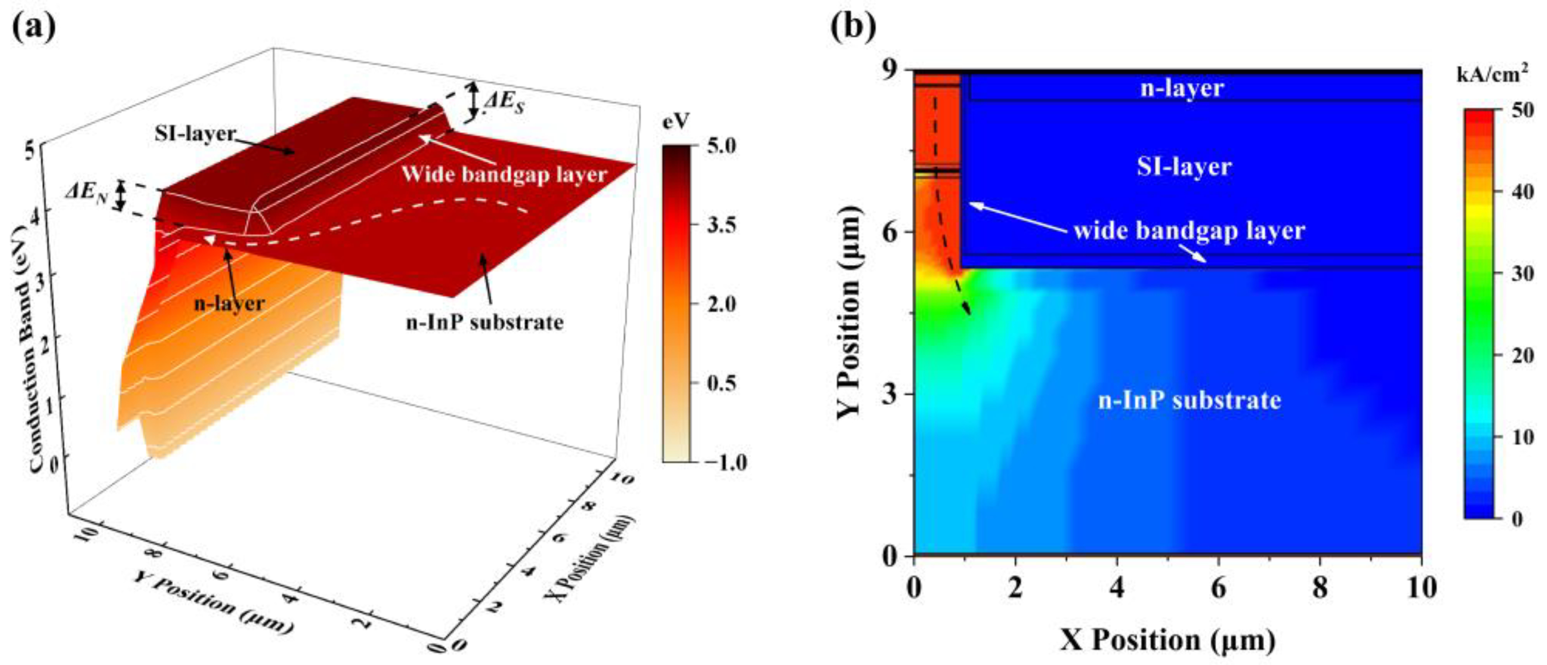
3.2. SIBH Lasers with Wide Bandgap Layers
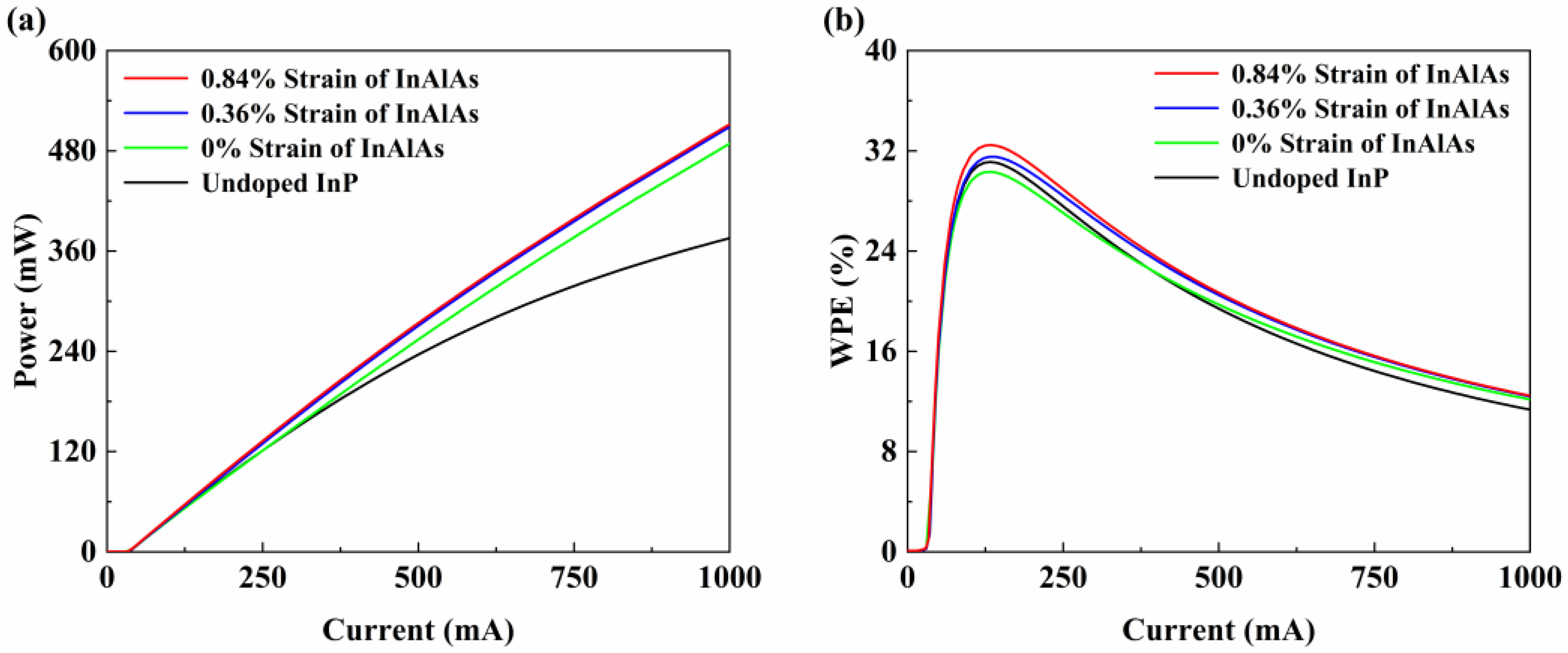
3.2.1. SIBH Lasers with InAlAs Layers
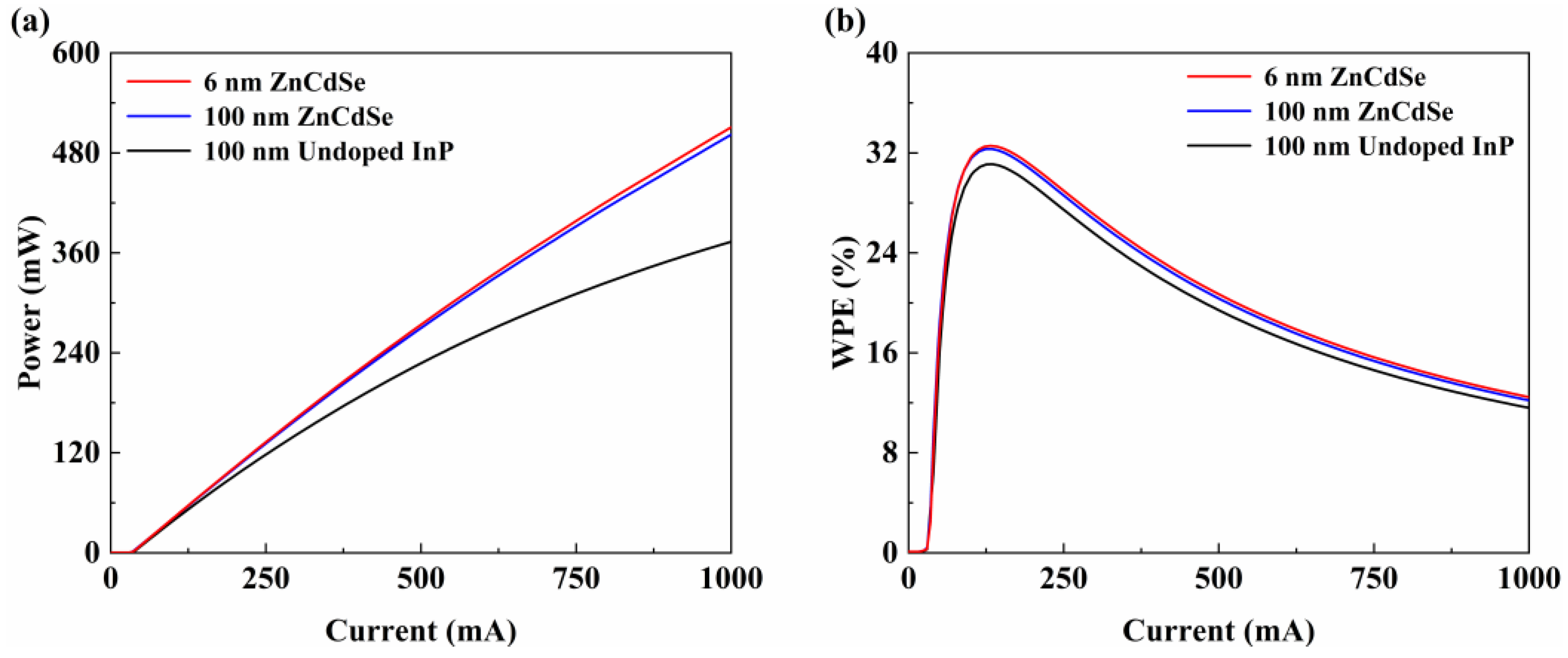
3.2.2. SIBH Lasers with ZnCdSe Layers
3.2.3. The Role of Wide Bandgap Layers
4. Discussion
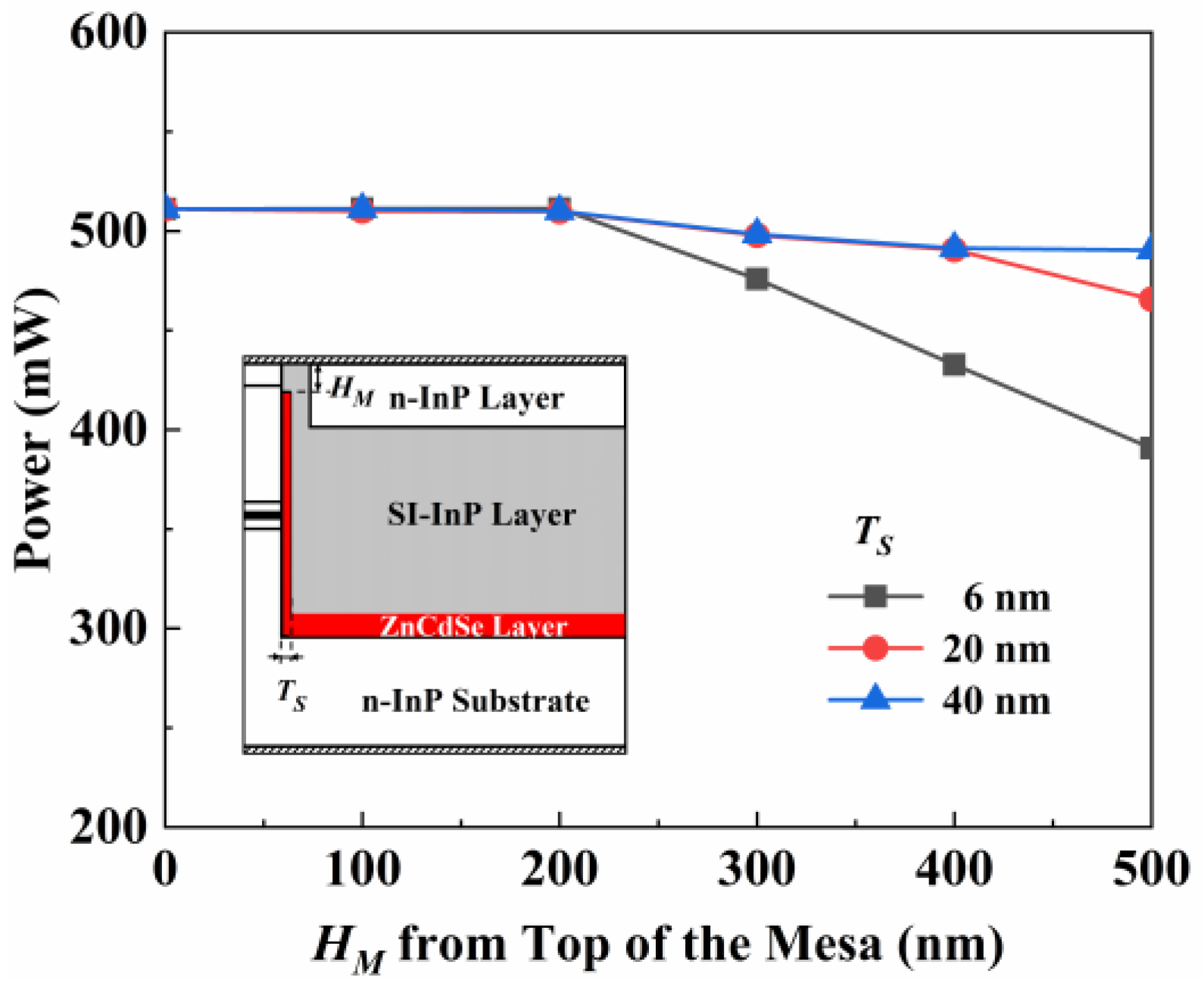
4.1. Suitable Thickness for Wide Bandgap Layers
4.2. The Effect of Mesa Profiles on Output Characteristics
5. Conclusions
Author Contributions
Funding
Institutional Review Board Statement
Informed Consent Statement
Data Availability Statement
Conflicts of Interest
Appendix A

| Parameter | Value |
|---|---|
| Intraband Relaxation Time (ps) | 0.1 |
| Gain Compression Factor (cm3) | 5 × 10⁻¹⁷ |
| Bandgap Renormalization Coefficient (eV·cm) | 1 × 10⁻⁸ |
| SRH Recombination Lifetime (ns) | 20 (In active region), 100 (In passive region) |
| Spontaneous Emission Parameter (cm3·s−1) | 1 × 10⁻¹⁰ |
| Auger Parameter (cm6·s−1) | 0 (For electrons), 1.6 × 10⁻²⁸ (For holes) |
| Free Carrier Absorption Coefficient (cm2) | 10−18 (For electrons), 35 × 10−18 (For holes in active region), 20 × 10−18 (For holes in passive region) |
| Parameter | Thickness (nm) | Doping (cm−3) |
|---|---|---|
| P-In0.53Ga0.47As contact layer | 200 | 1 × 10¹⁹ |
| P-In0.78Ga0.22As0.47P0.53 transition layer | 30 | 1.5 × 10¹⁸ |
| P-InP cladding layer | 1200 | 1.5 × 10¹⁸ |
| P-InP cladding layer | 200 | 1 × 10¹⁸ |
| P-InP cladding layer | 100 | 5 × 10¹⁷ |
| In0.82Ga0.18As0.4P0.6 SCH layer | 100 | Unintentional doping |
| In0.78Ga0.22As0.8P0.2 well | 6.5 | Unintentional doping |
| In0.66Ga0.34As0.61P0.39 barrier | 9 | Unintentional doping |
| In0.82Ga0.18As0.4P0.6 SCH layer | 100 | Unintentional doping |
| N-InP cladding layer | 1500 | 1 × 10¹⁸ |
| N-InP substrate | 5000 | 2 × 10¹⁸ |
References
- Nakahara, K.; Wakayama, Y.; Kitatani, T.; Taniguchi, T.; Fukamachi, T.; Sakuma, Y.; Tanaka, S. 80 °C, 50-Gb/s Directly Modulated InGaAlAs BH-DFB Lasers. In Proceedings of the 2014 International Semiconductor Laser Conference, Palma de Mallorca, Spain, 7–10 September2014. [Google Scholar]
- Yokokawa, S.; Nakamura, A.; Hamada, S.; Nakajima, R.; Okamoto, K.; Arasawa, M.; Nakahara, K.; Tanaka, S. Over 100 mW Uncooled Operation of SOA-integrated 1.3-μm Highly Reliable CW-DFB Laser. In Proceedings of the 2022 Optical Fiber Communications Conference and Exhibition (OFC), San Diego, CA, USA, 6–10 March 2022. [Google Scholar]
- Takeshita, T.; Tadokoro, T.; Iga, R.; Tohmori, Y.; Yamamoto, M.; Sugo, M. Highly Reliable 1.5 μm DFB Laser with High-Mesa SIBH Structure. IEEE Trans. Electron Devices 2007, 54, 456–461. [Google Scholar] [CrossRef]
- Asada, S.; Sugou, S.; Kasahara, K.; Kumashiro, S. Analysis of leakage current in buried heterostructure lasers with semiinsulating blocking layers. IEEE J. Quantum Electron. 1989, 25, 1362–1368. [Google Scholar] [CrossRef]
- Yoshida, Y.; Watanabe, H.; Shibata, K.; Takemoto, A.; Higuchi, H. Theoretical and experimental analysis of leakage current in InGaAsP BH lasers with p-n-p-n current blocking layers. IEEE J. Quantum Electron. 1999, 35, 1332–1336. [Google Scholar] [CrossRef]
- Amann, M.C.; Thulke, W. Current confinement and leakage currents in planar buried-ridge-structure laser diodes on n-substrate. IEEE J. Quantum Electron. 1989, 25, 1595–1602. [Google Scholar] [CrossRef]
- Kwon, O.K.; Lee, C.W.; Leem, Y.A.; Kim, K.S.; Oh, S.H.; Nam, E.S. 1.5-μm and 10-Gb s−1 etched mesa buried heterostructure DFB-LD for datacenter networks. Semicond. Sci. Technol. 2015, 30, 105010. [Google Scholar] [CrossRef]
- Söderström, D.; Lourdudoss, S. Resistivity analysis on n-semi-insulating-n and p-semi-insulating-p structures exemplified with semi-insulating InP. J. Appl. Phys. 2001, 89, 4004–4009. [Google Scholar] [CrossRef]
- Young, E.W.A.; Fontijn, G.M.; Vriezema, C.J.; Zalm, P.C. An effective barrier against the interdiffusion of iron and zinc dopants in InP. J. Appl. Phys. 1991, 70, 3593–3599. [Google Scholar] [CrossRef]
- Kim, H.-S.; Oh, D.; Choi, I.-H. Effect of p-doping profile on performance of strained InGaAs/InGaAsP multiple quantum well buried heterostructure laser diodes with Fe or p/n/p-doped InP current blocking layer. Mater. Sci. Eng. B Solid State Mater. Adv. Technol. 2000, 77, 202–206. [Google Scholar] [CrossRef]
- Ogasawara, M.; Iga, R.; Yamanaka, T.; Kondo, S.; Kondo, Y. Correlation between Fe–Zn Interdiffusion Observed by Scanning Capacitance Microscopy and Device Characteristics of Electro-Absorption Modulators. Jpn. J. Appl. Phys. 2003, 42, 2320. [Google Scholar] [CrossRef]
- Thijs, P.J.A.; Binsma, J.J.M.; Young, E.W.A.; van Gils, W.M.E. High power and high temperature operation of 1.5 μm wavelength strained-layer InGaAs/InGaAsP SIPBH lasers. In Proceedings of the Third International Conference Indium Phosphide and Related Materials, Cardiff, UK, 8–11 April 1991. [Google Scholar]
- van Geelen, A.; Binsma, J.J.M.; van Dongen, T.; van Leerdam, A.; Dadger, A.; Bimberg, D.; Stenzel, O.; Schumann, H. Ruthenium doped high power 1.48 μm SIPBH laser. In Proceedings of the Eleventh International Conference on Indium Phosphide and Related Materials, Davos, Switzerland, 16–20 May 1999. [Google Scholar]
- Bouadma, N.; Kazmierski, C.; Semo, J. Over 245 mW 1.3 μm buried ridge stripe laser diodes on n-substrate fabricated by the reactive ion beam etching technique. Appl. Phys. Lett. 1991, 59, 22–24. [Google Scholar] [CrossRef]
- Ohtoshi, T.; Chinone, N. Suppression of leakage current in InGaAsP/InP buried heterostructure lasers by InAlAs strained current-blocking layers. Electron. Lett. 1991, 27, 12–13. [Google Scholar] [CrossRef]
- Murrell, D.L.; Young, R.E. Improvement of the high-temperature performance of 1.3 mu m buried heterostructure lasers by the use of an AlInAs layer to limit current leakage. Semicond. Sci. Technol. 1993, 8, 1662–1665. [Google Scholar] [CrossRef]
- Kushibe, M.; Takaoka, K. New selective metalorganic chemical vapor deposition growth method for InAlAs with high aluminum composition. J. Cryst. Growth 1994, 145, 263–270. [Google Scholar] [CrossRef]
- Kimura, T.; Ochi, S.; Ishida, T.; Ishimura, E.; Sonoda, T.; Mihashi, Y.; Takamiya, S.; Susaki, W. Undoped Al0.48In0.52As grown by metalorganic chemical vapor deposition as the current-blocking layer of laser diodes. J. Cryst. Growth 1996, 158, 418–424. [Google Scholar] [CrossRef]
- Bouchoule, S.; Decobert, J.; Grosmaire, S.; Leclerc, D.; Kazmierski, C. Low-capacitance laser heterostructure selectively buried in SI-InAlAs by AP-MOVPE. In Proceedings of the 27th European Conference on Optical Communication (Cat. No.01TH8551), Amsterdam, The Netherlands, 30 September–4 October 2001. [Google Scholar]
- Vasil’ev, M.G.; Vasil’ev, A.M.; Izotov, A.D.; Marenkin, S.F.; Pashkova, O.N.; Shelyakin, A.A. Fabrication of ZnSe/InP Heterojunctions on Flat and Shaped Surfaces of InP Laser Crystals. Inorg. Mater. 2019, 55, 903–907. [Google Scholar] [CrossRef]
- Kimura, T.; Ochi, S.; Fujii, N.; Ishida, T.; Sonoda, T.; Takamiya, S.; Mitsui, S. High resistivity undoped Al0.48In0.52As layers grown by low-temperature metalorganic chemical vapor deposition. J. Cryst. Growth 1994, 145, 963–967. [Google Scholar] [CrossRef]
- Hofmann, D.; Müller, G.; Streckfuß, N. Semi-insulating electrical properties of undoped inp after heat treatment in a phosphorus atmosphere. Appl. Phys. A 1989, 48, 315–319. [Google Scholar] [CrossRef]
- Yang, H.; Wang, H.; Radhakrishnan, K.; Tan, C.-L. Thermal resistance of metamorphic InP-based HBTs on GaAs substrates using a linearly graded In/sub x/Ga/sub 1-x/P metamorphic buffer. IEEE Trans. Electron Devices 2004, 51, 1221–1227. [Google Scholar] [CrossRef]
- Strzałkowski, K.; Abouais, A.; Alaoui-Belghiti, A.; Singh, D.; Hajjaji, A. Alloy Disordering Effects on the Thermal Conductivity and Energy Gap Temperature Dependence of Cd1−xZnxSe Ternary Crystals Grown by the Bridgman Method. Materials 2023, 16, 3945. [Google Scholar] [CrossRef]
- Kumar, V.; Sastry, B.S.R. Thermal Expansion Coefficient of Binary Semiconductors. Cryst. Res. Technol. 2001, 36, 565–569. [Google Scholar] [CrossRef]
- Barrios, C.A.; Lourdudoss, S.; Martinsson, H. Analysis of leakage current in GaAs/AlGaAs buried-heterostructure lasers with a semi-insulating GaInP:Fe burying layer. J. Appl. Phys. 2002, 92, 2506–2517. [Google Scholar] [CrossRef]
- Corvini, P.J.; Bowers, J.E. Model for trap filling and avalanche breakdown in semi-insulating Fe:InP. J. Appl. Phys. 1997, 82, 259–269. [Google Scholar] [CrossRef]
- Ducroquet, F.; Guillot, G.; Hong, K.; Hong, C.H.; Pavlidis, D.; Gauneau, M. Deep Level Characterization of Lp-Mocvd Grown Al0.48In0.52As. MRS Online Proc. Libr. 1993, 325, 235–239. [Google Scholar] [CrossRef]
- Lourdudoss, S.; Kjebon, O. Hydride vapor phase epitaxy revisited. IEEE J. Quantum Electron. 1997, 3, 749–767. [Google Scholar] [CrossRef]
- Tsang, W.T.; Sudbo, A.S.; Yang, L.; Camarda, R.; Leibenguth, R.E. Iron-doped semi-insulating InP grown by chemical beam epitaxy. Appl. Phys. Lett. 1989, 54, 2336–2338. [Google Scholar] [CrossRef]
- Piprek, J. Advanced analysis of high-temperature failure mechanisms in telecom lasers. In Proceedings of the Conference on Semiconductor Lasers for Lightwave Communication Systems, Denver, CO, USA, 21–22 August 2001. [Google Scholar]
- Ishutkin, S.; Arykov, V.; Yunusov, I.; Stepanenko, M.; Smirnov, V.; Troyan, P.; Zhidik, Y. The Method of Low-Temperature ICP Etching of InP/InGaAsP Heterostructures in Cl2-Based Plasma for Integrated Optics Applications. Micromachines 2021, 12, 1535. [Google Scholar] [CrossRef]
- Zilko, J.L.; Segner, B.P.; Chakrabarti, U.K.; Logan, R.A.; Lopata, J.; Van Haren, D.L.; Long, J.A. Effect of mesa shape on the planarity of InP regrowths performed by atmospheric pressure and low pressure selective metalorganic vapor phase epitaxy. J. Cryst. Growth 1991, 109, 264–271. [Google Scholar] [CrossRef]
- Takemi, M.; Kimura, T.; Suzuki, D.; Shiba, T.; Shibata, K.; Mihashi, Y.; Takamiya, S.; Aiga, M. MOCVD regrowth of InP on RIE patterned substrates for p-substrate 1.3 μm BH laser application. In Proceedings of the 8th International Conference on Indium Phosphide and Related Materials, Schwaebisch-Gmuend, Germany, 21–25 April 1996. [Google Scholar]
- Wolf, T.; Zinke, T.; Krost, A.; Scheffler, H.; Ullrich, H.; Bimberg, D.; Harde, P. Fe and Ti doping of InP grown by metalorganic chemical-vapor deposition for the fabrication of thermally stable high-resistivity layers. J. Appl. Phys. 1994, 75, 3870–3881. [Google Scholar] [CrossRef]
- Loualiche, S.; Ginudi, A.; Le Corre, A.; Lecrosnier, D.; Vaudry, C.; Henry, L.; Guillemot, C. Pseudomorphic GaInP Schottky diode and high electron mobility transistor on InP. Appl. Phys. Lett. 1989, 55, 2099–2101. [Google Scholar] [CrossRef]
- Hadj Belgacem, C.; Fnaiech, M. Solution for the critical thickness models of dislocation generation in epitaxial thin films using the Lambert W function. J. Mater. Sci. 2011, 46, 1913–1915. [Google Scholar] [CrossRef]
- Lee, S.T.; Lee, I.-G.; Jang, H.; Kong, M.; Song, C.; Kim, C.Z.; Jung, S.H.; Choi, Y.; Kim, S.; Eom, S.-k.; et al. High performance InGaAs channel MOSFETs on highly resistive InAlAs buffer layers. Solid-State Electron. 2021, 176, 107940. [Google Scholar] [CrossRef]
- Smith, B.L.; Hoven, N.M.; Hillier, G.; Hubbard, S.M.; Forbes, D.V. OMVPE of InAlAs Using Alternative Al and As Precursors. MRS Online Proc. Libr. 2014, 1635, 63–68. [Google Scholar] [CrossRef]
- Kishino, K.; Nomura, I. II-VI semiconductors on InP for green-yellow emitters. IEEE J. Sel. Top. Quantum Electron. 2002, 8, 773–786. [Google Scholar] [CrossRef]
- Won, H.-K.; Hark, S.K. MOCVD growth of ZnCdSe on InP (001) substrates. MRS Online Proc. Libr. 1996, 441, 199–204. [Google Scholar] [CrossRef]
- Nida, S.; Hinkov, B.; Gini, E.; Faist, J. Characterization of iron doped indium phosphide as a current blocking layer in buried heterostructure quantum cascade lasers. J. Appl. Phys. 2017, 121, 094502. [Google Scholar] [CrossRef]
- Liu, X.; Furdyna, J.K. Optical dispersion of ternary II–VI semiconductor alloys. J. Appl. Phys. 2004, 95, 7754–7764. [Google Scholar] [CrossRef]
- Muñoz, M.N.; Lu, H.; Zhou, X.; Tamargo, M.C.; Pollak, F.H. Band offset determination of Zn0.53Cd0.47Se/Zn0.29Cd0.24Mg0.47Se. Appl. Phys. Lett. 2003, 83, 1995–1997. [Google Scholar] [CrossRef]


| Ref. | Material | Bandgap | Lattice Constant | Resistivity | Crystalline | Thermal Conductivity | Thermal Expansion Coefficient c |
|---|---|---|---|---|---|---|---|
| [4] | In0.5Ga0.5P | 1.87 eV | 5.66 Å | Single-crystalline | 15.7 W/(m·K) a | 5.8 × 10⁻⁶ K−1 | |
| [21] | In0.52Al0.48As | 1.47 eV | 5.87 Å | 2 × 10⁸ Ω·cm | Single-crystalline | 5.7 W/(m·K) a | 4.1 × 10⁻⁶ K−1 |
| [13] | In0.46Al0.54As | 1.63 eV | 5.84 Å | Single-crystalline | 5.8 W/(m·K) a | 4.0 × 10⁻⁶ K−1 | |
| [20] | ZnSe | 2.7 eV | 5.67 Å | 108 Ω·cm | Polycrystalline | 17.3 W/(m·K) b | 7.7 × 10⁻⁶ K−1 |
| [22] | SI InP: Fe | 1.35 eV | 5.87 Å | 107 Ω·cm | Single-crystalline | 68 W/(m·K) | 5.5 × 10⁻⁶ K−1 |
| SiO2 | 9 eV | 1014 Ω·cm | Amorphous | 1.4 W/(m·K) | 0.5 × 10⁻⁶ K−1 | ||
| This work | Zn0.48Cd0.52Se | 2.08 eV | 5.87 Å | Single-crystalline | 2 W/(m·K) b | 7.5 × 10⁻⁶ K−1 |
| Parameter | Fe | O |
|---|---|---|
| Trap type | Deep acceptor in InP | Deep acceptor in InAlAs |
| Trap level (eV) | 0.59 a | 0.6 c |
| Electron capture cross section (cm2) | 3 × 10⁻¹⁵ a | 5 × 10⁻¹⁴ c |
| Hole capture cross section (cm2) | 1 × 10⁻¹⁶ a | 5 × 10⁻¹⁴ c |
| Trap density (cm−3) | 8 × 10¹⁶ b | 2 × 10¹⁶ c |
| Parameter | Value | Parameter | Value |
|---|---|---|---|
| Refractive index | 2.48 @ 1550 nm a | Electron mobility (m2·V−1·s−1) | 0.1~0.6 c |
| Bandgap (eV) | 2.08 b | Hole mobility (m2·V−1·s−1) | 0.04~0.08 c |
| Electron effective mass | 0.13 b | Affinity (eV) | 3.82 c |
| Hole effective mass | 0.56 b | Absorption (m−1) | 0 c |
| Inclination Angle of the Mesa | Active Region Width | Power | WPE | Horizontal Angle | Vertical Angle |
|---|---|---|---|---|---|
| 90° (Vertical Sidewall) | 2 μm | 510.7 mW | 12.4% | 33° | 35° |
| 80° | 2.64 μm | 525.5 mW | 14.0% | 28° | 35.5° |
| 70° | 3.35 μm | 535.0 mW | 15.2% | 24° | 36° |
| 60° | 4.14 μm | 550.1 mW | 16.3% | 20.4° | 37° |
Disclaimer/Publisher’s Note: The statements, opinions and data contained in all publications are solely those of the individual author(s) and contributor(s) and not of MDPI and/or the editor(s). MDPI and/or the editor(s) disclaim responsibility for any injury to people or property resulting from any ideas, methods, instructions or products referred to in the content. |
© 2023 by the authors. Licensee MDPI, Basel, Switzerland. This article is an open access article distributed under the terms and conditions of the Creative Commons Attribution (CC BY) license (https://creativecommons.org/licenses/by/4.0/).
Share and Cite
Lyu, C.; Zhou, X.; Yu, H.; Wang, M.; Zhang, Y.; Pan, J. Improvement of Power and Efficiency of High-Mesa Semi-Insulating InP: Fe Buried Heterostructure Lasers with Wide Bandgap Layers. Photonics 2023, 10, 1094. https://doi.org/10.3390/photonics10101094
Lyu C, Zhou X, Yu H, Wang M, Zhang Y, Pan J. Improvement of Power and Efficiency of High-Mesa Semi-Insulating InP: Fe Buried Heterostructure Lasers with Wide Bandgap Layers. Photonics. 2023; 10(10):1094. https://doi.org/10.3390/photonics10101094
Chicago/Turabian StyleLyu, Chen, Xuliang Zhou, Hongyan Yu, Mengqi Wang, Yejin Zhang, and Jiaoqing Pan. 2023. "Improvement of Power and Efficiency of High-Mesa Semi-Insulating InP: Fe Buried Heterostructure Lasers with Wide Bandgap Layers" Photonics 10, no. 10: 1094. https://doi.org/10.3390/photonics10101094
APA StyleLyu, C., Zhou, X., Yu, H., Wang, M., Zhang, Y., & Pan, J. (2023). Improvement of Power and Efficiency of High-Mesa Semi-Insulating InP: Fe Buried Heterostructure Lasers with Wide Bandgap Layers. Photonics, 10(10), 1094. https://doi.org/10.3390/photonics10101094