1. Introduction
Color, the main carrier of visual information in nature, takes on a critical significance to daily life. The transmission mode of human information has been fundamentally changed with the application of color display. Over the past few years, thin-film display technology with high resolution has aroused wide attention [
1,
2,
3,
4]. In general, principles of conventional color display film have been currently classified into three types as follows: (1) surface plasmons are formed from photographed nanocolumns for color display [
5]. The patterns produced by the surface plasmon technique exhibit significantly low color saturation, while the surface metals are inevitably dependent on angles. (2) High saturation color is achieved through multilayer multi-polarization modulation [
6]. Multi-polarization modulation has been primarily adopted to suppress the non-resonant wavelength of multilayer films via the matching of refractive index between layers. The multi-polarization modulation structure exhibits a wide color gamut and high monochromatic property. Lithography is required for the preparation of this structure, and the color cannot be changed after the structure is formed. (3) The F–P cavity structure based on the strong interference effect exhibits high compatibility and flexible application [
7], while it is seriously dependent on angles and has weak monochromatic display ability. Based on existing technology, color display of highly monochromatic structures is dependent on lithography, thus significantly increasing the cost of use; once the structure color is fixed, it cannot be changed. To solve the above problem, a photoelectric framework using non-volatile phase change materials (PCMs) was proposed by Hosseini [
8]. Under the stimulation of light, electricity, and heat, PCMs are capable of rapidly converting two types of solid state (crystal state and amorphous state), and this conversion is reversible [
9,
10,
11]. In the conversion process, the physical properties of materials vary (e.g., optical absorption and conductance). PCMs show the advantages of ultra-fast dynamic regulation and wide tuning spectral ranges [
12,
13,
14]. They have been previously used in nonvolatile photon applications (e.g., sensors [
15,
16], photon memory [
17], filters [
18,
19,
20], and displays [
21,
22]).
At present, the solid-state reflective display based on phase change materials has been confirmed as the most promising portable display technology [
9,
23,
24]. Rios et al. first used the growth-dominant phase change alloy Ag
3In
4Sb
76Te
17 (ALST) for color modulation to increase the depth modulation capability of the structure by replacing the PCM [
7], but the structural color gamut was not greatly improved. Carrillo et al. provided this color display capability by combining a metal–insulator–metal (MIM) resonant absorption-type optical subsurface with a PCM layer, where plasmon-based resonance-based cavity would experience color distortion [
25]. Tao et al. found that the color-changing performance of PCM-based coatings depends strongly on the extinction coefficient contrast rather than the contrast between refractive indices [
26]. This opens up a broad avenue for the development of non-volatile display technology and material selection. Over the past few years, Rao et al. initially found the PCMs, SST, have aroused much attention for its attractive advantages [
27]. Compared with the Ge2Sb2Te5 (GST) which has a phase change time of tens of nanometers, the phase transition time only reaches 700 ps. The switching speed of the structural color display is significantly increased using SST, which confirms the potential of SST as a PCM. Since SST is relatively new type of PCMs, the SST structure color has been rarely studied. Accordingly, research on the structural color of SST takes on a great significance.
In this study, a multi-order F–P interference structure based on SST was proposed. The F–P structure comprised a metal substrate, interference cavity, as well as the PCM layer (MIMIP). Suitable stacking interference units were capable of increasing the additional absorption bands, narrowing the omnipotent absorption band, narrowing the full width at fwhm of the reflection peak, and enhancing the reflectivity and saturation of the structure, such that the color gamut space was improved. The structure achieved dynamic color display through the transition between the amorphous and crystalline states of SST. Furthermore, the result demonstrated that the SST overlay can reduce the fwhm of the reflection peak, thus increasing the saturation of the structure color. The structure can selectively absorb incoming light to produce bright, saturated colors. The highly saturated colors of this structure do not require lithography to maintain, significantly reducing the complexity and cost of color displays. Structure color can be displayed on rigid and flexible structures. The proposed dynamically modulated surface structure is expected to expand its application in ultrafast, entire solid-state displays with nanometer-scale pixels and ‘smart’ glasses.
2. Materials and Methods
Before synthesis, a Si substrate (1 × 1 cm2, 1 mm thick) was used as a carrier for all the MIMIP structures, which was cleaned with acetone under ultrasonic stirring for 10 min and then washed with alcohol, acetone, and deionized water successively to remove impurities. Optical constants of the films were measured by spectroscopic ellipsometry (SENTECH SE 850 DUV) and fitted with the Cauchy equation. To ensure the repeatability and stability of the MIMIP metasurface structure, the parameters in the annealing process and sputtering process are strictly controlled. All the film on the Si substrate was by the radio frequency magnetron sputtering system (JSWNKJ MSP-620) with Ar+ ions at a pressure of 4.5 mTorr as well as a base pressure of 1 × 10⁻⁴ pa in a vacuum chamber. The ITO and Ag layers were deposited directly on Si by magnetron sputtering. The preparation process of SST states (amorphous and crystalline) is as follows: (1) the SST layer was sputtered on Si wafer, and the amorphous SST was obtained. (2) The phase transition of the SST is performed in the muffle furnace under air conditions from room temperature to 300 °C (heating rate = 5 °C/min, holding time = 1 h) so that the crystalline GST was obtained. Relatively high controllability of the thermal annealing control process and thin deposition can be confirmed in our research and were carried out to verify the reliability of the experiment.
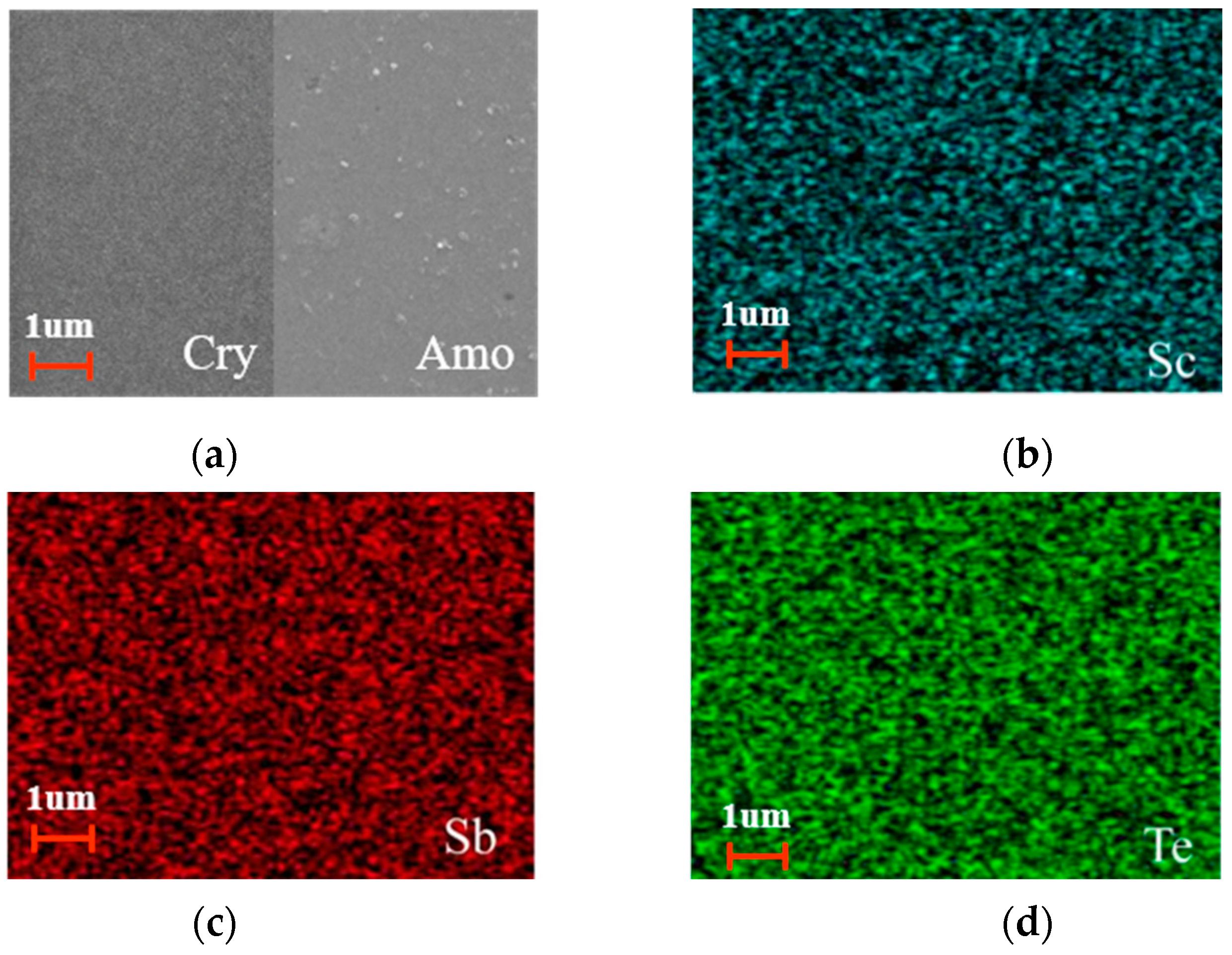
To verify the quality and performance of the SST films, the results of SEM and responding EDS maps of SST films are shown in
Figure 1. The surface elemental distribution of the deposited state film was relatively uniform and flat without obvious fluctuation. The surface elemental distribution of the deposited state film was relatively uniform and flat without obvious fluctuation. After annealing at 300 °C, the amorphous film transformed into a crystalline film, and uniform and dense grains appeared on the surface of the samples. According to the related reports on Sb
2Te
3 [
28,
29] and Bi-Sb-Te [
30,
31], this material as an abundant sb deposit had no significant effect on the atomic composition of the film. The average grain size was less than 20 nm, and the EDS spectrum image presented in
Figure 1 demonstrates the homogeneous elemental distribution with no impurities detected, demonstrating the excellent surface quality of the prepared deposited state films. We used the transfer matrix method to calculate the reflectance of different structure with the consideration of the amorphous and crystalline states of SST.
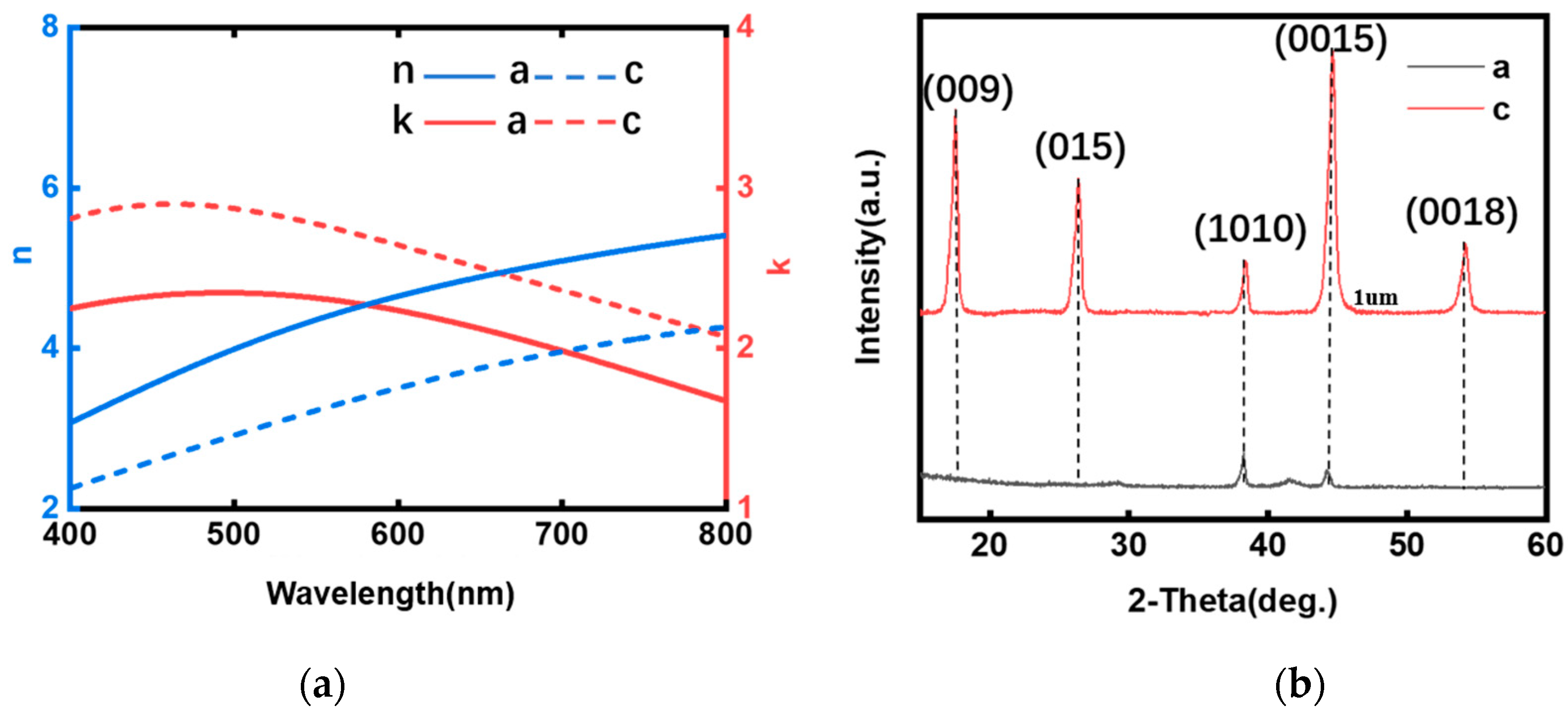
Figure 2a shows the distribution of refractive index n and extinction coefficient k of SST at wavelengths from 400 nm to 800 nm. There are significant differences in the refractive index (Δn = 1) and extinction factor (Δk = 1) between them. A feature enables smaller losses in SST applications and structure display, making the structure with better transmission efficiency, for the measurement of the n/k value, which has important application value for color device. Other optical material parameters are shown in
Table 1. As the annealing temperature increased, peaks appeared.
Figure 2b shows the XRD spectra of phase change material SST in amorphous (a) and crystalline (c) states. The XRD peaks of (009) and (015) were observed in the films, indicating that the crystallinity was improved while the average crystal grain size was increased. After high temperature, there will be an isomeric transformation, forming a dense hexagonal structure, which can achieve the transformation from amorphous to crystalline by annealing.
The color perception of the human eye caused by different wavelengths of visible light is different in the range of the visible light spectrum in order to unify the quantitative measurement of object color. In order to unify the quantitative measurement of object color, in 1931, the International Illumination on Commission (CIE) specified a set of standard chromaticity systems as CIE standard chromaticity systems: all color stimuli can be formed by the superposition of three specific polaritons. The three polaritons that match to form the color stimulus are called tristimulus values. The standard light source D65 is used here. The CIE1931 trisumulatory value with spectral transmittance under the light source with relative spectral power is calculated as:
where
, and it is a normalizing factor, S(
) is the relative spectral energy distribution of an illuminant,
is the relative spectral energy distribution of an illuminant,
is used to describe the lightness or luminosity of color, and
are used to determine color chromaticity.
A two-dimensional chromaticity was created by CIE to display different stimulus colors. The point (
,
) on CIE1931 represents the tristimulus value with the described color. By normalizing the tristimulus values, one of the components can be eliminated to form the color coordinates
and
:
3. Results and Discussion
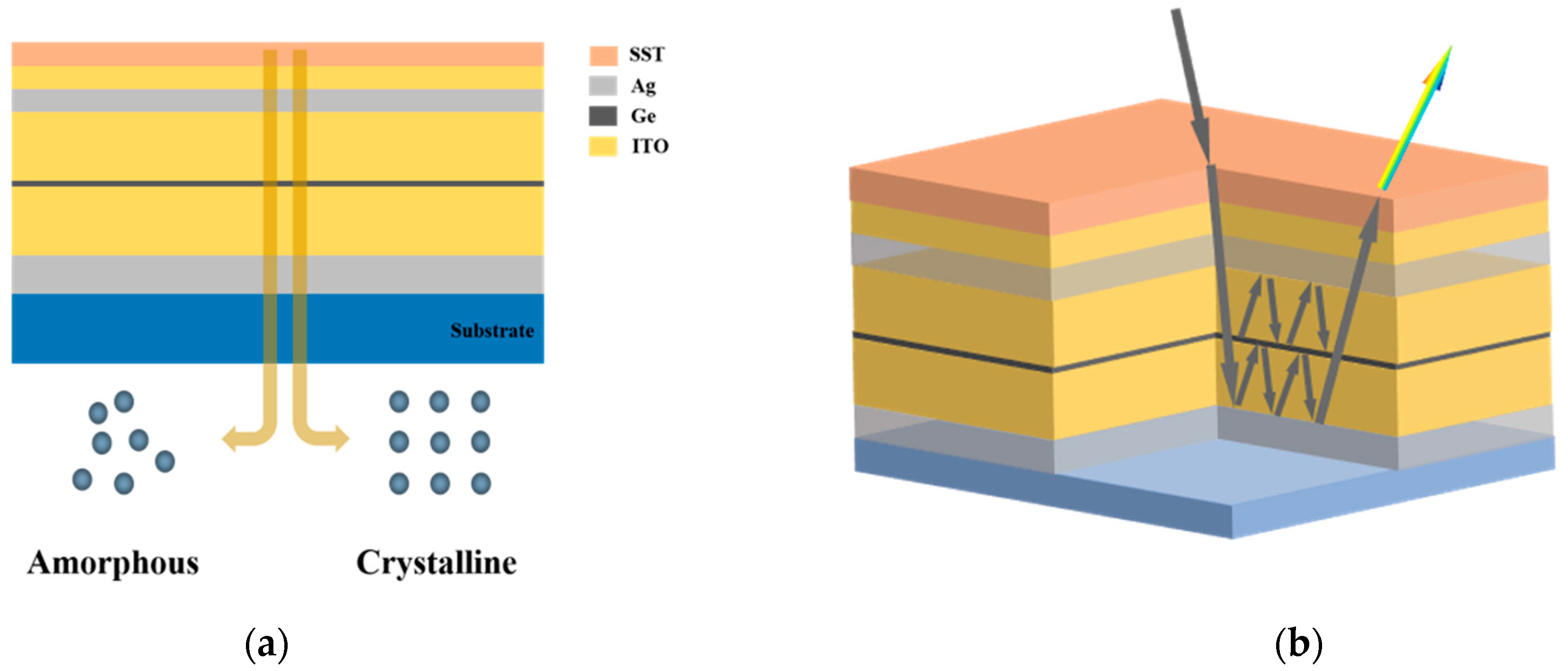
The schematic diagram of the multi-order F–P resonator structure is shown in
Figure 3a. The structure is composed of a 10 nm thick (H1) SST cover layer, 20 nm thick (H2) ITO, 18 nm thick (H3) AG, x nm thick (H4) ITO, 6 nm thick (H5) Ge, x nm thick (H6) ITO and 50 nm thick (H7) Ag stacked vertically from top to bottom to selectively form light wave resonance at specific wavelengths in the cavity. Under the stimulation of light, electricity, and heat, SST rapidly converts two types of solid state (crystalline state and amorphous state), and this conversion is reversible. The intermediate cavity layer was designed as an ITO dielectric layer with multi-order F–P resonance. The dielectric layer of ITO was incorporated in the middle by a highly reflective mirror overlaying the phase-compensated dielectric. ITO has a very high refractive index and negligible absorption index in the visible range, which can suppress the multi-order resonance wavelength, resulting in bright saturated color. Ag was used as a metal reflection layer because it has extremely low absorptivity and very high reflectivity in the visible light region, which can increase the peak of the reflection spectrum to 90%. Ge serves to separate the multi-order resonant cavities. The principle of light wave resonance is shown in
Figure 3b. The light forms a double-layer resonator in the MIMIP structure, which will result in a narrower width of the reflection peak and better structural monochromaticity. Furthermore, the increase in the number of resonators of the structure will cause the second harmonic of the structure in the visible light band, which greatly increases the monochromatic performance.
This is in contrast to previous studies where they used one of two factors, fwhm or reflectivity/transmissivity, to adjust saturation. In contrast, the multi-order F–P cavity resonance structure proposed in this paper balanced the two factors and also showed a high saturation, as shown in
Table 2. In the previously reported structures, the hue and saturation were commonly adjusted by the position of the absorber layer. In practical applications, it is first necessary to obtain definite position information and, more importantly, the hue and saturation are fixed after fabrication. We used the SST material, which can control the hue via the phase change between the crystal and amorphous states of SST. Since the structural color only involves the deposition method, it can be easily manufactured on a large area. The non-volatile color device can maintain the image without energy consumption, which is more energy-efficient.
To demonstrate the important properties of the top layer SST, we simulated the structure without the SST overlay. The reflection spectrum simulation results are shown in
Figure 4. In the absence of the top SST overlay, the visible light directly irradiates into the Ag layer, forming a highly reflective notch structure that creates a resonance wavelength bandwidth of about 100 nm. The additional phase change material SST will inhibit the highly reflective structure and greatly reduce the bandwidth. Therefore, we introduced an absorption medium (SST) into the cavity to form a multi-order resonant cavity to suppress the non-resonant wavelengths. At the same time, the amorphous and crystalline phases of phase change material SST can change the depth of color saturation. The bandwidth of the reflection spectrum was about 25 nm, and the peak of the reflection spectrum reached 90%. The amorphous state of the phase change material can keep the reflection wavelength of the non-resonant wavelength below 0.5%, while the crystalline state of the phase change material can keep the reflection wavelength of the non-resonant wavelength around 1.5%, which makes it possible to control the color depth through the two forms of the phase change material.
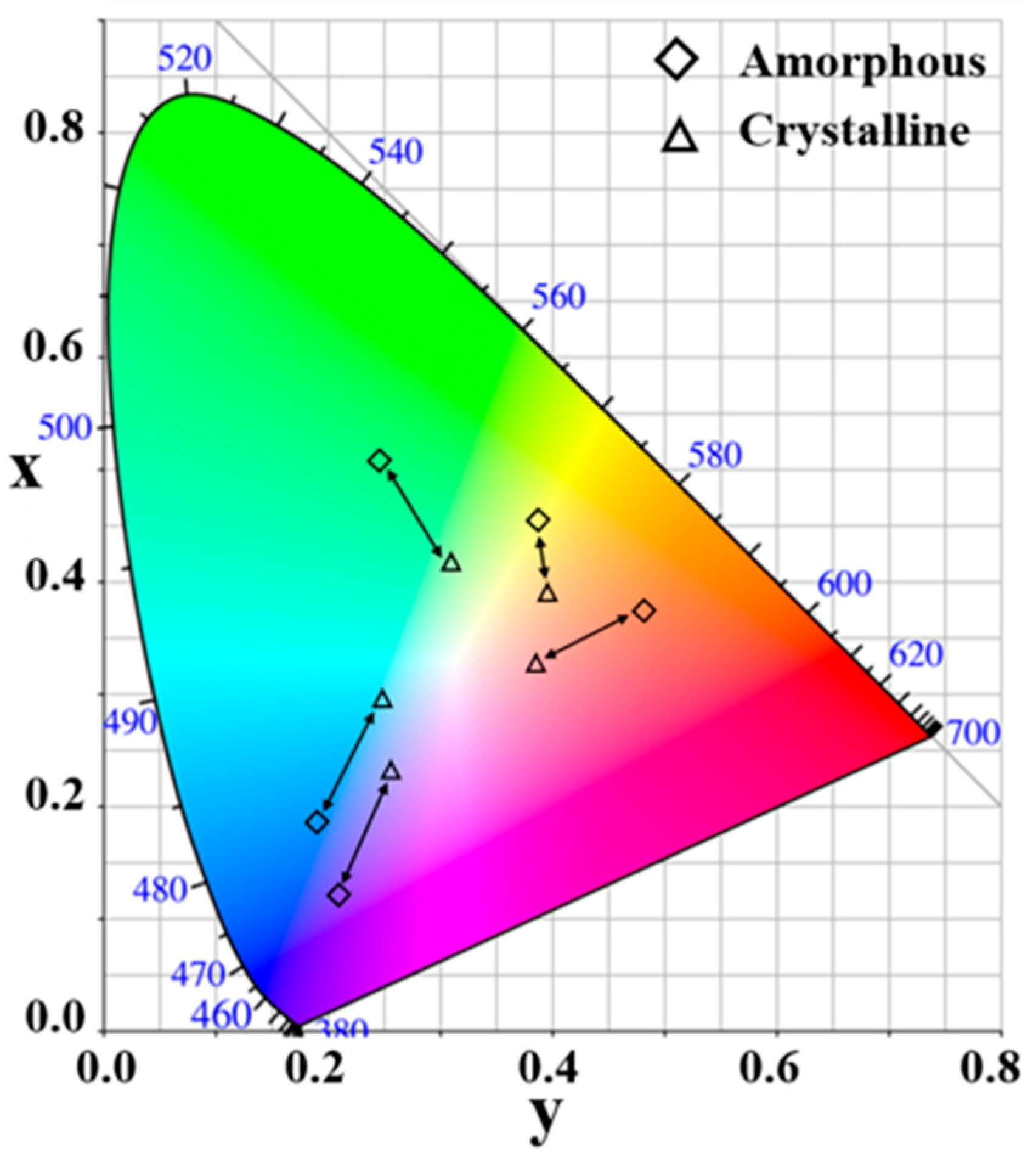
The diffraction space calculated from the simulated reflectance spectral curve was displayed on the CIE1931 chromaticity diagram to evaluate the color transition between the amorphous and crystalline states of the structure, as shown in
Figure 5, where the color space obtained from the reflection spectrum represented by the amorphous black squares is interconverted with the crystalline triangle: purple (0.2138, 0.1229) and light purple (0.2441, 0.2305), blue (0.2005, 0.1440) and light blue (0.2452, 0.2526), green (0.2264, 0.4722) and light green (0.3120, 0.4397), yellow (0.3849, 0.4489) interconverts with light orange (0.399, 0.3895), and red (0.4728, 0.3791) interconverts with light red (0.4003, 0.3256). This means that, with the MIMIP structure, changes in the color purity of the structure can be controlled by optical, electrical, and thermal means to achieve a wider color gamut.
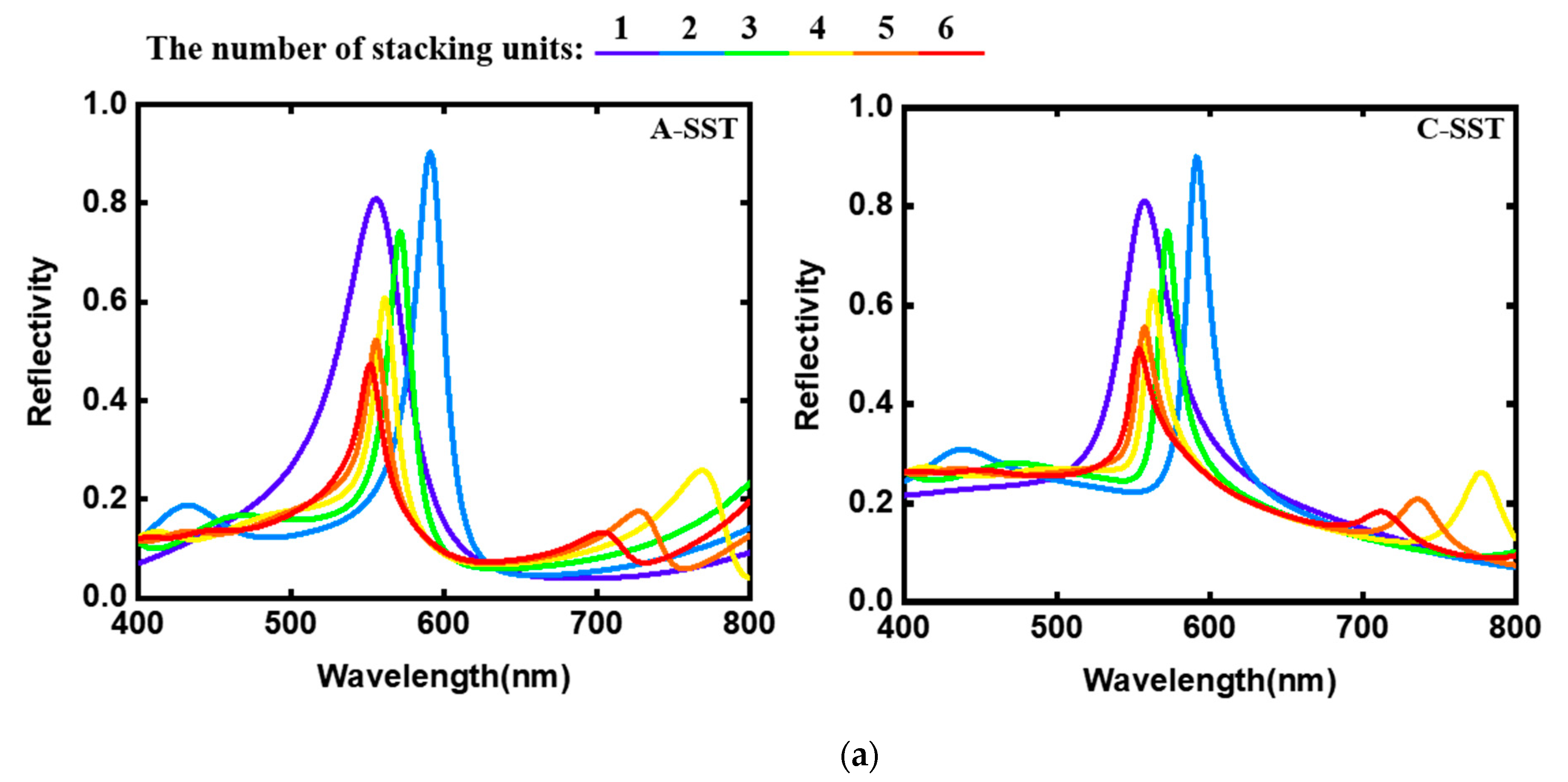
The disadvantage of the common F–P structure was that the FWHM of the reflection peak was relatively large, resulting in poor monochromaticity and dark color of the spectrum. To evaluate the effect of the F–P structure under different stacking units, we simulated the reflection spectra under different stacking units, as shown in
Figure 6a. The thicknesses of Ge and ITO layers in the stacking units are 6 and 130 nm. The FWHM of the reflection peak narrows with the increase in the number of stacked units. The peak value of the reflection peak is the highest in two unit cavities. As the number of stacked cells increases, the reflection spectrum gradually evolves from a flat curve to a curve with a smaller fwhm. This proves that the superposition of interference units can reduce the width of the reflection peak. With the increase in the number of stacking units, the peak value of the reflection peak reaches the peak of the two stacking units. Subsequently, the peak value of the reflection peak gradually decreases.
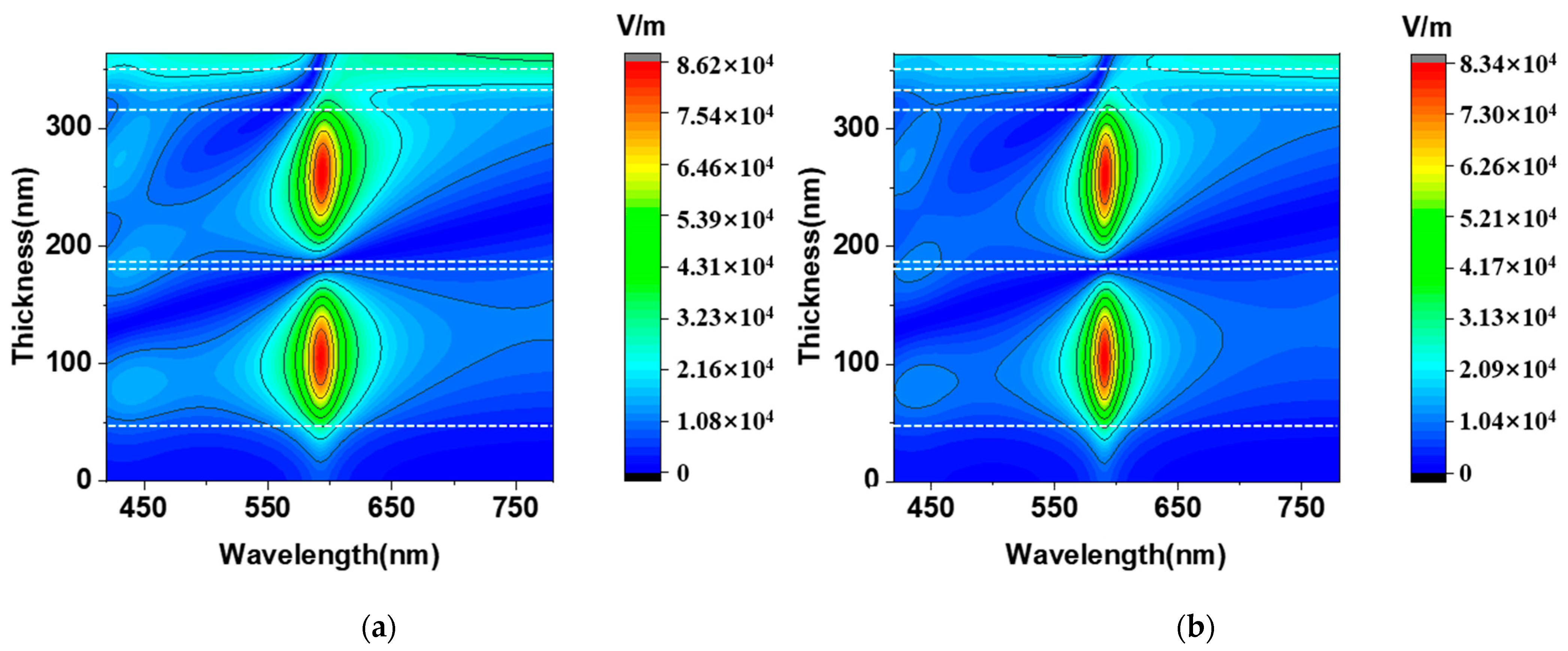
At the resonance wavelength of the structure, the electric field intensity changes along the depth of different stacking numbers, as shown in
Figure 6b. Some peaks of the electric field intensity profile appear in the ITO layer, showing strong resonance. As the stacking number increases, the electric field intensity peaks at the stacking of two stacking units, which indicates that the resonance intensity reaches saturation at a certain stacking. In addition, the maximum electric field intensity of the stack was obtained at the outermost ITO layer of the stack layer, and the lower ITO layer in the stack will gradually decline, but the ITO layer at the lowest end of the stack will rise to a certain extent. The bottom Ag layer causes the light field in the lowest layer to accumulate to some extent, which is clearly shown in the contour plot of the electric field intensity. Therefore, we chose a two-layer structure, which is more practical for color devices.
Here, we model the system using COMSOL to obtain the internal electrical field at visible wavelengths.
Figure 7 shows the electric field distribution of amorphous and crystalline structures of 50 nm Ag/130 nm ITO/6 nm Ge/130 nm ITO/18 nm Ag/20 nm ITO/10 nm SST. We obtain the distribution of the electric field intensity (|E|
2) for the above structure illuminated. The electric-field energy was mainly confined in the ITO layer, which demonstrates that the color filtering performance is caused by the F–P resonance effect. The phase change layer alters the resonance in the cavity through the phase shift and absorption changes. The absorption intensity of the crystalline state is higher than that of the amorphous state, which leads to a higher electric field peak in the amorphous state than that of the crystalline state. This results in chromatic differences between the structures in the amorphous and crystalline states.
In order to further study the performance of dynamic switching of structural color in the experiment, we quantitatively compared the thickness increase period of ITO in the amorphous and crystalline state of SST with COMSOL. We systematically simulated the reflectivity variations for different ITO thicknesses (ranging from 10 to 360 nm). The variation of reflectivity with different ITO thicknesses is shown in
Figure 8. When the ITO thickness is low (less than ~80 nm), the reflectivity is relatively flat, and no reflection peak is formed, which indicates that there is no resonance effect in the thin interferometer. As the ITO thickness gradually increases above 80 nm, the reflection peak has an obvious red shift at the peak position, as indicated by the black dashed lines in
Figure 8a. When the thickness of ITO increases above 160 nm, a secondary peak vibration occurs and multiple peaks appear, and the peak shifts of the reflection peaks of the amorphous and crystalline structures are basically the same, as shown in
Figure 8b. The reflectivity of the crystalline structure in the non-resonant band is lower than that of the amorphous structure. The non-resonant wavelength vibration of the amorphous state is close to 0%, while the non-resonant wavelength vibration of the crystalline state is close to 15%, which leads to a purer color of the amorphous state than the crystalline state. The color saturation can be adjusted by different forms of phase change materials.
Since the wavelength interference and absorption intensity of the multilayer structure depend on the thickness of the medium in the cavity, we changed the thickness of the two spacer layers x and H2. By fixing the thickness of Ag and phase change material SST, we obtained the palette for the entire visible light range. The comparison of the amorphous and crystalline color array palettes is shown in
Figure 9a. For the amorphous and crystalline palettes of SST, we adjusted the thickness of the upper ITO (H2) and the lower ITO (x), increasing the thickness of the upper ITO (H2) from 10 nm to 50 nm and the thickness of the lower ITO (x) from 50 nm to 180 nm. The color change in the color gamut diagram is a cycle from blue to red to blue again. In addition, after the cavity is fixed, the reflected color can be dynamically changed from dark to light by the dynamic modulation of the phase change material SST. When the phase change material SST changes from amorphous to crystalline, the interaction between light and matter and optical loss will increase. Thus, the dynamic control of color depth can be realized.
The comparison of amorphous and crystalline in different dielectric layers in simulation and experiment is shown in
Figure 9b. As the cavity length increases from 95 nm to 135 nm, the color gradually changes from green to red, and a clear red shift can be observed. The cavity length of the experimental sample was chosen in the interval of 5 nm so that the agreement with the simulated results could be better verified. The cavity length of the experimental sample was selected from the interval of 5 nm, which can better verify the consistency of the experimental and simulation results. The slight difference between the experimental sample and the simulated sample may be caused by the following two aspects: The light source used in the simulation is the standard D65 light source, and the experimental photos are taken under natural light; The simulation results are accurate to the nanometer level, and there may be a slight difference in film thickness between the experiment and simulation. Previously reported studies have shown that structures with wide fwhm or low reflectance/transmittance, red, green, and blue bands in the visible spectrum are selectively absorbed by resonant absorbers, producing sharp cyan, magenta, and yellow pixels. Our structure reflects a narrower FWHM with higher color saturation. The color of the sample is consistent with the wavelength of the reflection peak. The experimental results show that the hue and saturation can be adjusted easily in the proposed structure.
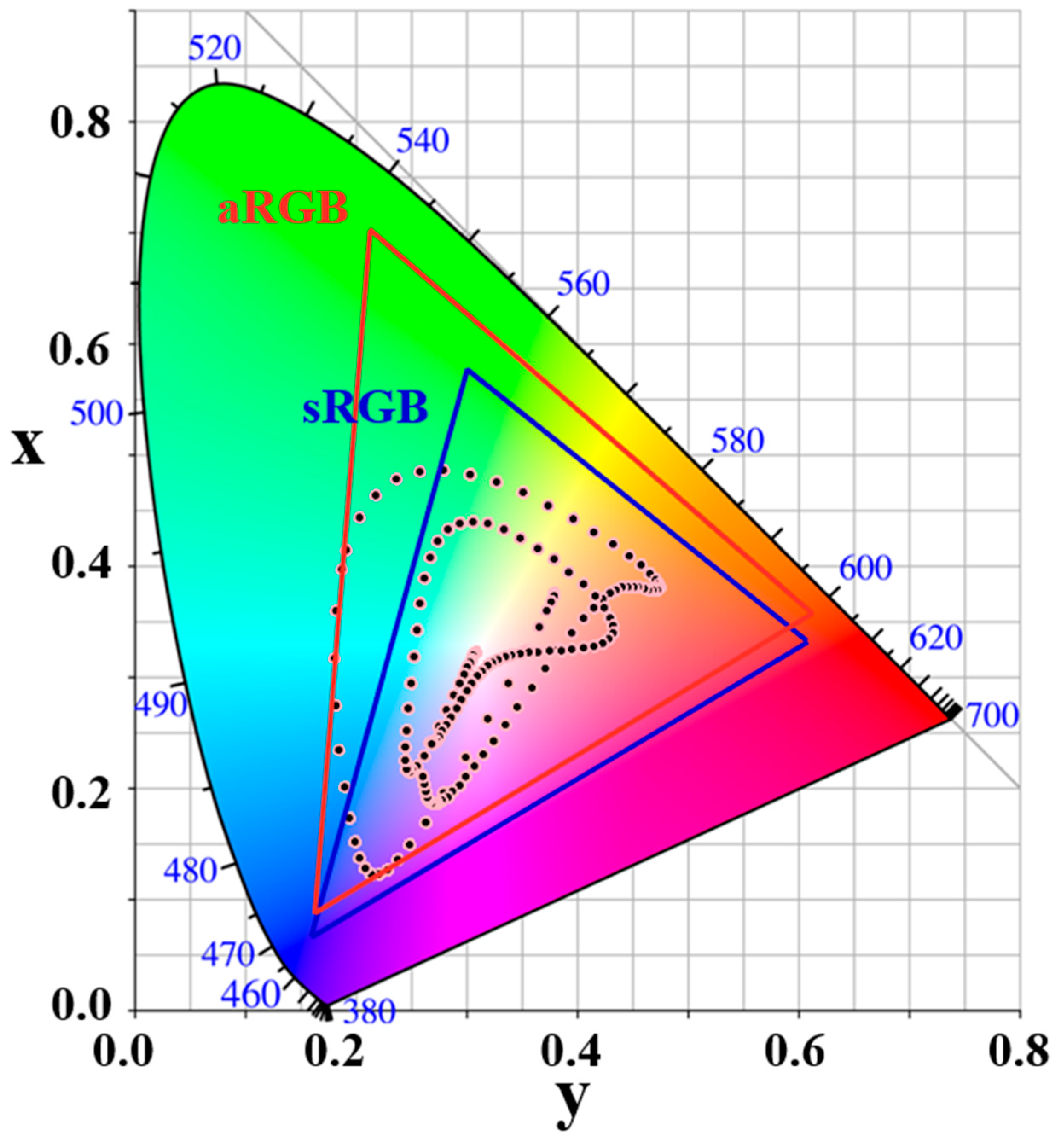
The colors (x, y) calculated from the reflection spectra of amorphous and crystalline states are displayed on the CIE1931 chromaticity diagram, as shown in
Figure 10. The spectra with high monochromaticity can produce purer colors. These colors are far away from the white point of the midline (0% saturation) and are closer to the color of the spatial contour of CIE1931. The simulated reflection spectrum of the structure accounts for about 60% of sRGB (the blue triangle in
Figure 10 is the area occupied by sRGB in the CIE1931 chromaticity diagram) and 50% of aRGB (the red triangle in
Figure 10 is the area occupied by aRGB in CIE1931 chromaticity diagram), which can prove that the structure can significantly increase the color gamut space and color saturation to meet the requirements of some basic color sensors.
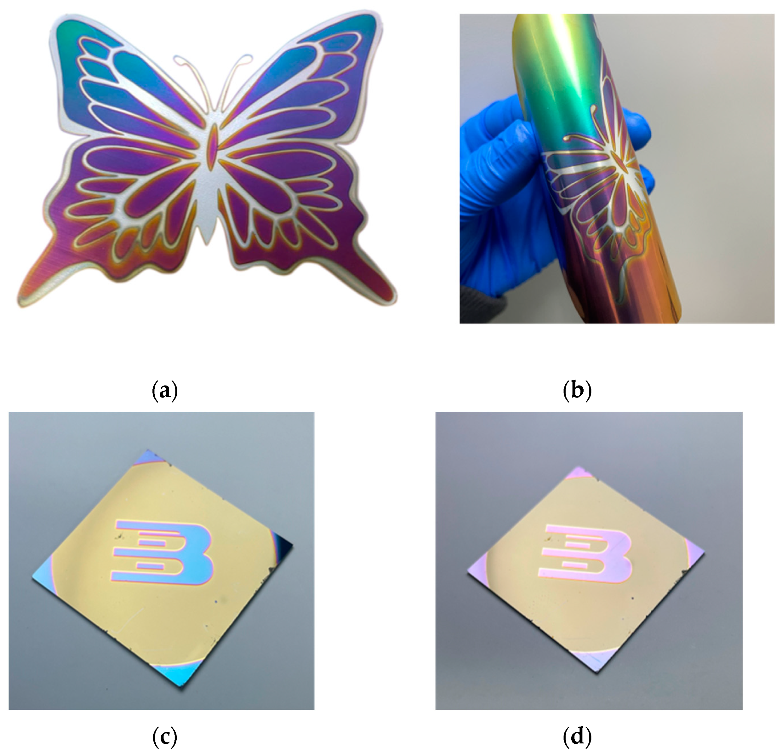
The color display is fabricated on a polyethylene terephthalate (PET) substrate, and the flexible color display is shown in
Figure 11a, a butterfly image was prepared via a mask process and magnetron sputtering. The color in the image is determined by different deposition thicknesses. The entire image is covered by a structure with an ITO of 90–170 nm, thereby presenting a colorful effect. The reflection optical properties of the structure are not sensitive to the bending radius, as shown in
Figure 11b. The structure described in this work could offer great potential for flexible wearable displays. The display effect of structures with amorphous and crystalline SST coating on Si substrate is shown in
Figure 11c,d, respectively (The pattern is the mark of the author’s alma mater). The blue color turns into a lavender color as seen from the transition from amorphous to crystalline after thermal annealing. The fabrication of this structure involves only membrane deposition, which can easily be fabricated on flexible substrates for color devices.
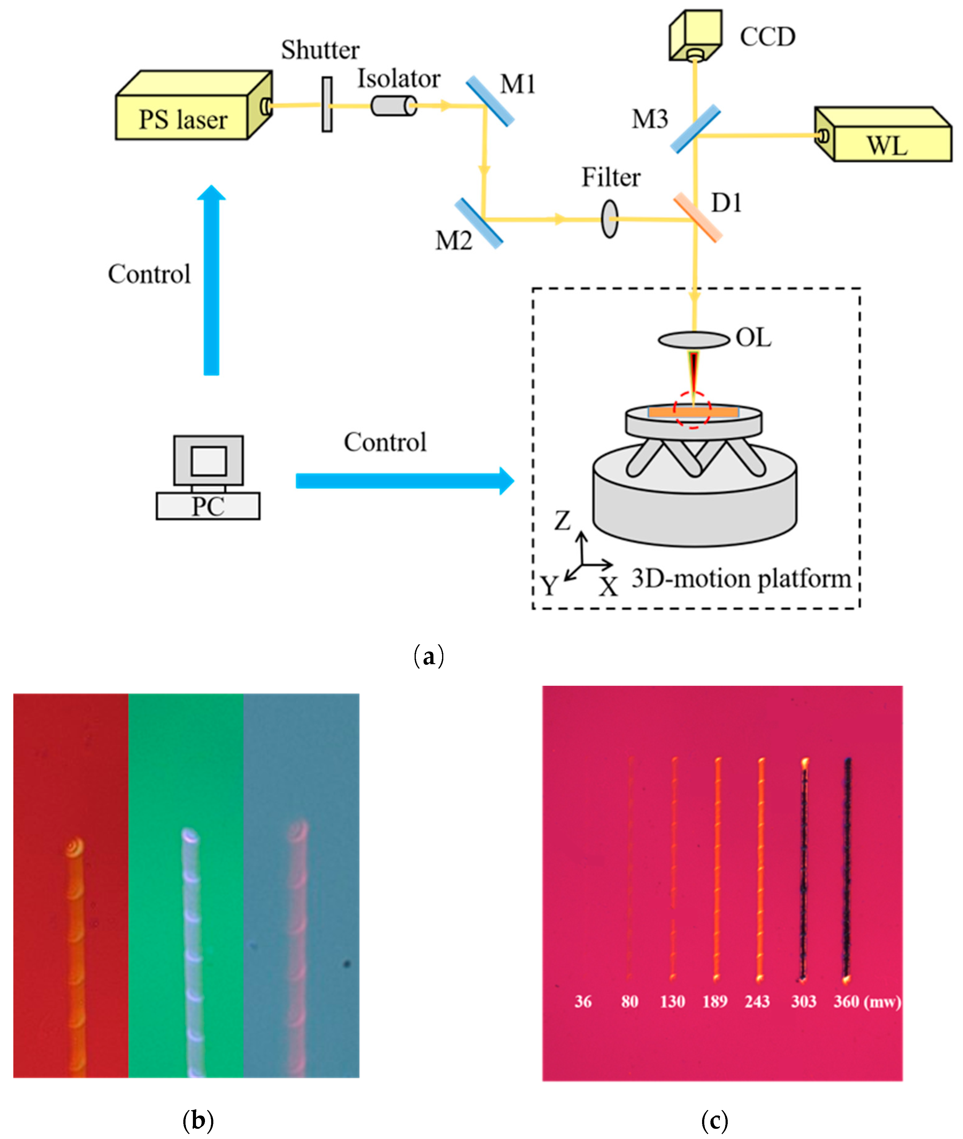
Laser-based printing techniques have been considered the most versatile due to their technical advantages such as rapid formation and the ability to manufacture almost any complex structure. In this study, the phase change of the SST layer was induced by picosecond laser pulses. The light path is shown in
Figure 12a. The sample was placed on a high-precision six-dimensional translation platform, and scanning lines were obtained by moving the platform during laser radiance. Here, three primary colors (RGB) were chosen as the substrate colors. The color of the base plate is shown in
Figure 12b, and after laser scanning, the red substrate changes to light red, the green substrate changes to light blue, the blue substrate changes to light pink, and the color changes from dark to light. The structure crystallization degree is different for a different power, and the color change after crystallization can also be controlled by controlling different laser power in
Figure 12c. It demonstrates that the structure can induce color change by laser, and the dynamic regulation of imaging equipment can be realized by laser. We demonstrate another capability of inexpensive large-area color pattern fabrication. The laser direct writing technology was used to induce structural discoloration, which can be used for very promising applications, such as imaging, anti-counterfeiting, and active optical devices.
