Abstract
The selectivity of the reactive ion etching of silicon using a negative electron resist AR-N 7520 mask was investigated. The selectivity dependencies on the fraction of SF6 in the feeding gas and bias voltage were obtained. To understand the kinetics of passivation film formation and etching, the type and concentration of neutral particles were evaluated and identified using plasma optical emission spectroscopy. Electron temperature and electron density were measured by the Langmuir probe method to interpret the optical emission spectroscopy data. A high etching selectivity of 8.0 ± 1.8 was obtained for the etching process. The optimum electron beam exposure dose for defining the mask was 8200 pC/m at 30 keV.
1. Introduction
Electron beam lithography (EBL) is used in different research fields for prototyping [1] due to its high resolution [2]. The EBL resolution is defined by the properties of e-beam resist and by processes during development and exposure [3,4,5,6,7]. Therefore, the study of the e-beam resist properties, optimization of the EBL parameters, and the etching process are important for nanoelectronics and photonics.
In particular, e-beam resist is used to fabricate photonic structures such as waveguides and diffraction gratings [8,9,10,11,12]. For example, the high resolution and plasma etching resistance of hydrogen silsesquioxane (HSQ) enable the fabrication of structures with vertical sidewalls, low sidewall roughness, and a desirable aspect ratio [13,14]. However, the removal of the HSQ resist requires a wet etch process using hydrofluoric acid HF, which complicates the formation of structures. The structures are often formed in silicon on SOI substrates. After development, the HSQ resist presents a structure close to SiO2. The removal of the resist in HF may damage the SiO2 layer. The removal of AR-N 7520 is carried out in oxygen plasma.
The negative e-beam resist AR-N 7520 is one of the novolaks (low-molecular-weight polymers derived from phenols and formaldehyde) and has very high contrast, excellent transfer of structures, and high-precision edges [15]. AR-N 7520 can be easily removed in acetone or oxygen plasma. Due to these characteristics, the AR-N 750 resist is suitable for the formation of photonic structures. The resist is used to form various structures, such as silicon nanopillars for photodetectors, nanosensors, optical interconnects, and microresonators [16,17]. AR-N 7520 has also been used to form nanofilaments with pn-junctions as elements of a nanoscale thermal time of flight (TToF) sensor [17].
Sidewall roughness is an important parameter for the correct work of photonic structures. The high roughness of waveguide sidewalls leads to power losses in waveguides, as well as errors associated with the backscattering effect [18]. The sidewall roughness of the line pattern obtained by EBL is transferred to the structures during reactive ion etching (RIE). Thus, an important task for the production of high-quality structures is to obtain a resist mask with minimal sidewall roughness.
It is well known [19] that the slope angles of the sidewalls of the obtained structures depend on the feeding gas composition. Different tasks of photonic require structures with different sidewall slopes. It is important to study the influence of the feeding gas composition on the sidewall slope angle.
The problem of determining the resist plasma etching resistance and etching selectivity of materials (the ratio of their etching rates) becomes more relevant if the obtained results can be compared with the data obtained in tools of other designs or processes with other technological parameters. For this purpose, the character and concentration of neutral particles in the investigated range of the feeding gas compositions were evaluated and identified using plasma optical emission spectroscopy and actinometry. The electron temperature and electron density were measured using the Langmuir probe method to interpret the optical emission spectroscopy data.
The study of EBL and RIE processes with AR-N 7520 could enable a technology for forming silicon waveguides and other photonic nanostructures with lower sidewall roughness and different aspect ratios.
2. Materials and Methods
The p-type silicon (100) wafers were pretreated in n-methylpyrrolidone and acetone. Then, the wafers were annealed at 150 °C for 30 min in a N2 ambient atmosphere for dehydration. To promote adhesion, the silicon wafer was held in hexamethyldisilazane (HMDS) vapor at 85 °C for 10 min. The AR-N7520 with a concentration of 7.3% (PGMEA, 1-methoxy-2-propanol acetate) was spin-coated onto the surface using an SM-180 centrifuge (SAWATEC AG, Switzerland, Sennwald) at a centrifuge speed of 3000 rpm. The wafers were annealed at 85 °C for 5 min in N2 ambience. The thickness of the resist layer was measured using a spectral ellipsometer M-2000X (J.A. Woollam Co., Inc., Lincoln, NE, USA) [20,21] and amounted to 100 ± 1 nm.
The exposure was carried out using the EBL system Raith-150 (Raith, Dortmund, Germany). The electron beam energy was 30 keV, and the beam current was 150 pA. The step size value was 6 nm. Pattern of lines of 1 mm in length were formed. Single lines were chosen as the test object to avoid the influence of the proximity effect. Information for the line group in the RIE process is similar, taking into account the change in dose for the proximity effect. The line exposure dose ranged from 4000 to 16,000 pC/cm with a step of 200 pC/cm. The wide range of doses was chosen to find the optimal dose to obtain structures with low sidewall roughness and the required aspect ratio.
Development was performed in the developer AR 300-47 for 50 s at 21 °C. Then, the wafers were treated in deionized water for 30 s, isopropanol for 20 s, and in a flow of dry nitrogen. After development, wafers were annealed at 85 °C for 3 min in a N2 ambient.
An anisotropic RIE was performed to investigate the plasma resistance of AR-N 7520 and the selectivity of the silicon etching. RIE was performed on a Dual PlasmaLab 100 (Oxford Instruments Plasma Technology, Bristol, UK) using inductively coupled plasma (ICP) of the SF6/C4F8 feeding gas excited at 2 MHz. The cylindrical process chamber was 450 mm high and 380 mm in diameter. A DC bias on the sample was created by a 13.56 MHz RF generator powered by 18–47 W, providing an equivalent constant bias voltage VDC in the range of −80–150 V. The wafers were segmented to obtain a set of 2 × 2 cm coupons with identical patterns of lines. The coupons were glued on a 100 mm diameter silicon carrier wafer by PFPE grease and helium with a pressure of 7 Torr introduced under the carrier, ensuring the thermal contact of both the sample with the carrier and the carrier with the table in the chamber. Helium flow below the carrier to the process chamber was about 4 sccm, and the partial pressure of He in the process chamber can be estimated as 0.5 mTorr according to the ratio of flows. The reactor table was thermally stabilized at a temperature of 20 °C. The optical port for plasma diagnostics was 10 cm above the table. The base pressure in the reactor chamber was 10−6 Torr. The chamber pressure during the etching process was 10 mTorr, the total gas flow was 70 sccm, and the ICP power was 1200 W. The gas residence time was 0.57 s, and the mean energy input per one molecule in the chamber was 595 eV/molecule.
The influence of the SF6 fraction in feeding gas in the range of 15–35% was investigated at −125 V DC bias. The effect of DC bias voltage on the etching process was studied in the range of −80 V–150 V at a constant fraction of SF6 in feeding gas at 22%. The etching process time was 30 s. It was the same for all the samples. The selectivity of the silicon RIE through the AR-N7520 mask was calculated as the ratio of the Si etching depth to the decrease in the height resist line during the etching process:
where dSi is the depth of silicon etching, d0 is the height of the resist line before etching, and d is the height of the resist line after etching.
Probe characteristic measurements were performed using a single Langmuir probe Espion (Hiden Analytical, Warrington, UK). The probe was made of tungsten wire with a diameter of 0.15 mm and a length of 10 mm. The probe electrode was installed through a port on the sidewall of the chamber. During the measurements, the probe potential was varied from −100 V to +20 V in steps of 0.05 V. To minimize the errors induced by the deposition of fluorocarbon polymer on the probe surface, the probe was subjected to pre-cleaning by ion bombardment in 50% Ar + 50% O2 plasma. Our previous studies [22] demonstrated the efficiency of such a procedure for polymerizing plasma.
The absolute value of the concentration of neutral atomic particles was estimated using the spectrometric method of optical emission actinometry. For this purpose, the emission spectra of SF6/C4F8 plasma with a small addition of Ar (6%) were measured [18].
Concentrations of molecular fluorocarbon species were estimated from the emission intensity of these particles using optical emission spectroscopy. The emission spectra were measured using an HR4Pro spectrometer (Ocean Insight, Orlando, FL, USA) in the wavelength range 200–900 nm with an optical resolution of 0.7 nm.
Images of the pattern of lines after etching and the thickness of the AR-N 7520 resist before and after the etching process were obtained using a scanning electron microscope (SEM) Ultra 55 (Carl Zeiss AG, Jena, Germany).
3. Results
3.1. Exposure Dose
The study of the samples after development was carried out to determine the dependence of the line height on the exposure dose. Figure 1a–c show SEM images of structures with different line exposure doses. The dependence of the line height on the exposure dose is presented in Figure 1d. It can be seen from the graph that the optimal value of the line exposure dose is 8200 pC/cm. Larger doses require a longer exposure process at almost the same exposure efficiency.
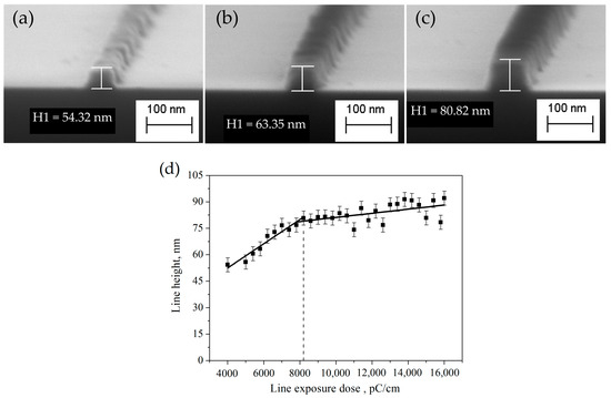
Figure 1.
(a–c) SEM images of samples after development. Lines with exposure doses of (a) 4000 pC/cm, (b) 5800 pC/cm, and (c) 8200 pC/cm are presented. (d) Dependence of line height after development on the line exposure dose.
With the increasing exposure dose, higher absorbed energy leads to the breaking of molecular units [23]. The linear dependence of line roughness on the line exposure dose is shown. Line roughness decreases with an increasing exposure dose. The dependence allows us to choose the optimal line exposure dose considering the line height, LER, and time of line exposure.
A study of the dependence of line edge roughness (LER) on the exposure dose was also carried out (Figure 2).
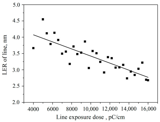
Figure 2.
Dependence of line edge roughness (LER) on exposure dose.
3.2. Passivation and Etching Kinetics
Understanding the kinetics of passivation and etching allows for more effective control of the RIE process by varying the SF6 fraction in the SF6/C4F8 mixture. The decomposition kinetics of C4F8 molecules and the products formed in the ICP discharge of such gasses have been well studied [24]. To understand the deposition and etching kinetics, the most interesting neutral particles can be identified using plasma optical emission spectroscopy. The fluorine atom is responsible for the etching process in the presence of ion bombardment, and CF and CF2 are the particles involved in the formation of the fluorocarbon film [25,26,27].
Measurements of plasma characteristics by the Langmuir probe method have been carried out in the investigated range of plasma feeding gas composition. It is shown that the electron density is 1.0 × 10¹⁰–1.2 × 1010 cm−3 with the varying SF6 fraction from 15% to 35% and depends weakly on the plasma composition. The linear dependence of the logarithm of the electron current on the probe voltage shows that the electron energy distribution function (EEDF) is Maxwellian with high accuracy [22], and the electron temperature (Te) is in the range of 2.3–2.6 eV. One can estimate the actinometric coefficient for the Ar and F line pair, which varies weakly in this range of Te values [28]: = 4.68 ± 0.03. According to [28], the population of the excited state of the F and Ar lines (685.6 nm and 750.4 nm, respectively) is produced by direct electron impact under similar conditions. Due to the low pressure (10 mTorr), the time between collisions, in our case, is much longer than the radiation time of the mentioned transitions, so the quenching process can be neglected. This makes the correct actinometry of atomic fluorine in argon possible [29].
In the case of the actinometry of molecules, the situation is more complicated since there is a large difference in the electronic excitation threshold of CF2 and Ar (about 5 eV and 14 eV, respectively), and there are reports on the effective excitation of fluorocarbon radicals, such as CF and CF2, in collisions with the metastable particles of noble gasses [30] (in our case, He was present in the discharge and supplied to enable the cooling of the sample). However, in several works, such studies were performed [31] and verified by laser-induced fluorescence (LIF) [32,33].
Since the contributions of different kinds of fluorocarbon radicals of CFx species to the process of polymer formation on the surface remain experimentally unconfirmed, actinometric measurements become more complicated. In the present work, it was decided to use the intensity of the overlapped molecular band transitions CF2 A1B1(0;3;0)–X1A1(0;0;0) and A1B1(0;4;0)–X1A1(0;1;0) [31,32] (262.5 nm) to estimate the film-forming ability of the plasma.
The overview spectrum of the discharge at the SF6 fraction in the feeding gas was equal to 18% (Figure 3a), corresponding to the typically observed spectra in SF6/C4F8 plasma. Neutral atomic Ar, F, and C radicals were clearly observed in the spectra with wavelengths shown in Figure 3a. Molecular bands of the B2Δ-X2Π transition of the CF radical, CF2 (A1B1–X1A1), and so-called Swan band of the C2 molecule (d3Pg–a3Pu transition) were detected. The spectrum of molecular bands and the CFx continuum in the UV region for SF6/C4F8 plasma under experimental conditions is shown in Figure 3b. The overlap of CF2 (A1B1–X1A1) bands and the CF2+ continuum [34] can be observed for the wavelength range of 235–270 nm.
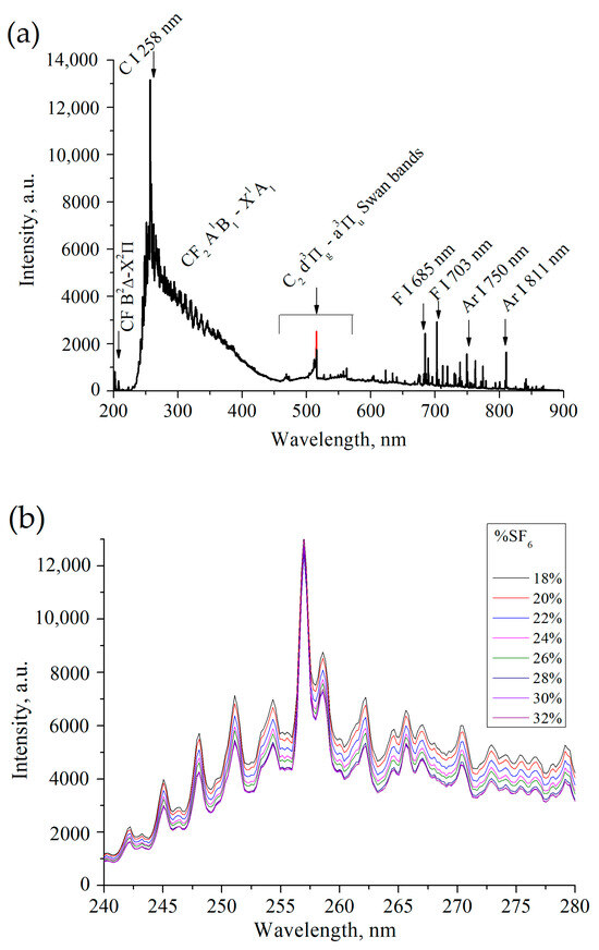
Figure 3.
(a) Plasma spectrum of the SF6/C4F8 feeding gas composition under experimental conditions with the SF6 fraction equal to 18%. The fraction of Ar is equal to 6%. (b) Spectrum of molecular bands and CFx continuum in the ultraviolet region for SF6/C4F8 plasma under experimental conditions.
Figure 4 shows the dependence of atomic fluorine concentration in the plasma composition with the increasing the SF6 fraction in feeding gas, and also the dependence of the intensity of the overlapped molecular bands CF2 A1B1(0;3;0)–X1A1(0;0;0) and A1B1(0;4;0)–X1A1(0;1;0) 262.5 nm on the SF6 fraction.
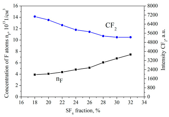
Figure 4.
Dependence of atomic fluorine concentration and intensity of the overlapped CF2 molecular bands A1B1(0;3;0)–X1A1(0;0;0) and A1B1(0;4;0)–X1A1(0;1;0) (262.5 nm) on the SF6 fraction in the feeding gas.
An increase in the fraction of SF6 leads to a monotonic increase in the fluorine concentration in the plasma composition and a decrease in the intensity of the CF2 molecular band. The fluorine radical concentration increases from 3.8 × 1013 cm−3 to 6.3 × 1013 cm−3 and the intensity of the CF2 molecular band decreases by 25% with an increase in the fraction of SF6 from 18% to 35%. Varying the plasma feeding gas composition, it is possible to change the passivation/etching balance on the surface, which can be used as a controlling knob for etching selectivity.
3.3. Control of the Etching Parameters
Etching selectivity can be controlled by monitoring the plasma composition, the kinetics of the surface reactions, including ion-stimulated reactions, and the condition of the treated surface. To optimize silicon RIE through the AR-N 7520, the mask influence of the SF6 fraction in the feeding gas (15%, 18%, 25%, 28%, 31%, and 35%) was studied.
Figure 5 shows the dependence of the silicon etching rate (RSi), resistetching rate (RAR-N), and selectivity (S) for the RIE at different SF6 fractions for the feeding gas and bias voltage VDC = −125 V.
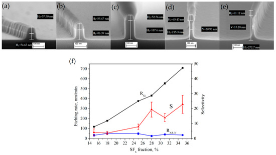
Figure 5.
(a–e) SEM images of samples after the process of RIE. Structures after processes with SF6 fractions of (a) 15%, (b) 18%, (c) 25%, (d) 28%, and (e) 31%. (f) Dependence of silicon-etching rate, the etching rate of AR-N 7520, and selectivity on the SF6 fraction in the feeding gas. The mean error values for the silicon and resistetching rates were 5.5 nm/min and 8.5 nm/min, respectively.
The concentration of fluorine atoms in the plasma composition increases with the increasing SF6 fraction. This can explain the increase in the etching rate of silicon. The kinetics of silicon etching by atomic fluorine in the unsaturated regime provides an almost linear dependence of the etching rate on fluorine concentration [29]. The etching rate of the AR-N 7520 resist depends on the concentration of atomic fluorineweakly. The etching rate of AR-N 7520 is determined by the rate of ion transport to the surface since ion bombardment is the main mechanism of its etching. Thus, the resistetching rate remains almost constant with an increasing fraction of SF6 in the feeding gas, and the etching selectivity of silicon to AR-N 7520 increases. The process with a fraction of SF6 in the feeding gas equal to 25% and a bias voltage of −125 V provides an etching selectivity of 8.0 ± 1.8.
The dependence of the material etching rates on the incident ion energy, which is usually the threshold in nature, can also play an important role in controlling etching selectivity. The sputtering rate has a square root dependent on energy, with different threshold energies for different materials. Choosing ion energies close to sputtering thresholds can lead to an increase in selectivity. By varying the bias voltage, it is possible to optimize the ratio of etching rates.
Figure 6 shows the dependence of the silicon-etching rate (RSi), resist etching rate (RAR-N), and selectivity (S) at the different values of bias voltage (−80 V, −100 V, −150 V) in the process of RIE and with a constant fraction of SF6 in the feeding gas equal to 22%.
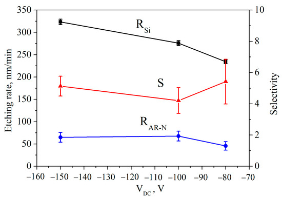
Figure 6.
Dependence of silicon-etching rate, the etching rate of AR-N 7520 resist, and selectivity on the bias voltage. The mean error values for the silicon- and resist etching rates were 5.2 nm/min and 10.5 nm/min, respectively.
With increasing bias voltage, the silicon-etching rate increased monotonically. The resist etching rate in the voltage range from 100 V to 150 V grew insignificantly. The process at a constant fraction of SF6 in the feeding gas equal to 22% allowed an etching selectivity of 5.0 ± 1.4 to be obtained.
The dependence of the etching selectivity on the exposure dose was investigated. The data were obtained for processes with different values of bias voltage (Figure 7).
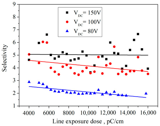
Figure 7.
Dependence of selectivity on the exposure dose for etching processes with different values of bias voltage.
Selectivity depends on the exposure dose weaklyfor processes with different values of bias voltage.
3.4. Sidewall Slope in the Process of RIE
The influence of the feeding gas composition on the sidewall angle of the silicon structure was also investigated. Figure 8 shows the dependence of the sidewall angle α on the SF6 fraction in the feeding gas during RIE.
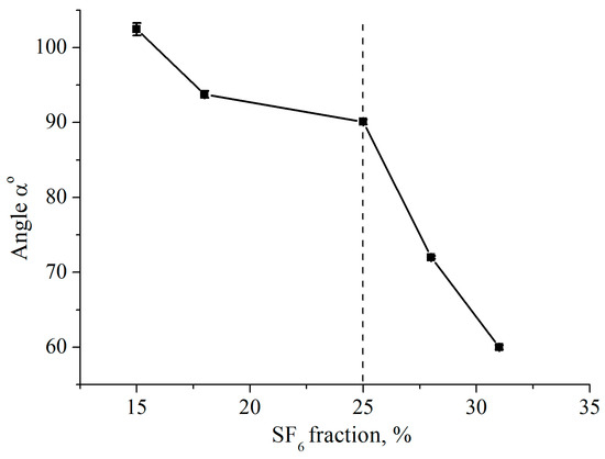
Figure 8.
Dependence of the silicon structure sidewall angle on the SF6 fraction in SF6/C4F8 feeding gas. SEM images of the structures are shown in Figure 5a–e.
A reduction in the sidewall slope with an increasing SF6 fraction is observed. CFx radicals in plasma are responsible for fluorocarbon film deposition on the surface [35], so, as shown in Figure 3, the increase in the SF6 fraction in plasma decreases the CFx concentration and, consequently, inhibits film deposition. Another reason for the decrease in the sidewall profile angle is the increase in the fluorine radical concentration since fluorine radicals can spontaneously etch silicon sidewalls. Varying the plasma deposition changes the ratio between the etching and passivation balance and controls the sidewall slope. Another effect observed in SF6/C4F8 plasma causing the sidewall profile slope is the charging of the bottom of the etched structures and deflection of positive ions [36]. However, this effect was observed for structures with a higher height and aspect ratio than for the structures presented in our work, and the plasma feeding gas composition was in a slightly different range of values. So, in our work, the sidewall slope was unlikely due to the charging of the bottom of the structures. Thus, by changing the ratio of the gas fraction in the feeding gas, it is possible to control the sidewall slope in the structure. Using the 25% fraction of SF6 in the SF6/C4F8 feeding gas allowed us to obtain structures with a sidewall slope angle of 90.1 ± 0.3°.
4. Discussion
The study of structures after development, obtained at various exposure doses (from 4000 pC/cm to 16,000 pC/cm), made it possible to determine the optimal value for the exposure dose to obtain structures with vertical walls and a sufficient aspect ratio. The different characteristics of the structures are explained by the sensitivity and contrast of the AR-N 7520 resist. The study of the dependence of selectivity on the exposure dose for etching processes with different parameters shows a weak dependence for all etching processes (Figure 7 and Figure S1). The structures obtained at an exposure dose of 8200 pC/cm are optimal in terms of aspect ratio, LER, and wall verticality for studying etching processes and the formation of photonic structures.
The change in the selectivity and etching profile angle is due to a change in the etching rate of silicon. The silicon-etching rate changes approximately two times when the SF6 proportion changes from 18% to 32%, while the fluorine radical concentration grows from 3.8 × 1013 cm−3 to 6.38 × 1013 cm−3. The dependence of the Si-etching rate on the DC bias is close to the root function, which indicates the contribution of ion stimulation to vertical etching. The etching rate of the resist does not depend on the plasma composition in the studied range, which corresponds to the ion-stimulated-etching regime limited by ion flux toward the surface. The etching rate of the resist is tens of nanometers per minute.
The trade-off between profile angle and selectivity is related to the balance between passivation and etching. This effect is explained by a change in the ratio of the concentration of CFx and F radicals. When etching vertical structures with a profile angle of 90, the selectivity of silicon to AR-N 7520 etching is eight, which is a sufficiently high value for creating structures of photodetectors, nanosensors, and microresonators [16,17]. At the same time, the production of cone silicon nanopillar arrays, when it is necessary to obtain structures with a profile angle not equal to 90°, is relevant for the manufacture of photovoltaic structures [16] and biomedical applications [37]. In addition, controlling the angle of the resulting structures is important when implementing the deep etching process when the effect of the aspect dependence of etching is significant.
5. Conclusions
The e-beam AR-N 7520 resist has excellent characteristics for fabricating photonic structures, but its interaction with fluorine plasma has not been widely studied. Our study shows that the resist has a high plasma resistance. The study of the plasma resistance of the AR-N 7520 was carried out. The selectivity of silicon RIE using a negative electron resist mask AR-N7520 was also obtained. The optimum electron beam exposure dose for defining the mask was found to be 8200 pC/m at 30 keV. Selectivity was weakly dependent on the exposure dose at dose values over 4000 pC/cm.
Plasma parameters were measured by the Langmuir probe for different feeding gas compositions. It is shown that the electron density was 1.0 × 10¹⁰–1.2 × 1010 cm−3 and depended weakly on the plasma composition. The EEDF is shown to be Maxwellian with high accuracy, and the electron temperature is in the range of 2.3–2.6 eV. Actinometry data show an increase in the concentration of atomic F when the SF6 fraction in the feeding gas is increased from 18% to 32%. On the other hand, the reduction in intensity of the molecular bands in the region of 250–400 nm indicates a decrease in the concentration of fluorocarbon components in the plasma that causes the deposition of polymers on the surface.
The dependence of the selectivity of silicon etching using a negative electron resist mask AR-N7520 at the SF6 fraction in the range of 15%–35% was obtained. The dependence on bias voltage in the range of 80 V–150 V was also studied. The process with an SF6 fraction of 25% and a bias voltage of 125 V provided an etching selectivity of 8.0 ± 1.8. The obtained selectivity was sufficient for small-volume production using e-beam lithography. The sidewall angle was 90.1 ± 0.3°. Thus, the e-beam AR-N 7520 resist is suitable for application in the formation of photonic structures.
Supplementary Materials
The following supporting information can be downloaded at https://www.mdpi.com/article/10.3390/pr12091941/s1. Figure S1: Dependence of selectivity on exposure dose for etching processes with different values of SF6 fraction.
Author Contributions
Conceptualization, K.F. and A.T.; methodology, A.T., A.R. and A.M. (Alexander Melnikov); validation, K.F. and V.K. (Vitaly Kuzmenko); formal analysis, K.F.; investigation, K.F., A.M. (Andrey Miakonkikh), O.G. and V.K. (Vsevolod Kiselevsky); resources, A.R. and A.M. (Alexander Melnikov); data curation, K.F.; writing—original draft preparation, K.F.; writing—review and editing, V.K. (Vitaly Kuzmenko), A.R., A.T. and A.M. (Andrey Miakonkikh); visualization, K.F. and V.K. (Vitaly Kuzmenko); supervision, A.T., A.R. and A.M (Alexander Melnikov).; project administration, A.T. and A.R.; funding acquisition, A.R. All authors have read and agreed to the published version of the manuscript.
Funding
The investigation was supported by Program no. FFNN-2022-0021 of the Ministry of Science and Higher Education of Russia for Valiev Institute of Physics and Technology of RAS.
Data Availability Statement
The dataset is available upon request to the authors.
Acknowledgments
The investigation was supported by Program no. FFNN-2022-0021 of the Ministry of Science and Higher Education of Russia for Valiev Institute of Physics and Technology of RAS.
Conflicts of Interest
The authors declare no conflicts of interest.
References
- Menon, R.; Patel, A.; Gil, D.; Smith, H.I. Maskless lithography. Mater. Today 2005, 8, 26–33. [Google Scholar] [CrossRef]
- Zeitner, U.D.; Oliva, M.; Fuchs, F.; Michaelis, D.; Benkenstein, T.; Harzendorf, T.; Kley, E.B. High-performance diffraction gratings made by e-beam lithography. Appl. Phys. A 2012, 109, 789–796. [Google Scholar] [CrossRef]
- Broers, A.N.; Hoole, A.C.F.; Ryan, J.M. Electron beam lithography—Resolution limits. Microelectron. Eng. 1996, 32, 131–142. [Google Scholar] [CrossRef]
- Koleva, E.; Kostic, I.; Andok, R.; Vutova, K.; Bencurova, A.; Konecnikova, A. Optimization criteria for the process electron beam lithography of negative AR-N7520 resist. J. Phys. Conf. Ser. 2023, 2443, 012007. [Google Scholar] [CrossRef]
- Gangnaik, A.S.; Georgiev, Y.M.; Holmes, J.D. New generation electron beam resists: A review. Chem. Mater. 2017, 29, 1898–1917. [Google Scholar] [CrossRef]
- Kostic, I.; Vutova, K.; Koleva, E.; Bencurova, A.; Konecnikova, A.; Andok, R. Comparative study of the sidewall shape and proximity effect of the AR-N 7520 negative electron beam resist. J. Phys. Conf. Ser. 2022, 2240, 012–050. [Google Scholar] [CrossRef]
- Greve, M.M.; Holst, B. Optimization of an electron beam lithography instrument for fast, large area writing at 10 kV acceleration voltage. J. Vac. Sci Technol. B 2013, 31, 043202. [Google Scholar] [CrossRef]
- Lipson, M. Guiding, Modulating, and Emitting Light on Silicon-Challenges and Opportunities. J. Lightwave Technol. 2005, 23, 4222. [Google Scholar] [CrossRef]
- Daqiqeh Rezaei, S.; Ho, J.; Wang, T.; Ramakrishna, S.; Yang, J.K. Direct color printing with an electron beam. Nano Lett. 2020, 20, 4422–4429. [Google Scholar] [CrossRef]
- Nedeljkovic, M.; Khokhar, A.Z.; Hu, Y.; Chen, X.; Soler Penades, J.; Stankovic, S.; Chong, H.M.H.; Thomson, D.J.; Gardes, F.Y.; Reed, G.T.; et al. Silicon photonic devices and platforms for the mid-infrared. Opt. Mater. Express. 2013, 3, 1205–1214. [Google Scholar] [CrossRef]
- Gao, J.; Chen, P.; Wu, L.; Yu, B.; Qian, L. A review on fabrication of blazed gratings. J. Phys. D Appl. Phys. 2021, 54, 313001. [Google Scholar] [CrossRef]
- Zhang, H.; Zhou, L.; Xu, J.; Wang, N.; Hu, H.; Lu, L.; Rahman, B.M.A.; Chen, J. Nonvolatile waveguide transmission tuning with electrically-driven ultra-small GST phase-change material. Sci. Bull. 2019, 64, 782–789. [Google Scholar] [CrossRef] [PubMed]
- Miakonkikh, A.V.; Orlikovskiy, N.A.; Rogozhin, A.E.; Tatarintsev, A.A.; Rudenko, K.V. Dependence of the Resistance of the Negative e-Beam Resist HSQ Versus the dose in the RIE and Wet Etching Processes. Russ. Microelectron. 2018, 47, 157–164. [Google Scholar] [CrossRef]
- Miakonkikh, A.V.; Shishlyannikov, A.V.; Tatarintsev, A.A.; Kuzmenko, V.O.; Rudenko, K.V.; Gornev, E.S. Study of the Plasma Resistance of a High-Resolution E-Beam Resist HSQ for Prototyping Nanoelectronic Devices. Russ. Microelectron. 2021, 50, 297–302. [Google Scholar] [CrossRef]
- Borzenko, T.; Fries, P.; Schmidt, G.; Molenkamp, L.W.; Schirmer, M. A process for the fabrication of large areas of high resolution, high aspect ratio silicon structures using a negative tone novolak based e-beam resist. Microelectron. Eng. 2009, 86, 726–729. [Google Scholar] [CrossRef]
- Basalaeva, L.S.; Nastaushev, Y.V.; Dultsev, F.N. A method for fabricating the ordered arrays of silicon nanopillars. Mater. Today Proc. 2017, 4, 11341–11345. [Google Scholar] [CrossRef]
- Kallis, K.T.; Vendt, V.V.; Küchenmeister, C.; Fiedler, H.L. Preparation of nanoscale thermal time of flight sensors by e-beam lithography. Microelectron Eng. 2012, 97, 357–360. [Google Scholar] [CrossRef]
- Melati, D.; Melloni, A.; Morichetti, F. Real photonic waveguides: Guiding light through imperfections. Adv. Opt. Photonics 2014, 6, 156–224. [Google Scholar] [CrossRef]
- Bliznetsov, V.; Li, B.; Lee, J.W.; Lin, H. MEMS Industry-Worth Etching to Fabricate Tapered Structures in SiO2. J. Microelectromechanical Syst. 2017, 26, 1400–1407. [Google Scholar] [CrossRef]
- Azzam, R.M.A.; Bashara, N.M. Ellipsometry and Polarized Light; North-Holland Publishing Company: Amsterdam, The Netherlands, 1977. [Google Scholar]
- Miakonkikh, A.V.; Smirnova, E.A.; Clemente, I.E. Application of the spectral ellipsometry method to study the processes of atomic layer deposition. Russ. Microelectron. 2021, 50, 230–238. [Google Scholar] [CrossRef]
- Rudenko, K.V.; Miakonkikh, A.V.; Orlikovsky, A.A. New method for the Langmuir probe diagnostics of polymerizing plasmas. Russ. Microelectron. 2007, 36, 14–26. [Google Scholar] [CrossRef]
- Yamazaki, K.; Yamaguchi, T.; Namatsu, H. Edge-Enhancement Writing for Electron Beam Nanolithography. Jpn. J. Appl. Phys. 2003, 42, 3833–3837. [Google Scholar] [CrossRef]
- Vasenkov, A.V.; Li, X.; Oehrlein, G.S.; Kushner, M.J. Properties of c-C4F8 inductively coupled plasmas. II. Plasma chemistry and reaction mechanism for modeling of Ar/c-C4F8/O2 discharges. J. Vac. Sci. Technol. A 2004, 22, 511–530. [Google Scholar] [CrossRef]
- Chun, I.; Efremov, A.; Yeom, G.Y.; Kwon, K.H. A comparative study of CF4/O2/Ar and C4F8/O2/Ar plasmas for dry etching applications. Thin Solid Films 2015, 579, 136–143. [Google Scholar] [CrossRef]
- Bates, R.L.; Thamban, P.L.S.; Goeckner, M.J.; Overzet, L.J. Silicon etch using SF6/C4F8/Ar gas mixtures. J. Vac. Sci. Technol. A 2014, 32, 041302. [Google Scholar] [CrossRef]
- Ouyang, Z.; Ruzic, D.N.; Kiehlbauch, M.; Schrinsky, A.; Torek, K. Etching mechanism of the single-step through-silicon-via dry etch using SF6/C4F8 chemistry. J. Vac. Sci. Technol. A 2014, 32, 041306. [Google Scholar] [CrossRef]
- Lopaev, D.V.; Volynets, A.V.; Zyryanov, S.M.; Zotovich, A.I.; Rakhimov, A.T. Actinometry of O, N, and F atoms. J. Phys. D: Appl. Phys. 2017, 50, 075202. [Google Scholar] [CrossRef]
- Rudenko, K.V.; Miakonkikh, A.V.; Orlikovsky, A.A. Plasma etching of poly-Si/SiO 2/Si structures: Langmuir-probe and optical-emission-spectroscopy monitoring. Russ. Microelectron. 2007, 36, 179–192. [Google Scholar] [CrossRef]
- Tsuji, M.; Furusawa, M.; Mizuguchi, T.; Muraoka, T.; Nishimura, Y. Dissociative excitation of CF4, CCl4, and chlorofluoromethanes by collisions with argon and helium active species. J. Chem. Phys. 1992, 97, 245–255. [Google Scholar] [CrossRef]
- Rakhimova, T.V.; Braginsky, O.V.; Klopovskiy, K.S.; Kovalev, A.S.; Lopaev, D.V.; Proshina, O.V.; Rakhimov, A.T.; Shamiryan, D.; Vasilieva, A.N.; Voloshin, D.G. Experimental and Theoretical Studies of Radical Production in RF CCP Discharge at 81-MHz Frequency in Ar/CF4 and Ar/CHF3 Mixtures. IEEE Trans. Plasma Sci. 2009, 37, 1683–1696. [Google Scholar] [CrossRef]
- Ivanov, V.V.; Klopovskii, K.S.; Lopaev, D.V.; Proshina, O.V.; Rakhimov, A.T.; Rakhimova, T.V.; Rulev, G.B. Kinetics of the reactions involving CF2 and CF in a pure tetrafluoromethane plasma: I. Production of CF2 and CF via electron-impact dissociation. Plasma Phys. Rep. 2002, 28, 229–242. [Google Scholar] [CrossRef]
- Ivanov, V.V.; Klopovskii, K.S.; Lopaev, D.V.; Proshina, O.V.; Rakhimov, A.T.; Rakhimova, T.V.; Rulev, G.B. Kinetics of the reactions involving CF2 and CF in a pure tetrafluoromethane plasma: II. Production and loss of CF2 and CF in the processes of fluorocarbon polymerization. Plasma Phys. Rep. 2002, 28, 243–257. [Google Scholar] [CrossRef]
- d’Agostino, R.; Cramarossa, F.; De Benedictis, S. Diagnostics and decomposition mechanism in radio-frequency discharges of fluorocarbons utilized for plasma etching or polymerization. Plasma Chem. Plasma Process 1982, 2, 213–231. [Google Scholar] [CrossRef]
- Lee, J.; Efremov, A.; Kwon, K.-H. On the relationships between plasma chemistry, etching kinetics and etching residues in CF4+C4F8+Ar and CF4+CH2F2+Ar plasmas with various CF4/C4F8 and CF4/CH2F2 mixing ratios. Vacuum 2018, 148, 214–223. [Google Scholar] [CrossRef]
- Zhu, X.; Wang, Z.; Zhu, C.; Shen, J.; Shokouhi, B.; Ekinci, H.; Cui, B. Multi-step plasma etching of high aspect ratio silicon nanostructures for metalens fabrication. J. Vac. Sci. Technol. B 2024, 42, 032203. [Google Scholar] [CrossRef]
- Pan, A.; Samaan, M.; Yan, Z.; Hu, W.; Cui, B. Fabrication of ultrahigh aspect ratio Si nanopillar and nanocone arrays. J. Vac. Sci. Technol. B 2023, 41, 023001. [Google Scholar] [CrossRef]
Disclaimer/Publisher’s Note: The statements, opinions and data contained in all publications are solely those of the individual author(s) and contributor(s) and not of MDPI and/or the editor(s). MDPI and/or the editor(s) disclaim responsibility for any injury to people or property resulting from any ideas, methods, instructions or products referred to in the content. |
© 2024 by the authors. Licensee MDPI, Basel, Switzerland. This article is an open access article distributed under the terms and conditions of the Creative Commons Attribution (CC BY) license (https://creativecommons.org/licenses/by/4.0/).