Article

An Optimal Switching Sequence Model Predictive Control Scheme for the 3L-NPC Converter with Output LC Filter

1
Electrical Engineering Department, University of Chile, Avda. Beauchef 851, Santiago 8370451, Chile
2
Electrical Engineering Department, Universidad Técnica Federico Santa María, Valparaíso 2390123, Chile
3
Electrical Engineering Department, University of Santiago of Chile, Santiago 9170125, Chile
4
Engineering Faculty, Universidad San Sebastian, Santiago 4080871, Chile
5
Power Electronics, Machines and Control (PEMC) Research Group, Department of Electrical and Electronic Engineering, Faculty of Engineering, University of Nottingham, 15 Triumph Rd, Lenton, Nottingham NG7 2GT, UK
6
Laboratorio de Conversión de Energías y Electrónica de Potencia (LCEEP), Universidad de Talca, Merced 437, Curicó 3341717, Chile
*
Author to whom correspondence should be addressed.
Processes 2024, 12(2), 348; https://doi.org/10.3390/pr12020348
Submission received: 10 December 2023 / Revised: 28 January 2024 / Accepted: 31 January 2024 / Published: 6 February 2024
(This article belongs to the Special Issue Energy Process Systems Simulation, Modeling, Optimization and Design)

Abstract

:
In some applications of microgrids and distributed generation, it is necessary to feed islanded or stand-alone loads with high-quality voltage to provide low total harmonic distortion (THD). To fulfil these demands, an L C filter is usuallyconnected to the output terminals of power electronics converters. A cascaded voltage and current control loop with pulse-width modulation schemes are used to regulate the voltages and currents in these systems. However, these strategies have some drawbacks, particularly when multiple-input–multiple-output plants (MIMO) are controlled using single-input–single-output (SISO) design methods. This methodology usually produces a sluggish transient response and cross–coupling between different control loops and state variables. In this paper, a model predictive control (MPC) strategy based on the concept of optimal switching sequences (OSS) is designed to control voltage and current in an L C filter connected to a three-level neutral-point clamped converter. The strategy solves an optimisation problem to achieve control of the L C filter variables, i.e., currents and output voltages. Hardware-in-the-loop (HIL) results are obtained to validate the feasibility of the proposed strategy, using a PLECS–RT HIL platform and a dSPACE Microlab Box controller. In addition to the good dynamic performance of the proposed OSS–MPC, it is demonstrated using HIL results that the control algorithm is capable of obtaining low total harmonic distortion (THD) in the output voltage for different operating conditions.

1. Introduction

When power converters are utilised to supply electrical energy to islanded loads, in microgrids or distributed generation applications, typically an L C filter is connected at the converter outputs [1]. For instance, converters augmented by L C filters are used in applications such as uninterruptible power supplies (UPS) [2], energy storage systems [3], motor drives [4,5], microgrids [6,7,8], wind energy systems [9], etc.
When SISO control tools are utilised to design the control systems of power converters equipped with L C filters, typically two cascaded PI or PR control loops are required: an outer voltage control loop and an inner current control loop [1,10]. The voltage loop computes the reference for the inner current loop, and the current loop computes the desired converter voltage to be synthesized by a pulse-width modulation (PWM) scheme. However, as discussed in [6], the cascaded interconnection of the voltage and current control loops has some drawbacks. Firstly, because SISO design tools are used, the inner and outer loops are separately designed with different bandwidths to avoid cross–couplings between the dynamics of the voltage and current control loops (usually, the outer loop is one order of magnitude slower than the inner loop). This produces a relatively slower transient response. Secondly, the controllers must be carefully tuned because their parameters affect the system’s dynamic response. To overcome the drawbacks of cascaded linear controllers, model predictive control schemes, which are MIMO systems, have recently been proposed.
Model predictive control (MPC) has been garnering growing interest in the realm of power electronics converter applications. Most common applications include grid-connected converters, inverters with R L loads, inverters with output L C filters, and high-performance drives [11]. MPC has several advantages, such as simplicity for the inclusion of nonlinearities, simple treatment of constraints, the multivariable case and stochastic case can be easily considered [12], dead times can be compensated [13,14], etc. On the other hand, the disadvantage of some MPC algorithms, for instance, finite set MPC (or FS–MPC), is their relatively high computational load, particularly in power converter topologies where a large number of vectors are available. However, the exponential development in the processing power of microprocessors (such as digital signal processors and field-programmable gate arrays) has allowed the implementation of MPC algorithms in real-time platforms [14,15].
A wide variety of MPC algorithms for power electronics converters exist. An MPC algorithm can be considered, in general terms, as any algorithm that uses a model of the system to predict its future behaviour and select the most appropriate control action based on the solution to an optimal criterion [16]. The optimal criterion is evaluated in a cost function and can be, for example, tracking of the system state variables, minimising common-mode voltage, or reducing the converter switching frequency [16,17]. After the optimal criterion has been reached, and consequently the best possible solution to the optimisation problem has been obtained, the algorithm sends it to the converter to be synthesised.
MPC algorithms are classified according to the nature of the optimisation variable in the control problem. In broad terms, these algorithms for power electronics are classified as direct MPC or indirect MPC methods [17]. In direct MPC methods, the optimisation variable is an integer-valued vector representing the state of the converter switching device. Conversely, in indirect MPC the optimisation variable is a real-valued vector representing the fundamental component of the converter output voltage or duty cycles.
Direct MPC methods are subdivided into three categories: optimal switching vector MPC (OSV–MPC), MPC with hysteresis bounds, and MPC with an implicit modulator. OSV-MPC, commonly named finite control set MPC (FCS–MPC) in the literature, was first proposed to control the output current of a two-level inverter connected to an RL load [18]. Since then, it has been applied to many converter topologies [16]. In this strategy, the converter switches are directly computed and sent to the converter, thus allowing direct manipulation of the controlled variables. The advantages of OSV-MPC are an intuitive design procedure, straightforward implementation, and fast transient response [17]. However, they come at the cost of high computational complexity, particularly for multilevel power converters, and variable switching frequency due to the absence of a modulator [19].
Direct MPC methods with implicit modulators have been proposed to overcome the issue of variable switching frequency introduced by OSV-MPC while maintaining its advantages [20,21]. These strategies attempt to emulate the behaviour of pulse-width modulation techniques. In particular, optimal switching sequence MPC (OSS–MPC) and modulated MPC (M2PC) introduce the concept of variable switching time instants [17]. According to the concept of variable switching time instants, the position of the converter switches can change at any moment during a sampling interval. Then, the strategies compute a sequence of switch positions and their corresponding duty cycles to be applied during the next sampling interval. Thus, a fixed switching frequency is achieved, resulting in a reduction of harmonic distortion [17]. However, M2PC is prone to suboptimality because the optimisation problem is solved in two stages: the first stage is to find the optimal switch positions and the second stage is to compute the duty cycles [22].
OSS–MPC avoids suboptimal solutions by computing the optimal sequence of switch positions and their corresponding duty cycles in one stage. The strategy was first introduced for power control of a grid-connected two-level inverter [21]. Then, the strategy was modified to be used in other converter topologies, such as a three-level neutral-point-clamped (3L-NPC) inverter and Vienna rectifier [23,24,25,26]. In [27], OSS–MPC was used for voltage control of an L C -filtered two-level inverter, achieving low output voltage ripple and reduced harmonic content compared to other MPC methods (such as OSV–MPC).
In this paper, the OSS–MPC presented in [26] is extended to three-level neutral-point-clamped (3L-NPC) inverters with output L C filters in stand-alone operation (such as UPS). The strategy uses a prediction model based on the improved-Euler method to compute the future value of the load output voltage and inductor filter current. The predicted values are compared against the desired reference values in the cost function of an optimisation problem. The cost function penalises the deviation between the measured values and the reference values, and also the control effort of the converter. The optimisation problem is solved offline to compute an optimal switching sequence to be applied by the converter. The optimal switching sequence is then transformed into a three-phase reference signal, which is used in an optimisation problem, to compute an optimal common-mode voltage to balance the DC-link capacitors of the converter. The common-mode voltage is then added to the three-phase reference signal, using the methodology already discussed in [26], and the resulting optimal three-phase reference is sent to an in-phase disposition PWM scheme to generate the pulses of the switching devices.
The contributions of this work are as follows:
  • A new OSS–MPC algorithm is proposed for the control of a 3L-NPC converter feeding an L C -filtered stand-alone load. It is shown that the system is more complex to regulate than the grid-connected applications discussed in [24,26], where typically only two state variables, the α β current components, are regulated. Conversely, for an L C -filtered stand-alone load, there are two more state variables, the α β components of the inductance currents and load voltages, and the system is not reachable using a one-step horizon OSS–MPC (for a discussion of reachability, see [28]). Moreover, as discussed in Section 3.2.1, the forward-Euler discretisation algorithm may produce some performance issues when implementing current and voltage control for an L C -filtered stand-alone load.
  • It is shown in this work that the proposed OSS–MPC, based on the improved-Euler discretisation method, can simultaneously control the 3L-NPC converter output current and load voltage with good tracking of the references (see the final paragraphs of Section 3.2.1). This is not considered in previously reported OSS–MPCs [27], where good output-current regulation is neglected, focusing mainly on load-voltage control. Moreover, in [27] the solution to the optimal problem is obtained using an extensive search of all the space vectors available in the 3L-NPC converter. Conversely, in this work a simpler methodology with a much lesser computational burden is applied to obtain the optimal solution (see Section 5.2).
  • It is shown in this work that the proposed methodology can achieve good performance for linear and nonlinear loads. This is extensively demonstrated using HIL results. Moreover, in Section 8 it is shown that the OSS–MPC proposed in this work outperforms the OSS–MPC strategy reported in [27] for several tests, including applications involving nonlinear loads.
The rest of this paper is organised as follows. Section 2 presents the 3L-NPC converter topology, including modelling and modulation issues. Section 3 discusses the OSS–MPC algorithms used in this work, including state variable modelling of the system and the forward-Euler and improved-Euler discretisation methods. The advantages of improved-Euler, when compared to forward-Euler, are further addressed in Section 3.2.1. Section 4 discusses further details of the OSS–MPC proposed in this work, including the cost function; meanwhile, solving the optimal problem and reaching the optimal solution are discussed in Section 5 and Section 5.2, respectively.
Section 6 discusses an optimisation algorithm to calculate the common-mode voltage. This has already been discussed in [26] but, for completeness, is briefly discussed in this section. Section 7 presents the hardware-in-the-loop (HIL) system utilized to validate the proposed control strategy as well as the results obtained with the HIL platform. In Section 8, the performance of the proposed OSS–MPC algorithm is compared with that obtained with the state-of-the-art OSS–MPC reported in [27]. Finally, an appraisal of the work is discussed in the conclusions.

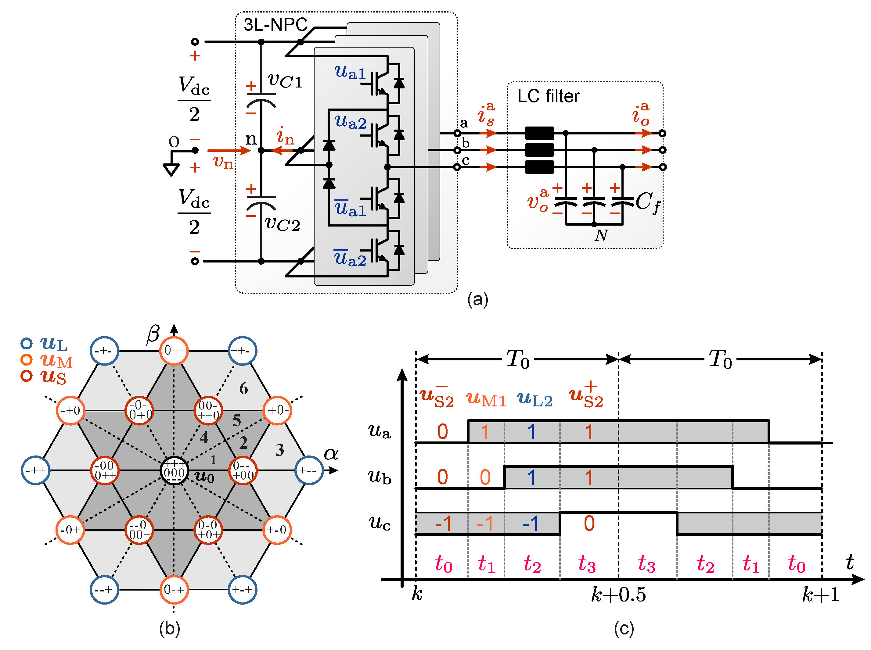
2. The 3L-NPC Inverter

The 3L-NPC inverter was the first multilevel converter topology, proposed by the group of Akagi in [29]. It was introduced around 1980 to reduce the pulsating torque and harmonic losses on AC drives, thus improving the efficiency and reducing the cost of the system. Nowadays, this converter topology is the standard for medium- and high-voltage applications [30,31]. In the mining industry, for example, 3L-NPC converters are used in variable frequency drives (VFD) for long belt-conveyor systems carrying ore [32].
As shown in the circuit diagram in Figure 1a, the 3L-NPC converter is composed of four switches and two clamped diodes per leg, producing a total of 27 three-phase switching states, u abc , for the whole converter, where u abc U { 1 , 0 , 1 } 3 . As depicted in Figure 1b, these switching states produce 19 non-redundant and 8 redundant switching vectors (SVs), u s , in the α β frame, where u s = T α β u abc and T α β is the amplitude invariant a b c -to- α β transformation [33].
According to the circuit diagram depicted in Figure 1a, the inverter voltages, v abc = v ao v bo v co , are provided by
v abc = 1 2 V dc u abc + ( 1 | u abc | ) v n
where | u abc | = | u a | | u b | | u c | and v n = 1 2 ( v C 2 v C 1 ) is the NP-voltage. Using the transformation, T α β , the inverter voltages (1) in the stationary α β frame can be expressed as
v s = 1 2 V dc u s T α β | u abc | v n .
On the other hand, for a three-phase load with a floating neutral, the NP-voltage evolves as a function of the NP-current, i n , according to
( C 1 + C 2 ) d v n d t = i n , i n = | u abc | i abc
Therefore, for a given output current, i abc = i s a i s b i s c , as shown in (3), only small- and medium-size SVs, u S and u M (see Figure 1b) respectively, can affect the NP-voltage [34]. However, to balance the NP voltage, small SVs play a significant role because the redundancy of each SV drives an NP-current of the same amplitude but in the opposite direction. This tendency impacts v n but not v s when the capacitors are balanced with a negligible voltage ripple, i.e., v n 0 .
To synthesize a desired inverter output voltage, the three nearest SVs are typically employed in carrier-based and space-vector PWM techniques [34,35]. Due to the presence of redundancies, several switching sequences (or switching patterns) can synthesize the desired output voltage. Therefore, the generation of switching sequences can be used for several purposes, such as to reduce the switching frequency and to minimize the NP-voltage ripple [34].
Based on the above analysis, the seven-segment switching sequence (7S-SS) [34] will be adopted in this work to implement the OSS–MPC strategy for voltage and current control. This switching pattern consists of four SVs, which are arranged in such a way that the transition between two adjacent switching states demands only one switching action. Additionally, each switching period is split into two sub-cycles of duration T 0 = T s / 2 , in which the disposition of the second sub-cycle is a reversal of the arrangement of the first [34], as shown in the example in Figure 1c. Furthermore, the first sub-cycle starts with an N-type small-size SV ( u S ) and ends with the P-type redundancy ( u S + ). Therefore, each 7S-SS candidate can be defined accordingly as
S u S [ t 0 ] , u 1 [ t 1 ] , u 2 [ t 2 ] , u S + [ 2 t 3 ] , u 2 [ t 2 ] , u 1 [ t 1 ] , u S [ t 0 ]
where t i is the time in which the ith switching vector is synthesized by the converter, as depicted in Figure 1c.
Since the twelve internal regions (highlighted in grey in Figure 1b) have two N-type small-size SVs, each of them is further partitioned into two sub-regions to reduce the NP-voltage ripple [34]. Thus, to determine which dominant N-type small-size SV should be utilised to assemble the desired switching sequence, the space of SVs is divided into 36 regions, as shown in Figure 1b. Then, according to the OSS–MPC principles, a 7S-SS candidate is denoted as S j , where j R { 1 , , 36 } .

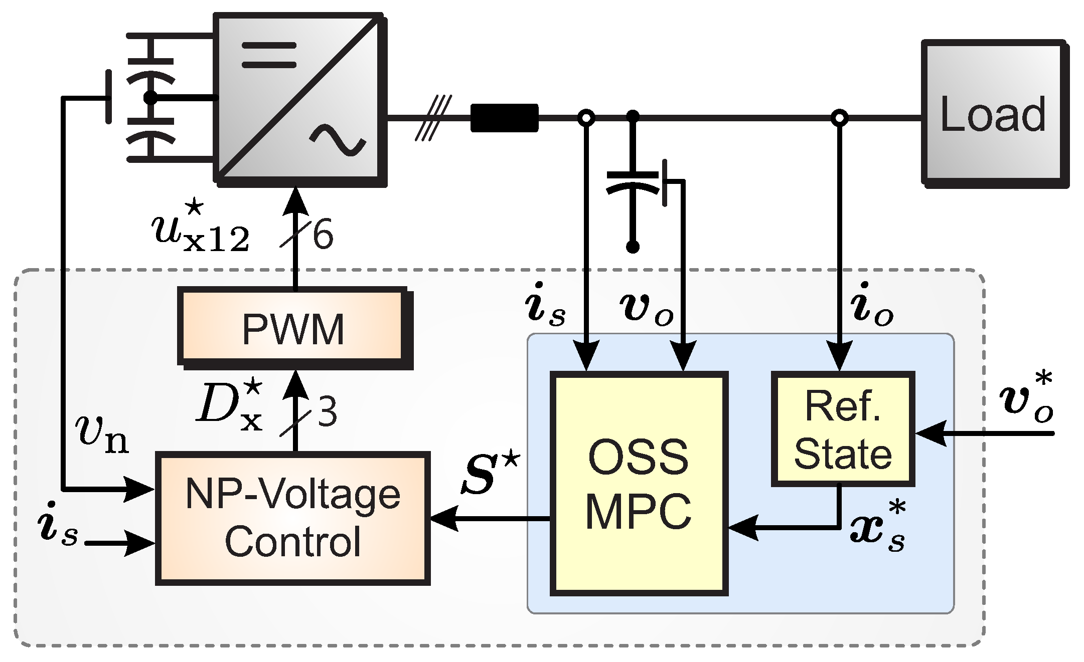
3. OSS-MPC Strategy for Voltage and Current Control

In this work, an OSS–MPC scheme will be employed to simultaneously control the voltage and current at an L C filter, while maintaining balanced voltages at the capacitors of the DC-link in a 3L-NPC converter. The overall controller is a predictive control scheme based on the solution to two optimisation problems.
The proposed control scheme is shown in Figure 2. The first optimisation problem—hereinafter called the outer optimisation loop—computes the optimal switching vectors sequence and duty cycles that minimize a cost function. The cost function is designed to track the desired values of the state vector and minimize the control effort of the converter. The second optimisation problem—hereinafter called the NP-voltage optimisation loop—computes an optimal common-mode injection signal (see bottom left-hand side of Figure 2). The common-mode injection signal is designed to balance the neutral-point voltage between the DC-link capacitors. Notice that the NP-voltage optimisation loop presented in this work has already been discussed in [26]. However, for completeness, it is briefly summarised in Section 6.

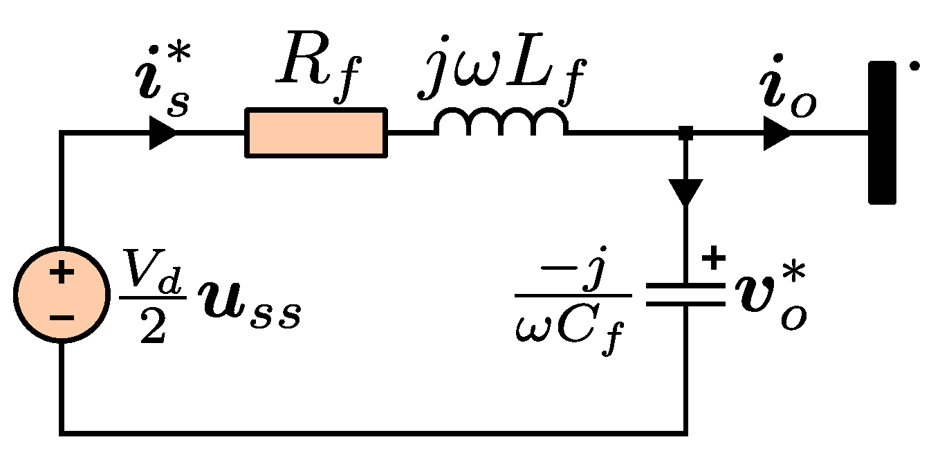
3.1. Continuous-Time Model

Let us consider a three-phase 3L-NPC converter connected to an L C filter, as shown in Figure 1a. The system of differential equations describing the dynamics of the L C filter can be written as
L f d i s α β d t + R f i s α β = v s v o α β
C f d v o α β d t = i s α β i o α β
Assuming that the DC-link NP-voltage is balanced (i.e., v n = 0 ), the converter output voltage in (2) is equal to v s = V dc 2 u s . Moreover, by rearranging the equations and defining the state, input, and disturbance vectors as x s = [ i s α i s β v o α v o β ] , u s = [ u s α u s β ] , and i o = [ i o α i o β ] (The superscripts α β in the vectors will be avoided to simplify the notation), the state-space model of the AC side dynamics is then calculated as
x ˙ s = A x s + B u s + E i o
y = C x s
Matrices A , B , and E contain the parameters of the filter and matrix C is the identity matrix.
A = L 1 R L 1 C f 1 0 B = V d c 2 L 1 0 E = 0 C f 1
The resistance, inductance, and capacitance matrices are defined as follows:
R = R f I 2 L = L f I 2 C f = C f I 2
The dimensions of the system matrices are A R 4 × 4 , B R 4 × 2 , E R 4 × 2 , x s ( t ) R 4 × 1 , u s ( t ) R 2 × 1 , and i o ( t ) R 2 × 1 .

3.2. Discrete-Time Model

MPC algorithms use the discrete-time mathematical model of the system to make predictions of the state-vector trajectory, then utilise the predicted values in an optimisation problem and compute the best control action that fulfils the control objectives.
Typically, for the discrete implementation of the continuous-time model, the forward-Euler method is applied, and this is briefly reviewed below. However, the forward-Euler methodology has some disadvantages for the control of L C -filtered stand-alone loads, and this is further discussed at the end of Section 3.2.1.

3.2.1. Forward-Euler-Based Discrete Time Model

It is assumed in this work that a 7S-SS is applied to the converter during every switching cycle. Considering the forward-Euler method, the instantaneous trajectory of the state vector when a switching vector is applied can be computed as
x s ( + 1 ) = x s + T 0 f x s , u s , i o d
where { 0 , 1 , 2 , 3 } is the index for the switching vectors of the sequence. The instantaneous evolution of the state-vector prediction at the end of the sub-cycle corresponds to its average trajectory when the seven-segment SS defined by (4) (see [24]) is applied to the system:
x ¯ s [ k + 1 ] = x s [ k ] + T 0 = 0 3 d x s d t | t = d
To simplify the analysis, every subinterval slope, m = f ( x s , u s , i o ) , is approximated using the values of the state and disturbance vector at the sampling instant, k, as m f ( x s [ k ] , u s , i o [ k ] ) . Therefore, the prediction of the average trajectory can be expressed as
x ¯ s [ k + 1 ] = A d x s [ k ] + E d i o [ k ] + B d = 0 3 u s d
where A d = I 4 + T 0 A , E d = T 0 E and B d = T 0 B . Because for any N-type seven-segment SS, u s 0 = u S , and u s 3 = u S + , the duty cycles d 0 and d 3 can be combined as d s = d 0 + d 3 , which is the duty cycle for the small vectors of the sequence [24]. Then, the following linear representation of the average trajectory can be stated as
x ¯ s [ k + 1 ] = A d x s [ k ] + E d i o [ k ] + B d U d
where the dwell-time vector, d , and switching matrix, U , are defined as
d = d s d 1 d 2 D 0 , 1 3
U = u s u 1 u 2
Even when the forward-Euler discretisation algorithm is widely used for the implementation of MPC algorithms, there are some issues which are produced when this methodology is applied to L C -filtered stand-alone loads. Some of these issues are as follows:
  • For these sort of applications, usually two cascaded MPC algorithm are implemented [36] to regulate the voltages and currents. An outer MPC regulates the voltages and an inner MPC regulates the converter’s output currents; in this case, the standard forward-Euler algorithm performs well. Nevertheless, when nested cascaded MPC loops are implemented, two cost functions are required and a global optimum is not necessarily reached. This is further discussed in [37].
  • To obtain a global optimum, a single cost function is recommended, which has to consider the tracking errors of the currents and load voltages. However, an L C -filtered load is a plant which is not reachable in a single-step horizon, i.e., the output currents and load voltages cannot reach their reference values in one step because the B matrix of (11) is not squared (see [28]). To solve this issue when the forward-Euler discretisation method is used, an MPC algorithm with a two-step horizon has been proposed in [37]; nevertheless, this larger prediction horizon may produce a relatively large computer burden, which can be justifiable for a large and costly modular multilevel converter but is hardly convenient for a smaller stand-alone application.
  • Moreover, one of the main disadvantages of forward-Euler-based MPC algorithms for single-stage implementation (i.e., the application presented in this work) is the unconstrained solution obtained from the cost solution of (30). The matrices A d and B d obtained using the forward-Euler discretisation method (see (12)) are prone to producing an unconstrained solution for U d which is very weakly related to the load-voltage tracking error. Therefore, when forward-Euler is applied to the system of Figure 1b, poor performance or even a complete lack of control could be obtained for the regulation of the load voltage. Conversely, when the improved-Euler method is used to discretise (6a) and (6b), more exact matrices are obtained for A d and B d (see (17)) and the unconstrained solution for U d can be tuned (by adjusting the cost weights) to be dependent on both the tracking error of the load voltage as well as on the tracking error of the 3L-NPC converter output current.
Based on the comparison presented above, in this work the discretisation of the continuous-time model is performed using the improved-Euler method [38]. This is further discussed in the next section.

3.2.2. Improved-Euler-Based Discrete Time Model

The improved-Euler method is a second-order Runge–Kutta method to compute the solutions of ordinary differential equations [38]. In this method, the weighted average of the approximations to the derivative at intermediate points on the solution curve is computed. Specifically, the improved-Euler method uses the extreme points of the solution interval (i.e., kth and ( k + 1 )th points). Higher-order Runge–Kutta methods use more intermediate points to increase the accuracy of the solution.
Once again, it is assumed that a 7S-SS is applied by the converter during the complete switching cycle. Considering the improved-Euler method, the instantaneous evolution of the state vector is given by the following equation:
x s + 1 = x s + T s 2 f x s , u s , i o + f x s [ k + 1 ] , u s [ k + 1 ] , i o [ k + 1 ] d
The average slope is multiplied by T s because it is the time length between predictions in the interval [ k , k + 1 ] and predictions in the interval [ k + 1 , k + 2 ] . To simplify (14), some assumptions about the states and inputs used for computational purposes are required. Firstly, the slope of the system at the kth time instant is computed with the values measured at the time instant k (i.e., f x s , u s , i o f x s [ k ] , u s , i o [ k ] ). Secondly, the slope at the ( k + 1 )th time is computed with the predicted state vector, x ¯ s [ k + 1 ] , using the forward-Euler approximation defined by (12). The switching sequence applied is the same as that of time instant k (i.e., f x s [ k + 1 ] , u s [ k + 1 ] , i o [ k + 1 ] f x ¯ s [ k + 1 ] , u s , i o [ k + 1 ] ). The disturbance vector is assumed to be constant during the switching cycle but different between switching cycles (i.e., i o [ k ] i o [ k + 1 ] ). Considering these assumptions, the state-vector trajectory is described by
x s + 1 = x s + T s 2 [ f x s [ k ] , u s , i o [ k ] + f x s [ k + 1 ] , u s , i o [ k + 1 ] ] d
The slopes m [ k ] = f x s [ k ] , u s , i o [ k ] and m [ k + 1 ] = f x ¯ s [ k + 1 ] , u s , i o [ k + 1 ] are described by the following equations:
m [ k ] = A x s [ k ] + B u s + E i o [ k ]
m [ k + 1 ] = A x ¯ s [ k + 1 ] + B u s + E i o [ k + 1 ]
Replacing x ¯ s [ k + 1 ] in (16b), the expression for the slope m [ k + 1 ] is obtained as follows:
m [ k + 1 ] = A + 1 2 T s A 2 x s [ k ] + 1 2 T s A B U d + 1 2 T s A E i o [ k ] + B u s + E i o [ k + 1 ]
Then, the average trajectory of the state vector, using the improved-Euler method, is computed as
x ¯ s [ k + 1 ] = x s [ k ] + T s 2 = 0 3 [ m [ k ] + m [ k + 1 ] ] d
Replacing (16a) and (17) into (18), and after some algebraic manipulations, the following expression is obtained:
x ¯ s [ k + 1 ] = I + T s A + 1 4 T s 2 A 2 x s + I + 1 4 T s A T s B U d + 1 2 I + 1 2 T s A T s E i o [ k ] + 1 2 T s E i o [ k + 1 ]
Equation (19) is useful when an observer-predictor computes i o [ k + 1 ] , and the difference between i o [ k ] and i o [ k + 1 ] is sufficiently large. However, if it is assumed that i o [ k ] i o [ k + 1 ] then the average prediction model is simplified to
x ¯ s [ k + 1 ] = I + T s A + 1 4 T s 2 A 2 x s + I + 1 4 T s A T s B U d + I + 1 4 T s A T s E i o [ k ]
The discrete-time model in (20) can be written as the linear representation (12) with A d = I + T s A + 1 4 T s 2 A 2 , B d = I + 1 4 T s A T s B , and E d = I + 1 4 T s A T s E . This discrete-time model will be used in this work.

4. OSS-MPC Formulation for Voltage and Current Control

The main objective of the controllers is to keep the voltage of the L C filter capacitors as sinusoidal non-distorted waveforms. Meanwhile, the converter currents are controlled as a secondary objective. In this regard, the reference voltage vector is
v o * [ k + 1 ] = V * e j ω [ k + 1 ] T s
where V * is the magnitude of the reference voltage vector and ω is the fundamental frequency of the output voltage ( ω = 2 π f 0 ).
The reference current is obtained as a function of the reference voltage. Replacing the reference voltage vector into the dynamic equation of the output voltages yields [39]
d v o * d t = 1 C f i s * i o
Solving the equation for i s * , the converter reference current vector is obtained:
i s * = ω C f J v o * + i o
where the matrix J is defined as
J = 0 1 1 0
It is desirable to constrain the reference current to a maximum value, I m a x . When the amplitude of the reference current is less than the specified limit, the reference current vector is described by Equation (23). In the other case, the reference current vector is saturated at I m a x . Therefore, the constrained reference current is represented by the following piece-wise function:
i s * = ω C f J v o * + i o i s * 2 < I m a x I m a x i s * 2 i s * i s * 2 I m a x
Thus, the reference state vector is
x s * [ k + 1 ] = i s * v o *

4.1. Cost Function

At the heart of the MPC strategy lies the cost function. In the cost function, the variables related to the control objectives are weighted to choose the best possible action. In FCS-MPC schemes, the cost function is most commonly designed to minimize the tracking error [5,16]; however, it has been shown that FCS-MPC strategies without penalization of the control effort are equivalent to quantised deadbeat controllers [19]. Deadbeat controllers feature fast dynamic response [28], but they have poor robustness against model mismatches, parameter uncertainties, and noise on measured variables [40]. To alleviate the unwanted effects of deadbeat controllers, the control effort is usually penalised in the cost function [28]. In the control proposed in this work, the OSS–MPC control has two objectives: minimise the tracking error between the state vector and its reference and penalize the control effort. Therefore, the following cost function is defined:
J ( U j , d j ) = x s [ k + 1 ] x s * [ k + 1 ] Q 2 + λ u u [ k ] u s s [ k ] 2 2
The positive-definite matrix Q = diag( λ i , λ i , λ v , λ v ) is used to trade-off the control objectives of the state-vector tracking. Similarly, the weighting factor, λ u , is used to penalize the control effort. The optimisation variable of the problem is the average switching vector, u ( k ) . The average switching vector is the product between the switching matrix and the duty cycle vector, u ( k ) = U d .
Firstly, the term of the cost function used to penalize the reference tracking error will be reformulated as a function of the average switching vector, u ( k ) . Replacing (12) in (27) yields
B d u x s * [ k + 1 ] A d x s [ k ] E d i o [ k ] : = κ [ k ] Q 2
where the value of κ can be obtained using (12). If x s * [ k + 1 ] = A d x s [ k ] + E d i o [ k ] + B d U d , then the required B d U d to produce x s * [ k + 1 ] is equal to x s * [ k + 1 ] A d x s [ k ] E d i o [ k ] . This is defined as κ in (28).
The second term of the cost function in Equation (27) has the vector u s s . Vector u s s is the steady-state control action. The steady-state control action is the input vector needed to drive the system towards the steady-state solution. The expression for this vector is obtained by solving the circuit of Figure 3 for u s s . The steady-state control input, u s s , is defined as
u s s = 2 V d c { [ 1 ω 2 L f C f I 2 + ω R f C f J ] v o * + [ R f I 2 + ω L f J ] i o }
Finally, the cost function for the optimisation problem can be written as
J j ( U j , d j ) = B d u [ k ] κ Q 2 + λ u u [ k ] u s s [ k ] 2 2

4.2. Optimisation Problem
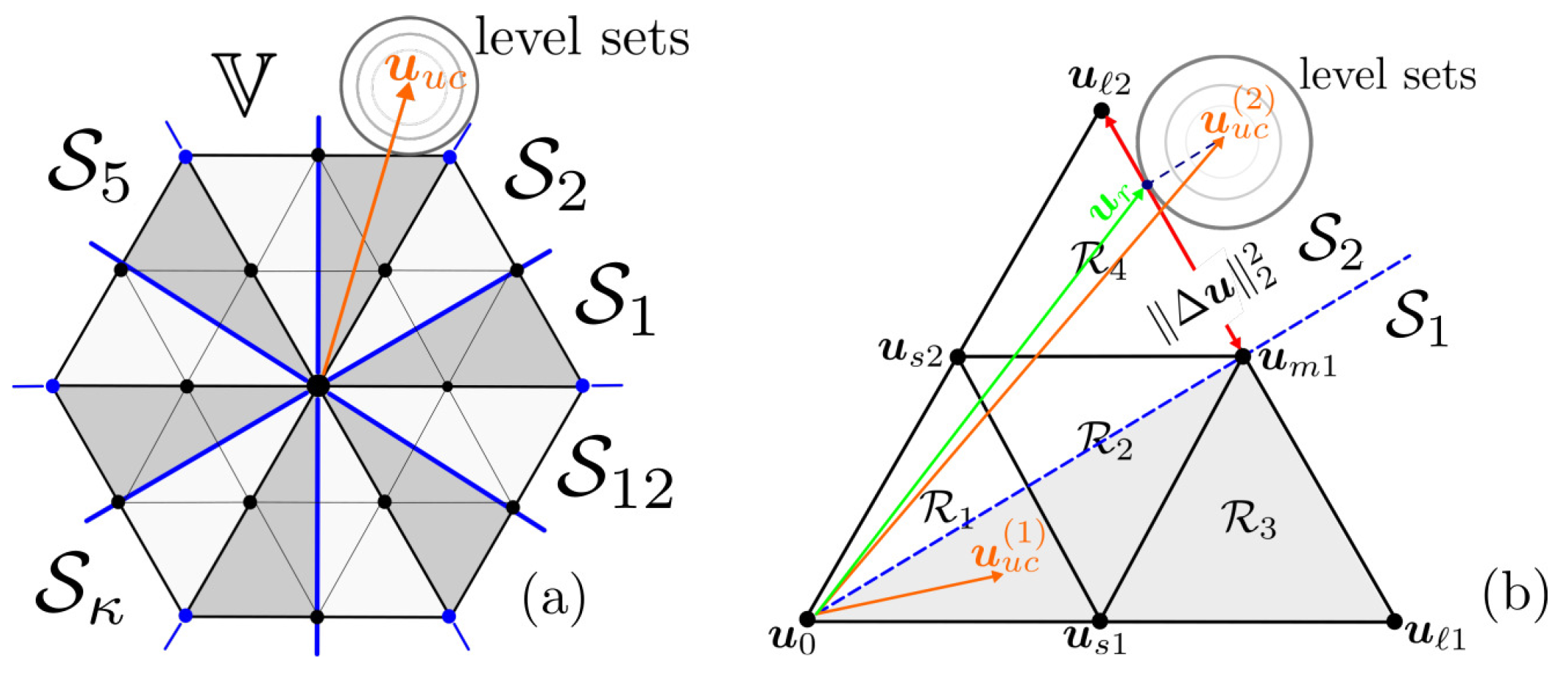
In OSS–MPC, the optimal switching sequence (OSS) is obtained by solving an optimisation problem. The solution must comply with constraints such that the sum of leg duty cycles is equal to one, and each duty cycle must be equal to or greater than zero. Therefore, the optimisation problem to be solved is as follows:
{ U , d } = arg min U j { min d j J j ( U j , d j ) }
s . t . 1 d = 1
d j 0
The optimisation problem has the same form as the one solved in [26]. Therefore, the same optimiser will be used. Thus, the usual strategy to solve MPC problems with 3L-NPC converters of evaluating each region, R j { R 1 , , R 24 } , of the space of vectors is avoided.

5. Optimal Solution

In this section, the optimisation problem presented in (31a), (31b) and (31c) will be solved to obtain the optimal switching vector sequence and its corresponding duty cycles to be applied during the next sampling instant. Two cases of the problem are distinguished: first, the linear modulation stage where the duty cycles are positive, and second, the overmodulation stage where the duty cycle of the small switching vectors becomes negative.

5.1. Non-Negative Duty Cycles: The Linear Modulation Stage

To relax the optimisation problem, the inequality constraints are removed from the problem formulation. Thus, the solution is assumed to be in the linear modulation stage, where the duty cycles are always non-negative. The relaxed optimisation problem is then stated as
min d J j ( U j , d j )
s . t . 1 d j = 1
Expanding the cost function (30) yields
J j = B d u κ Q B d u κ + λ u u u s s u u s s
The following expression is obtained:
J j = u Q + λ u I 2 u 2 u B d Q κ + λ u u s s + λ u u s s u s s + κ Q κ
where Q is the modified weight matrix, Q = B d Q B d . The elements of the switching matrix, U j R 2 × 3 , are the vectors of the switching sequence:
U j = u s α u 1 α u 2 α u s β u 1 β u 2 β
Considering the equality constraint of the relaxed optimisation problem, the duty cycles for the small switching vectors, as a function of the remaining duty cycles, can be written as
d S j = 1 d 1 j d 2 j
An auxiliary variable, d η j , is defined to eliminate the dependent variable d S from the optimisation vector d j :
d η j = d 1 j d 2 j
The relationship between d j and d η j is as follows:
d j = 1 1 1 0 0 1 M d η j + 1 0 0 N
Then, u = U d = U M d η j + N = U M d η j + U N and u = d U = M d η j + N U = d η j M + N U . The cost function in terms of d η j is
J = d η j M U Q + λ u I 2 U M d η j + 2 d η j M U Q + λ u I 2 U N 2 d η j M U B d Q κ + λ u u s s + N U Q + λ u I 2 U N 2 N U B d Q κ + λ u u s s + κ Q κ + λ u u s s u s s
Computing the gradient of J with respect to d η j and making it equal to zero yields
J d η j = 2 M U Q + λ u I 2 U M d η j + 2 M U Q + λ u I 2 U N 2 M U B d Q κ + λ u u s s = 0
Reorganizing (40) to leave the terms related to the duty cycles on the left, (41) is obtained:
M U Q + λ u I 2 U M d η j = M U B d Q κ + λ u u s s M U Q + λ u I 2 U N
Solving the equation for d η j yields
d η j = U M 1 u u n c U M 1 U N
Therefore, the unconstrained control action ( u u c ) is defined as
u u c = Q + λ u I 2 1 B d Q κ + λ u u s s
Now, it is necessary to map the solution back to its original variables. Replacing (42) in (38) yields
d r j = M U M 1 N M U M 1 U N u u c 1
The optimal duty cycles for the linear modulation stage are computed using the ( 3 × 3 ) matrix:
d r j = 1 Δ u 1 β u 2 β u 2 α u 1 α u 1 × u 2 u 2 β u s β u s α u 2 α u 2 × u s u s β u 1 β u 1 α u s α u s × u 1 u u c , α u u c , β 1
where Δ is the determinant of matrix product U M 1 :
Δ = u S × u 1 + u 2 × u S + u 1 × u 2
with u x × u y = u x α u y β u x β u y α denoting the cross product.

5.2. Handling the Negative Duty Cycles: The Overmodulation Stage

In the previous section, the relaxed solution to the optimisation problem was calculated. The relaxed duty cycles vector, d r j , is the local solution for each region, R j R , of the control hexagon, V . The relaxed solution computed with (32a) and (32b) fulfills the equality constraint 1 d = 1 . Thus, all regions can be mapped onto u u c in the α β -plane. However, only one region fulfils the non-negativity constraint [24]. The non-negativity constraint can then be considered in the solution with a simple methodology (as reported in [24,26]). The methodology introduced therein also reduces the computational burden, avoiding the search over all 24 regions of the control region V to only four. The methodology will be explained in this section.
Firstly, considering the α β -plane shown in Figure 4a with the space of vectors of the 3L-NPC converter is divided into 12 regions. The algorithm seeks the region where u u c is located, and then the three sectors in that region are evaluated in the control algorithm. Given that u u c is the desired solution of the optimisation problem, its angle is used to find the optimal region in the plane. The optimal sector, S , is obtained from the following equation:
S = floor { 6 π tan 1 u u c , β u u c , α } + 1
When the optimal sector is calculated, the duty cycles of the switching sequences contained in it are evaluated. The sector whose duty cycles complies with the non-negativity constraint is the optimal sector, and thus the optimal switching sequence is found.
The conventional enumeration algorithm can be reduced to only three regions after the sector has been identified. Each sector has three candidate switching sequences, but only one of them fulfils the non-negativity constraint. Thus, the optimal pair { U , d } is found by evaluating the non-negativity condition over the duty cycles vector of each candidate region. However, if u u c falls outside control region V (e.g., see u u c ( 2 ) in Figure 4b) then none of the candidate switching sequences fulfil the non-negativity constraint.
The aforementioned case occurs during a transient operation. The candidate switching sequence is then reduced to one and is built by the medium and large switching vectors belonging to the only outer region that intersects the optimal sector. The case is further analyzed in the next subsection.

5.2.1. Relaxed Optimisation Problem

The unconstrained average switching vector goes outside the hexagon, thus the duty cycle for the small switching vector becomes negative. Defining d S j = 0 , the optimisation variable becomes
d j = 0 d 1 j d 2 j
Consider the equality constraint
1 0 d 1 j d 2 j = 1
Notice that one of the two optimisation variables is dependent. Thus, if we set d 2 j to be dependent of d 1 j , we can find an auxiliary vector to reduce the equality-constrained optimisation problem into an unconstrained optimisation problem:
d j = 0 1 1 M d 1 j + 0 0 1 N
Then, u = U d = U M d j + N = u 1 u 2 d 1 + u 2 and u = d j U = M d j + N U u 1 u 2 d 1 + u 2 . The cost function is
J = u 1 u 2 Q + λ u I 2 u 1 u 2 d 1 2 + 2 u 1 u 2 Q + λ u I 2 u 2 d 1 2 u 1 u 2 B d Q u d b + λ u u s s d 1 + u 2 Q + λ u I 2 u 2 2 u 2 B d Q κ + λ u u s s + κ Q κ + λ u u s s u s s

5.2.2. Solution of the Relaxed Optimisation Problem

The unconstrained optimisation problem is solved by setting to zero the derivative of the cost function with respect to the optimisation variable:
d d ( d 1 j ) J = 2 u 1 u 2 Q + λ u I 2 u 1 u 2 d 1 + 2 u 1 u 2 Q + λ u I 2 u 2 2 u 1 u 2 B d Q κ + λ u u s s = 0
Solving this for d 1 yields
d 1 = u 1 u 2 B d Q κ + λ u u s s u 1 u 2 Q + λ u I 2 u 1 u 2 u 1 u 2 Q + λ u I 2 u 2 u 1 u 2 Q + λ u I 2 u 1 u 2
The matrix Q + λ u I 2 corresponds to a scalar multiplied by the identity matrix. Bearing on mind that u u c = Q + λ u I 2 1 B d Q κ + λ u u s s , the optimal duty cycle, d 1 , is
d 1 j = ( u 1 u 2 ) ( u u c u 2 ) ( u 1 u 2 ) ( u 1 u 2 )
Notice that the denominator of d 1 j is the length between a large and the medium vector in the hexagon frontier (see Figure 4b), thus,
Δ u 2 2 = ( u 1 u 2 ) ( u 1 u 2 ) = 4 9
Then, the optimal solution for the overmodulation stage is:
d 1 j = mid { 0 , 9 4 ( u 1 u 2 ) ( u u n c u 2 ) , 1 }
d 2 j = 1 d 1 j

6. NP-Voltage Control and PWM Modulator

The objective of the NP-voltage control loop is to compute an optimal common-mode signal, u 0 , to balance the DC-link capacitors of the 3L-NPC converter.
The strategy assumes that a PWM stage is used to synthesize the solution obtained from the outer optimisation loop. To this end, the OSS S is mapped into a three-phase reference signal, D a b c = [ D a D b D c ] [ 1 , 1 ] 3 , obtained as [26]
D a b c = d 1 u a b c , 1 + d 2 u a b c , 2 + 1 2 d S u a b c , 0 + u a b c , 3
in which u a b c , = T α β 1 u s are the three-phase switching states that produce the OSS.
Finally, the three-phase reference signals sent to the PWM modulator are
D a b c = D a b c + u 0
where u 0 is the optimal common-mode signal to be injected to reduce the NP-voltage tracking error. For further analysis and discussion of the methodology proposed to obtain the common-mode signal, the reader is referred to [26].

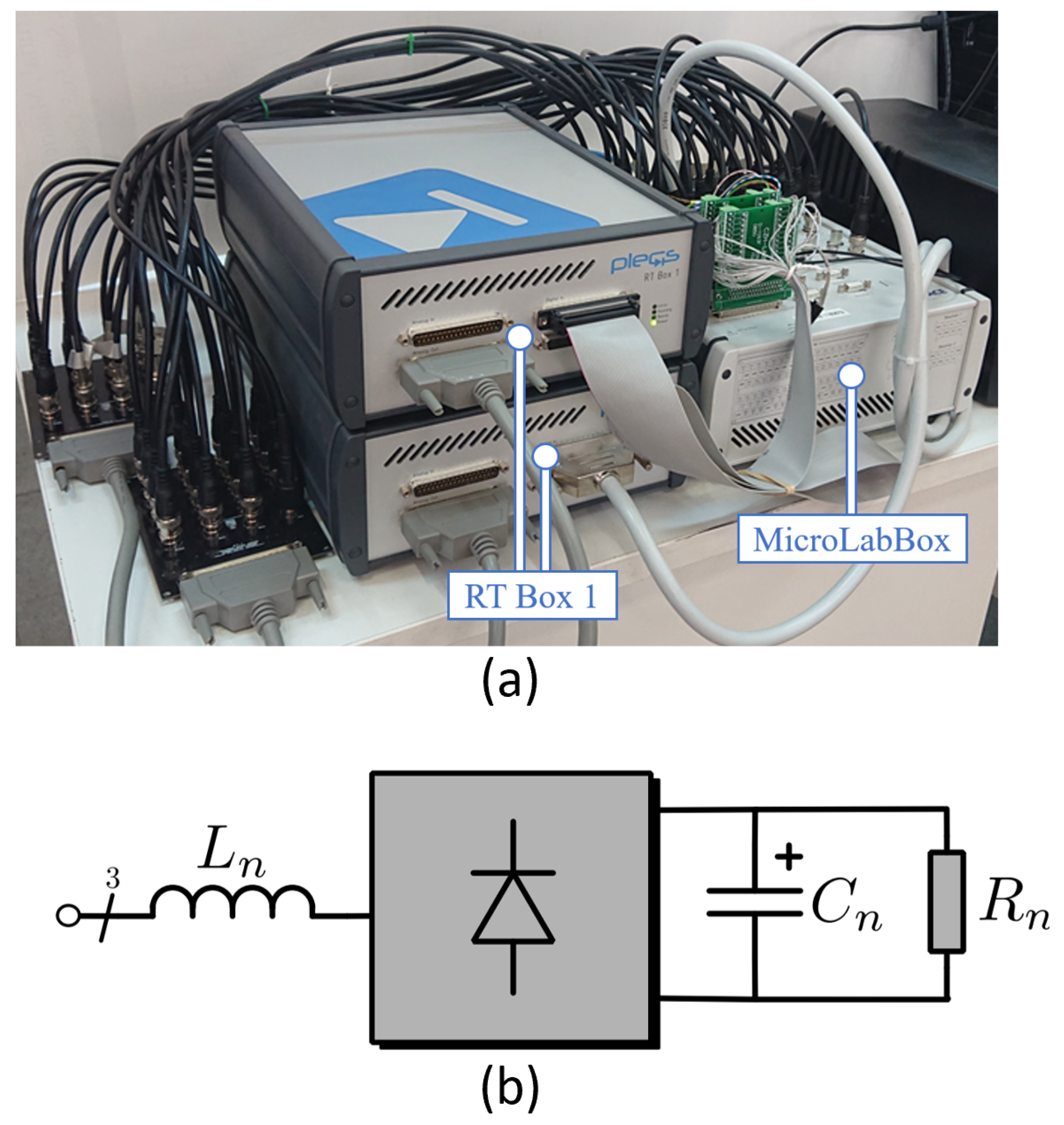
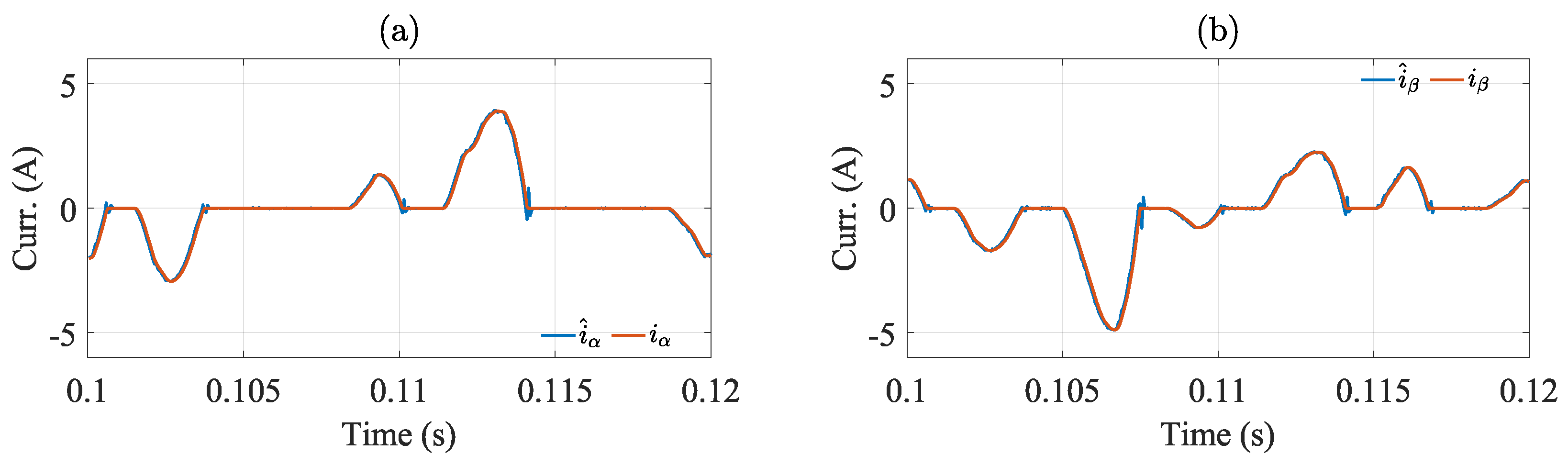
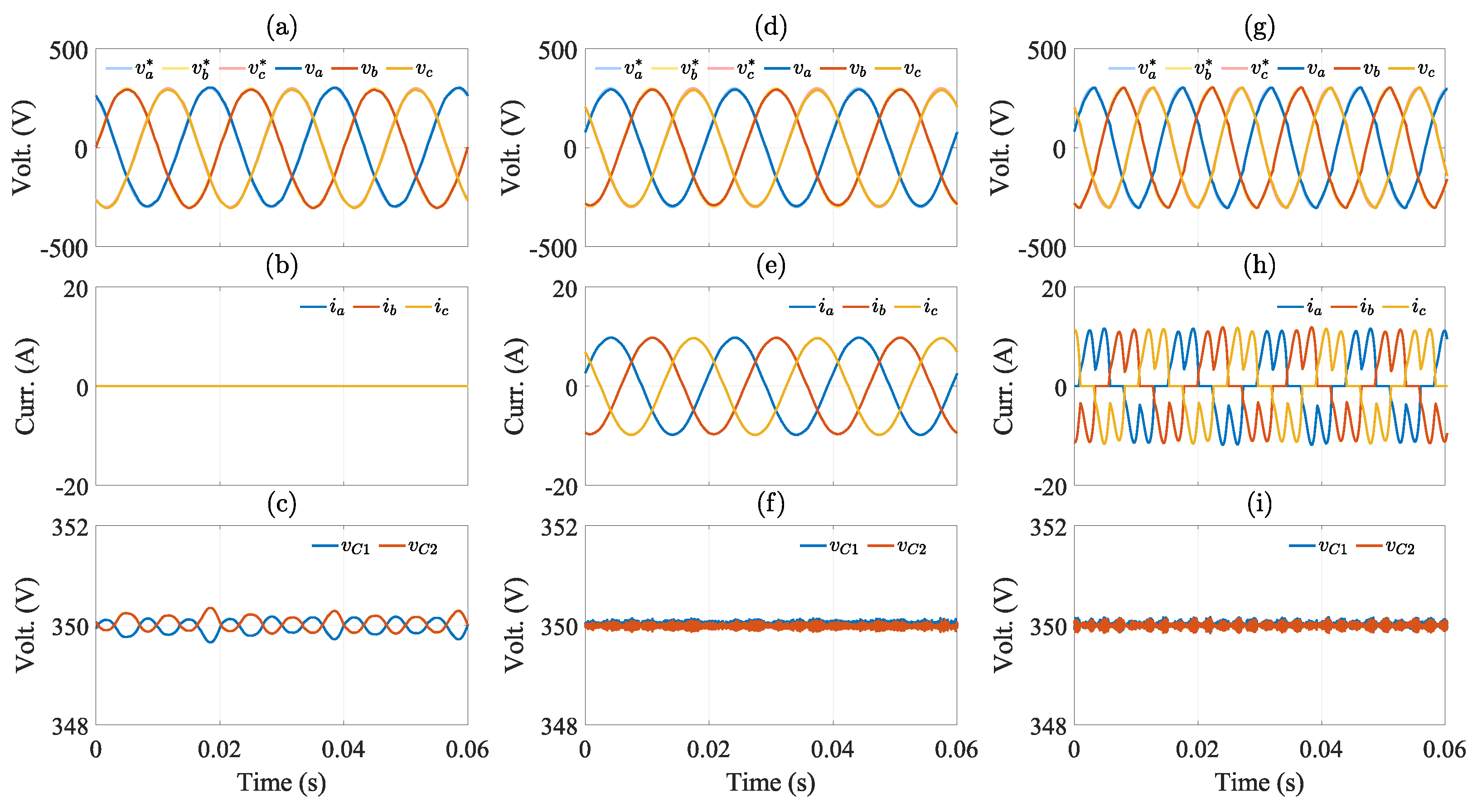
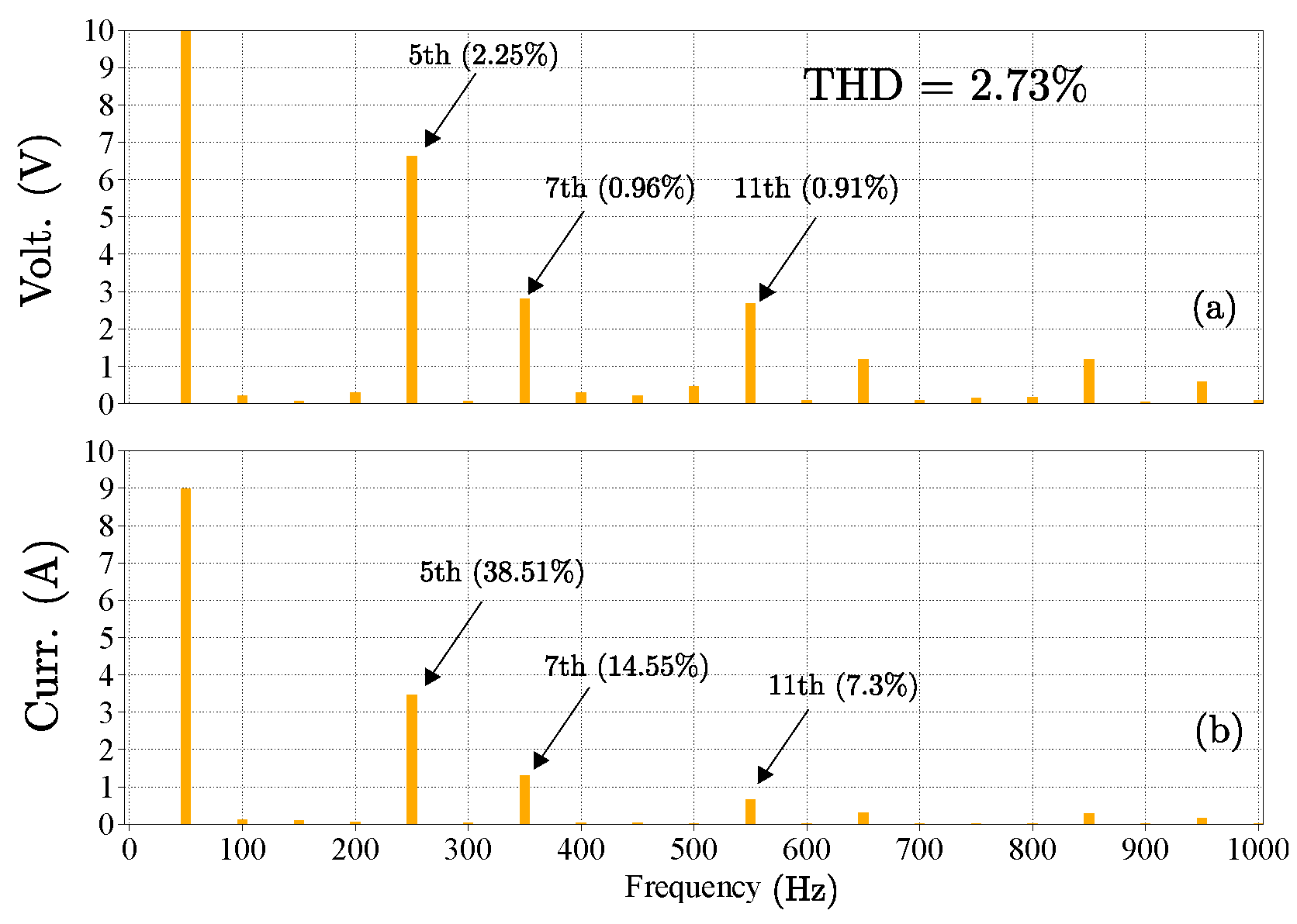
7. Hardware-in-the-Loop (HIL) Results

In this section, hardware-in-the-loop (HIL) results are shown to validate the proposed controller. The 3L-NPC converter, L C filter, and loads are emulated using PLECS-RT box 1 HIL platforms with a time-step of 5 μ s. The control system is separately implemented using a dSPACE MicroLabBox platform. This dSpace controller is equipped with a Freescale QorIQ P5020 dual-core 2 GHz processor (DSpace Gmbh, Paderborn, Germany), for number crunching, and a Kintex-7 XC7K325-T FPGA. The FPGA handles the AD conversion, performs an in-phase disposition PWM strategy, and implements a dead time of 1 μ s for each switching device; the HIL system is shown in Figure 5a. The processor computes the Clark transform of the measured three-phase variables, executes the optimisation algorithm, and computes the appropriate three-phase reference signals for the modulator. The loads considered for the study are a three-phase resistive load bank and a nonlinear load implemented using a three-phase diode rectifier with a capacitor and resistor connected in parallel at the DC side, as shown in Figure 5b. The parameters of the system are shown in Table 1 and are similar to those used in a previous work (see [27]).
For the HIL results discussed in this section, the current of the nonlinear load used in some tests, corresponds to that shown in Figure 6; notice that the non-linear current is estimated in the processor using the auto-regressive model provided by the Lagrange polynomial shown in Equation (61). For the results shown in Figure 7, Figure 8, Figure 9 and Figure 10, the weight related to the control effort is set to λ u = 0 . The effects of using different values of λ u in the performance of the proposed control system are discussed using Figure 11 and Figure 12.
The performance of the controllers is evaluated using the following goodness factors: RMS error (RMSE), percentage of voltage error ( E v ), and total harmonic distortion (THD). The percentage of error is defined as follows:
E v [ % ] = 100 v * 1 N p k P v ( k ) v * ( k ) 2 2
where P = { 1 , 2 , , N p } is the set of indices of the measurements vector and N p = T 1 / T s is the total number of elements in the vector. T 1 is the period of the fundamental frequency and T s is the period of the sampling frequency. Whenever the desired reference amplitude is unknown, the root-mean-square error (RMSE) will be used. The RMS error is defined as follows:
RMSE ( x x * ) = 1 N p k P x ( k ) x * ( k ) 2 2
A one-step delay compensation is carried out to compensate for the computational delay introduced by the digital platform. The state vector, x s [ k + 1 ] , is computed using (20) with the values measured at the kth instant and the switching sequence applied during the previous switching interval. The voltage reference, v o [ k + 1 ] , is computed by shifting the phase of the reference signal one step ahead. The load output current, i o [ k + 1 ] , is estimated using the Lagrange extrapolation technique. The Lagrange extrapolation technique uses the actual and past measurements of the signal to estimate its future value. The load output current, i o [ k + 1 ] , is computed as follows [41]:
i o [ k + 1 ] = 4 i o [ k ] 6 i o [ k 1 ] + 4 i o [ k 2 ] i o [ k 3 ]
The estimated load output current has an RMS error of 0.0603 (A) in the α -component, and 0.0640 (A) in the β -component for the worst-case scenario (nonlinear load). The estimated and measured load output current are shown in Figure 6. As shown in this figure, the estimated current tracks the measured current relatively well.
In Figure 7a, the output voltages when the system operates without load are shown. The reference voltage has an amplitude of 300 V with a frequency of 50 Hz. For this condition, the load output voltages have a voltage error of 2.04% and a THD of 1.74%. Then, a three-phase resistive load is connected as in Figure 7d. In this condition, the voltage error is 2.05% and the THD is 1.03%. When a nonlinear load is connected, as in Figure 7g, the voltage error is 2.83%. The harmonic spectrum for the load output voltage and load output current are shown in Figure 8a,b. The voltage THD in this case is 2.73% with the presence of 5th and 7th harmonics, which are produced by the bridge rectifier. In Figure 7b–h, the load output current is shown for the three aforementioned cases. Finally, in Figure 7c–i the DC-link capacitor voltages are shown. The control strategy is capable of keeping the DC-link voltages balanced and well regulated for all operating conditions, with very small oscillations.
The transient operation of the controlled system is studied in Figure 9, considering changes in the reference voltage amplitude with λ u = 0 . The variables are presented in the synchronous reference frame to verify the settling time of the load output voltage.
The settling time is computed as the time required by the output voltage to reach and stay within 5% of the desired voltage. In Figure 9a, the reference voltage receives a step variation from 300 V to 100 V at t = 0.2 s. The voltage error amounts to 5.98% under steady-state conditions. The rise in voltage error results from the reduction in the amplitude of the reference voltage. In Figure 9b, the reference voltage varies from 100 V to 300 V at t = 0.2 s. In this case, the load output voltage manages to stay within the band of 5% around the desired voltage. Thus, the settling time is approximately 1.03 ms.
Notice that a relatively low steady-state error is presented in the HIL results shown in Figure 9a,b. This small steady-state error is produced because there is not an integrator in the MPC algorithm [42,43]. If the steady-state error is a must, then the state-space matrix, A (see (7)), must be augmented with additional states to represent the integrator [42]; however, this topic is considered to be outside the scope of this work.
Figure 10 shows the operation of the system for a load step. A dip occurs in the load output voltage, as shown in Figure 10a, and takes approximately 1 ms to recover. Notice that there is a sudden increase in the inductor reference current to approximately 10 A, and the current features a fast dynamic response to the step change.
The cost function of (30) has two terms: the first term penalizes the deviation of the system states from a reference vector and the second term penalizes the control effort of the converter. The control effort is penalized in the cost function by the deviation between the optimisation variable, u ( k ) , and the steady-state control effort, u s s . The weight of this deviation on the optimisation problem is set by the parameter λ u . Increasing λ u will lead the converter’s response to move closer to open-loop operation since u s s depends only on the load reference voltage and load output current. The system’s performance with a logarithmic variation of parameter λ u is shown in Figure 11. The results are obtained considering a three-phase resistive load at the L C filter terminals. The best trade-off in terms of voltage error between open-loop and closed-loop operation of the converter is achieved when λ u = 10 , as shown in Figure 11a. When λ u is increased, the response of the system tends toward u s s , which does not penalize the voltage error. Thus, the voltage error increases.
As shown in Figure 11b, the voltage THD presents slight variations around 1%, as shown in Figure 11b. The system’s transient response is also dependent on the value of λ u . A trade-off between settling time and overshoot must be reached, as shown in Figure 12. Increasing λ u up to 100 will reduce the settling time of the system but increase the voltage overshoot. However, for λ u > > 100 , the system response will present a damped sinusoidal oscillation which increases the settling time.

8. Comparison with a Previously Reported OSS-MPC Algorithm

In this section, the proposed scheme is compared with the prior OSS–MPC method discussed in [27]. In that publication, it is proposed to regulate the voltage in the L C -filtered load without considering a term weighting the control effort. This is similar to using λ u = 0 in (30). In addition to ignoring the control effort, regulation of the converter’s output current is not considered in [27]. For the comparison, simulation work using PLECS 4.7 software has been performed.
Figure 13 shows simulation results considering a step change from 0 to 300 V in the load voltage for both control strategies, i.e., the one published in [27] and that proposed in this work. In this case, the value λ u in (30) has been set to 0. As shown in Figure 13a, the proposed method presents neither overshoot nor noticeable oscillation in the load voltages, as opposed to the results obtained with the OSS–MPC of [27] (see Figure 13a,c). The smooth transition in the load voltage is obtained by the utilisation of the cost function of (30), which considers the inductor current and output voltage tracking errors. Moreover, the utilisation of a term in the cost function weighting the output-current tracking error produces a considerably smaller current peak (16.35 A, see Figure 13b) when compared to the 32.1 A obtained for the method of [27] (see Figure 13d). The proposed method also has a slightly faster response, taking 0.81 ms to reach steady-state in Figure 13. Meanwhile, the prior OSS–MPC method takes 0.83 ms to reach steady-state.
An amplified view of Figure 13 is shown in Figure 14. The effects produced by neglecting an output current-related term, in the cost function of [27], are clearly shown in Figure 14c,d. A large peak current, as well as relatively large undamped current oscillations, are produced for ≈1.2 ms after the step change. These large current oscillations affect the quality of the load-output voltage. Notice the smooth variation in the output voltages produced when the control method proposed in this work is applied. This is shown in Figure 14a,b.
The performance of the control systems has also been tested considering a balanced load step of 30 Ω in t = 0.1 s. Before the step, the system is operating without a load parallel connected with the capacitor of the L C -filter. Figure 15a,b shows the performance obtained with the OSS–MPC strategy proposed in this work; meanwhile, Figure 15c,d shows the results obtained with the work reported in [27]. Again, the peak current overshot shown in Figure 15b is smaller than that of Figure 15d, with peak values of approximately 14.5 A and 21.5 A, respectively. The control strategy of [27] has a smaller dip in the load voltage for the step in t = 0.1 s; however, this better performance is obtained because neither the control effort nor the peak currents are considered in the cost function reported in that work. Moreover, as discussed previously for the results presented in Figure 14d, lightly damped current oscillations are produced after the load step, as depicted in Figure 15d. These current oscillations also affect the load voltage, as shown in Figure 15c, for the time immediately after t = 0.1 s. It is concluded that, for the load step change, the performance of the proposed control system is better than that of [27], which is shown in Figure 15c,d. The peak current is lower and the lightly damped oscillations in the currents and voltages are completely avoided, as depicted in Figure 15a,b.
The performance of the proposed control system is also clearly superior to that reported in [27], when the nonlinear load of Figure 5b is connected at the output of the L C -filter. The simulation results are shown in Figure 16a,b; before t 0.05 , the capacitor at the nonlinear load is completely discharged and it is equivalent to a short circuit immediately after the nonlinear load is connected at t 0.05 s. Therefore, the control system reported in [27] has a bad performance because neither current control nor current limitation is considered in the cost function reported in that paper. Hence, the current shown in Figure 16b reaches a peak value of 297.2 A; meanwhile, the peak current achieved by the OSS–MPC algorithm reported in this work is 33 A. Of course, with this large current the control strategy of [27] manages to regulate the load voltage in approximately 20 ms vs. 80 ms for the proposal, but it is unlikely that the power converter and L C filter could withstand this large output current surge. Therefore, the lack of current regulation is certainly a very strong drawback of the control strategy being compared with the MPC scheme reported in this work.

9. Conclusions

In this paper, an optimal switching sequence MPC algorithm was proposed for a three-level neutral-point-clamped inverter with an output L C filter. The strategy is an extension of the cascaded optimal switching sequence MPC proposed in the literature for current and direct power control of active front-end 3L-NPC inverters. The control objectives of the algorithm were twofold: (1) achieve good tracking performance for the L C filter variables (current and voltages) and (2) maintain a balanced neutral-point voltage between the DC-link capacitors of the converter using the algorithm already reported in [26]. To achieve the objectives, the strategy solves two cascaded optimisation problems. The first optimisation problem—called the outer optimisation loop—computes the optimal sequence of switching vectors and their corresponding duty cycles to achieve the objectives related to tracking the AC side variables. Then, the optimal solution of the outer optimisation loop reported previously in [26] is used to compute an optimal common-mode signal designed to balance the neutral-point voltage between the DC-link capacitors.
As discussed in the final paragraphs of Section 3.2.1 of this work, the standard forward-Euler implementation typically used for predictive control has some problems implementing a single-stage OSS–MPC algorithm regulating the current and voltage of a load connected to an L C -filtered 3L-NPC converter, because the unconstrained solution is weakly dependant on the load-voltage tracking error. Therefore, a two-step horizon has to be considered, or another discretisation methodology, as the improved forward-Euler has to be selected. Therefore, a discrete-time model based on the improved-Euler discretisation method was used to predict the future values of the state-vector trajectory. Notice that this methodology allows the implementation of a single-stage MPC algorithm to regulate the load voltage and the converter output current.
Experimental results are provided to validate the performance of the proposed strategy using the PLEXIM hardware-in-the-loop (HIL) platform RT Box 1 to emulate the power electronics stage, and the control algorithm was executed by the dSPACE MicroLabBox control platform. Three cases were considered in steady-state operation: (1) system performance without load, (2) system performance with linear load, and (3) system performance with nonlinear load. In all cases, the MPC algorithm is capable of achieving good tracking of the load-voltage reference with a small error and low THD. In addition, the strategy is capable of maintaining well-balanced voltages at the DC-link capacitors. Moreover, the performance of the proposed control system has been compared with that obtained from the work reported in [27] using simulations. For all the tests performed, i.e., step changes in the output voltage, step changes in the load voltage, and operation with a nonlinear load at the output, the proposed control system has consistently outperformed the results obtained with the control strategy of [27].

Author Contributions

Conceptualization, F.H., A.M., R.C. and J.R.; formal analysis, F.H., A.M., R.C., M.D. and M.R.; funding acquisition, R.C., M.D. and J.R.; investigation, F.H., J.R. and M.R.; methodology, A.M. and R.C.; project administration, R.C.; resources, M.D.; software, F.H., M.D. and M.R.; supervision, A.M. and R.C.; validation, F.H., A.M. and R.C.; writing—original draft, F.H. and A.M.; writing—review and editing, A.M., R.C., M.D., J.R. and M.R. All authors have read and agreed to the published version of the manuscript.

Funding

This research was funded by ANID Fondecyt grants, numbers 1221392, 1231030 and 1220556. The support of Fondequip EQM210117 and Basal grant FB0008 is kindly acknowledged. The financial support of the Junta de Andalucía (CTEICU, SGU) project ProyExcel-00381 was also important for the successful completion of this research work. Finally, the work of F. Herrera was supported by anid grant ANID-PCHA/Doctorado Nacional/2022-21220759.

Data Availability Statement

The original contributions presented in the study are included in the article, further inquiries can be directed to the corresponding author.

Conflicts of Interest

The authors declare no conflicts of interest. The funders had no role in the design of the study; in the collection, analyses, or interpretation of data; in the writing of the manuscript; or in the decision to publish the results.

Abbreviations

The following abbreviations are used in this manuscript:
7S-SSSeven Segments Switching Sequence
DCDirect Current
ACAlternate Current
FPGAField Programmable Gate Array
FCS-MPCFinite Control Set Model Predictive Control
M 2 P C Modulated Model Predictive Control
HILHardware-in-the-Loop
LC-filterInductance Capacitor Filter
MIMOMultiple-Input–Multiple-Output
MPCModel Predictive Control
NPCNeutral Point Clamped
OSSOptimal Switching Sequence
OSVOptimal Switching Vector
PWMPulse Width Modulation
RTReal Time
SISOSingle-Input–Single-Output
THDTotal Harmonic Distortion
UPSUninterruptible Power Supply
VFDVariable Frequency Drives

References

  1. Loh, P.C.; Newman, M.; Zmood, D.; Holmes, D. A comparative analysis of multiloop voltage regulation strategies for single and three-phase UPS systems. IEEE Trans. Power Electron. 2003, 18, 1176–1185. [Google Scholar] [CrossRef]
  2. Hua, B.; Zhengming, Z.; Liqiang, Y.; Bing, L. A High Voltage and High Power Adjustable Speed Drive System Using the Integrated LC and Step-Up Transforming Filter. IEEE Trans. Power Electron. 2006, 21, 1336–1346. [Google Scholar] [CrossRef]
  3. Alhosaini, W.; Zhao, Y. A Model Predictive Voltage Control using Virtual Space Vectors for Grid-Forming Energy Storage Converters. In Proceedings of the 2019 IEEE Applied Power Electronics Conference and Exposition (APEC), Anaheim, CA, USA, 17–21 March 2019; pp. 1466–1471. [Google Scholar] [CrossRef]
  4. Xue, C.; Zhou, D.; Li, Y. Finite-Control-Set Model Predictive Control for Three-Level NPC Inverter-Fed PMSM Drives with LC Filter. IEEE Trans. Ind. Electron. 2021, 68, 11980–11991. [Google Scholar] [CrossRef]
  5. Wu, L.; Qi, X.; Shi, X.; Su, T.; Deng, Y.; Xu, D. Sensorless Predictive Control Methods for Induction Motor-An Overview. In Proceedings of the 2021 IEEE International Conference on Predictive Control of Electrical Drives and Power Electronics (PRECEDE), Jinan, China, 20–22 November 2021; pp. 536–541. [Google Scholar] [CrossRef]
  6. Dragičević, T. Model Predictive Control of Power Converters for Robust and Fast Operation of AC Microgrids. IEEE Trans. Power Electron. 2018, 33, 6304–6317. [Google Scholar] [CrossRef]
  7. Mohamed, I.S.; Rovetta, S.; Do, T.D.; Dragicević, T.; Diab, A.A.Z. A Neural-Network-Based Model Predictive Control of Three-Phase Inverter with an Output LC Filter. IEEE Access 2019, 7, 124737–124749. [Google Scholar] [CrossRef]
  8. Babayomi, O.; Li, Y.; Zhang, Z.; Kennel, R.; Kang, J. Overview of Model Predictive Control of Converters for Islanded AC Microgrids. In Proceedings of the 2020 IEEE 9th International Power Electronics and Motion Control Conference (IPEMC2020-ECCE Asia), Nanjing, China, 29 November–2 December 2020; pp. 1023–1028. [Google Scholar] [CrossRef]
  9. Lio, W.H.; Rossiter, J.; Jones, B.L. A review on applications of model predictive control to wind turbines. In Proceedings of the 2014 UKACC International Conference on Control (CONTROL), Loughborough, UK, 9–11 July 2014; pp. 673–678. [Google Scholar] [CrossRef]
  10. Soto-Sanchez, D.E.; Pena, R.; Cardenas, R.; Clare, J.; Wheeler, P. A Cascade Multilevel Frequency Changing Converter for High-Power Applications. IEEE Trans. Ind. Electron. 2013, 60, 2118–2130. [Google Scholar] [CrossRef]
  11. Kazmierkowski, M.P. Model Predictive Control of High Power Converters and Industrial Drives [Book News]. IEEE Ind. Electron. Mag. 2018, 12, 55–56. [Google Scholar] [CrossRef]
  12. Mesbah, A. Stochastic Model Predictive Control: An Overview and Perspectives for Future Research. IEEE Control. Syst. Mag. 2016, 36, 30–44. [Google Scholar] [CrossRef]
  13. Elmorshedy, M.F.; Xu, W.; El-Sousy, F.F.M.; Islam, M.R.; Ahmed, A.A. Recent Achievements in Model Predictive Control Techniques for Industrial Motor: A Comprehensive State-of-the-Art. IEEE Access 2021, 9, 58170–58191. [Google Scholar] [CrossRef]
  14. Mirzaeva, G.; Mo, Y. Model Predictive Control for Industrial Drive Applications. IEEE Trans. Ind. Appl. 2023, 59, 7897–7907. [Google Scholar] [CrossRef]
  15. Karamanakos, P.; Geyer, T.; Oikonomou, N.; Kieferndorf, F.D.; Manias, S. Direct Model Predictive Control: A Review of Strategies That Achieve Long Prediction Intervals for Power Electronics. IEEE Ind. Electron. Mag. 2014, 8, 32–43. [Google Scholar] [CrossRef]
  16. Renjith, K.K.; Sankar, D.; Hima, T. A Comprehensive Review on Finite Control Set Model Predictive Control: Trends and Prospects. In Proceedings of the 2022 Third International Conference on Intelligent Computing Instrumentation and Control Technologies (ICICICT), Kannur, India, 11–12 August 2022; pp. 206–210. [Google Scholar] [CrossRef]
  17. Karamanakos, P.; Liegmann, E.; Geyer, T.; Kennel, R. Model Predictive Control of Power Electronic Systems: Methods, Results, and Challenges. IEEE Open J. Ind. Appl. 2020, 1, 95–114. [Google Scholar] [CrossRef]
  18. Rodriguez, J.; Pontt, J.; Silva, C.A.; Correa, P.; Lezana, P.; Cortes, P.; Ammann, U. Predictive Current Control of a Voltage Source Inverter. IEEE Trans. Ind. Electron. 2007, 54, 495–503. [Google Scholar] [CrossRef]
  19. Karamanakos, P.; Geyer, T. Guidelines for the Design of Finite Control Set Model Predictive Controllers. IEEE Trans. Power Electron. 2020, 35, 7434–7450. [Google Scholar] [CrossRef]
  20. Tarisciotti, L.; Zanchetta, P.; Watson, A.; Clare, J.; Degano, M.; Bifaretti, S. Modulated model predictive control (M2PC) for a 3-phase active front-end. In Proceedings of the 2013 IEEE Energy Conversion Congress and Exposition, Denver, CO, USA, 15–19 September 2013; pp. 1062–1069. [Google Scholar] [CrossRef]
  21. Vazquez, S.; Marquez, A.; Aguilera, R.; Quevedo, D.; Leon, J.I.; Franquelo, L.G. Predictive Optimal Switching Sequence Direct Power Control for Grid-Connected Power Converters. IEEE Trans. Ind. Electron. 2015, 62, 2010–2020. [Google Scholar] [CrossRef]
  22. Karamanakos, P.; Nahalparvari, M.; Geyer, T. Fixed Switching Frequency Direct Model Predictive Control with Continuous and Discontinuous Modulation for Grid-Tied Converters with LCL Filters. IEEE Trans. Control. Syst. Technol. 2020, 29, 1503–1518. [Google Scholar] [CrossRef]
  23. Xu, B.; Liu, K.; Ran, X. Computationally Efficient Optimal Switching Sequence Model Predictive Control for Three-Phase Vienna Rectifier Under Balanced and Unbalanced DC Links. IEEE Trans. Power Electron. 2021, 36, 12268–12280. [Google Scholar] [CrossRef]
  24. Mora, A.; Cárdenas-Dobson, R.; Aguilera, R.P.; Angulo, A.; Donoso, F.; Rodriguez, J. Computationally Efficient Cascaded Optimal Switching Sequence MPC for Grid-Connected Three-Level NPC Converters. IEEE Trans. Power Electron. 2019, 34, 12464–12475. [Google Scholar] [CrossRef]
  25. Vazquez, S.; Acuna, P.; Aguilera, R.P.; Pou, J.; Leon, J.I.; Franquelo, L.G. DC-Link Voltage-Balancing Strategy Based on Optimal Switching Sequence Model Predictive Control for Single-Phase H-NPC Converters. IEEE Trans. Ind. Electron. 2020, 67, 7410–7420. [Google Scholar] [CrossRef]
  26. Mora, A.; Cardenas, R.; Aguilera, R.P.; Angulo, A.; Lezana, P.; Lu, D.D.C. Predictive Optimal Switching Sequence Direct Power Control for Grid-Tied 3L-NPC Converters. IEEE Trans. Ind. Electron. 2021, 68, 8561–8571. [Google Scholar] [CrossRef]
  27. Zheng, C.; Dragičević, T.; Zhang, Z.; Rodriguez, J.; Blaabjerg, F. Model Predictive Control of LC-Filtered Voltage Source Inverters with Optimal Switching Sequence. IEEE Trans. Power Electron. 2021, 36, 3422–3436. [Google Scholar] [CrossRef]
  28. Quevedo, D.E.; Aguilera, R.P.; Geyer, T. Predictive Control in Power Electronics and Drives: Basic Concepts, Theory, and Methods. In Advanced and Intelligent Control in Power Electronics and Drives; Orłowska-Kowalska, T., Blaabjerg, F., Rodríguez, J., Eds.; Studies in Computational Intelligence; Springer International Publishing: Cham, Switzerland, 2014; pp. 181–226. [Google Scholar] [CrossRef]
  29. Nabae, A.; Takahashi, I.; Akagi, H. A New Neutral-Point-Clamped PWM Inverter. IEEE Trans. Ind. Appl. 1981, IA-17, 518–523. [Google Scholar] [CrossRef]
  30. Akagi, H. Multilevel Converters: Fundamental Circuits and Systems. Proc. IEEE 2017, 105, 2048–2065. [Google Scholar] [CrossRef]
  31. Zakzewski, D.; Resalayyan, R.; Khaligh, A. Hybrid Neutral Point Clamped Converter: Review and Comparison to Traditional Topologies. IEEE Trans. Transp. Electrif. 2023, 1. [Google Scholar] [CrossRef]
  32. Rocha, A.V.; de Paula, H.; dos Santos, M.E.; Filho, B.J.C. Increasing long belt-conveyors availability by using fault-resilient medium voltage AC drives: Part II—Reliability and maintenance assessment. In Proceedings of the 2012 IEEE Industry Applications Society Annual Meeting, Las Vegas, NV, USA, 7–11 October 2012; pp. 1–8. [Google Scholar]
  33. Akagi, H.; Watanabe, E.H.; Aredes, M. Instantaneous Power Theory and Applications to Power Conditioning; Wiley: Hoboken, NJ, USA, 2007; p. 379. [Google Scholar]
  34. Wu, B. High-Power Converters and AC Drives; Wiley-IEEE Press: Hoboken, NJ, USA, 2006. [Google Scholar]
  35. Jayakumar, V.; Chokkalingam, B.; Munda, J.L. A Comprehensive Review on Space Vector Modulation Techniques for Neutral Point Clamped Multi-Level Inverters. IEEE Access 2021, 9, 112104–112144. [Google Scholar] [CrossRef]
  36. Arias-Esquivel, Y.; Cárdenas, R.; Urrutia, M.; Diaz, M.; Tarisciotti, L.; Clare, J.C. Continuous Control Set Model Predictive Control of a Modular Multilevel Converter for Drive Applications. IEEE Trans. Ind. Electron. 2023, 70, 8723–8733. [Google Scholar] [CrossRef]
  37. Arias-Esquivel, Y.; Cárdenas, R.; Tarisciotti, L.; Díaz, M.; Mora, A. A Two-Step Continuous-Control-Set MPC for Modular Multilevel Converters Operating with Variable Output Voltage and Frequency. IEEE Trans. Power Electron. 2023, 38, 12091–12103. [Google Scholar] [CrossRef]
  38. Süli, E.; Mayers, D. An Introduction to Numerical Analysis; Cambridge University Press: Cambridge, UK, 2003. [Google Scholar]
  39. Zheng, C.; Yang, J.; Gong, Z. Efficient Finite-Set Model Predictive Voltage Control of Islanded-Mode Grid-Forming Inverters with Current Constraints. IEEE Access 2022, 10, 95919–95927. [Google Scholar] [CrossRef]
  40. Mattavelli, P. An improved deadbeat control for UPS using disturbance observers. IEEE Trans. Ind. Electron. 2005, 52, 206–212. [Google Scholar] [CrossRef]
  41. Yaramasu, V.; Wu, B. Fundamentals of Model Predictive Control. In Model Predictive Control of Wind Energy Conversion Systems; Wiley: Hoboken, NJ, USA, 2017; pp. 117–148. [Google Scholar] [CrossRef]
  42. Hackl, C. MPC with analytical solution and integral error feedback for LTI MIMO systems and its application to current control of grid-connected power converters with LCL-filter. In Proceedings of the 2015 IEEE International Symposium on Predictive Control of Electrical Drives and Power Electronics (PRECEDE), Valparaiso, Chile, 5–6 October 2015; pp. 61–66. [Google Scholar] [CrossRef]
  43. Oravec, J.; Bakosova, M.; Hanulova, L. Experimental Investigation of Robust MPC Design with Integral Action for a Continuous Stirred Tank Reactor. In Proceedings of the 2018 IEEE Conference on Decision and Control (CDC), Miami, FL, USA, 17–19 December 2018; pp. 2611–2616. [Google Scholar] [CrossRef]
Figure 1. 3L-NPC converter: (a) topology; (b) space of switching vectors; (c) 7S-SS for the region R 6 .
Processes 12 00348 g001
Figure 2. Proposed control system, composed of an MPC where the load voltage and the converter’s output current are controlled in a single-stage MPC. The common-mode voltage is obtained using a second MPC algorithm, as already discussed in [26].
Processes 12 00348 g002
Figure 3. Circuit diagram to obtain the steady–state control action.
Processes 12 00348 g003
Figure 4. Control region of the 3L-NPC converter. (a) Hexagon divided into 12 sectors to reduce the computational burden of the OSS–MPC algorithm, and (b) close-up look into sectors S 1 S 2 .
Processes 12 00348 g004
Figure 5. (a) HIL platform used to perform the experiments, (b) topology of the nonlinear load.
Processes 12 00348 g005
Figure 6. Estimated and measured current when a nonlinear load is connected: (a) α component of the load current, (b) β component of the load current.
Processes 12 00348 g006
Figure 7. Steady–state results for different load conditions: (a,d,g) load output voltage without load, with resistive load and with nonlinear load, (b,e,h) load output current without load, with resistive load and with nonlinear load, (c,f,i) DC–link capacitor voltages without load, with a resistive linear load and nonlinear load.
Processes 12 00348 g007
Figure 8. Harmonic spectrum of (a) load output voltage and (b) load output current when a nonlinear load is connected.
Processes 12 00348 g008
Figure 9. Transient operation of the system for reference voltage step: (a) voltage step from 300 (V) to 100 (V), (b) voltage step from 100 (V) to 300 (V).
Processes 12 00348 g009
Figure 10. Transient operation of the system for a load step: (a) load output voltage, (b) filter inductor current.
Processes 12 00348 g010
Figure 11. System performance over variation of λ u : (a) Percentage of the effective (RMS) load voltage tracking error respect to the λ u variation, (b) Total harmonic distortion of the load voltage, considering a wide λ u variation.
Processes 12 00348 g011
Figure 12. Transient operation of the system for different values of λ u .
Processes 12 00348 g012
Figure 13. Simulation of the system performance when the reference voltage is changed from 0 V to 300 V: (a) output capacitor voltages with the proposed method, (b) inductor currents with the proposed method, (c) output capacitor voltages with prior OSS–MPC [27], (d) inductor currents with prior OSS–MPC [27].
Processes 12 00348 g013
Figure 14. Amplification of Figure 13: (a) output capacitor voltages with the proposed method, (b) inductor currents with the proposed method, (c) output capacitor voltages with prior OSS–MPC [27], (d) inductor currents with prior OSS–MPC [27].
Processes 12 00348 g014
Figure 15. Simulation of the system performance when a linear load is connected: (a) output capacitor voltages with the proposed method, (b) inductor currents with the proposed method, (c) output capacitor voltages with prior OSS–MPC [27], (d) inductor currents with prior OSS–MPC [27].
Processes 12 00348 g015
Figure 16. Simulation of the system performance when a nonlinear load is connected at the output of the L C filter: (a) inductor currents with the proposed method, (b) inductor currents with prior OSS–MPC [27].
Processes 12 00348 g016
Table 1. System Parameters.
ParameterValue
Switching and sampling frequency f s = 20 kHz
DC-link voltage V d c = 700 V
LC filter R f = 1 m Ω L f = 2.4 mH C f = 15 μ F
Load resistance R L = 30 Ω
Nonlinear load L n = 1.8 mH C n = 2.2 mF R n = 60 Ω
Filter current weight factor λ i = 0.25
Load-voltage weight factor λ v = 0.02
Disclaimer/Publisher’s Note: The statements, opinions and data contained in all publications are solely those of the individual author(s) and contributor(s) and not of MDPI and/or the editor(s). MDPI and/or the editor(s) disclaim responsibility for any injury to people or property resulting from any ideas, methods, instructions or products referred to in the content.

