
Novel Quasi-Z-Source Inverter with High-Frequency AC Link of High-Proportion Renewable-Energy Power System

Abstract
1. Introduction
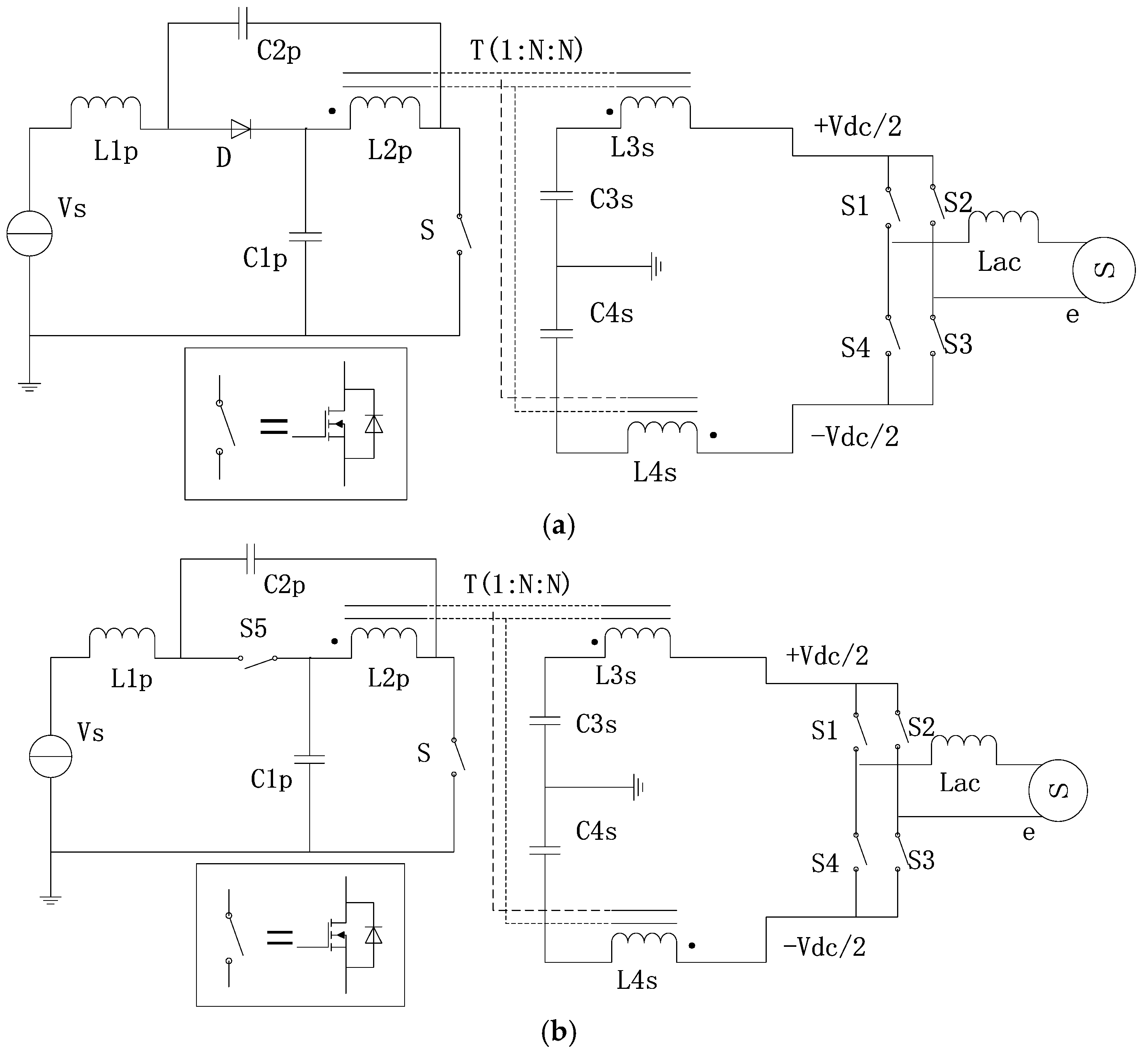
2. Circuit Topology
High-Frequency Isolated Quasi-Z-Source Inverter Design
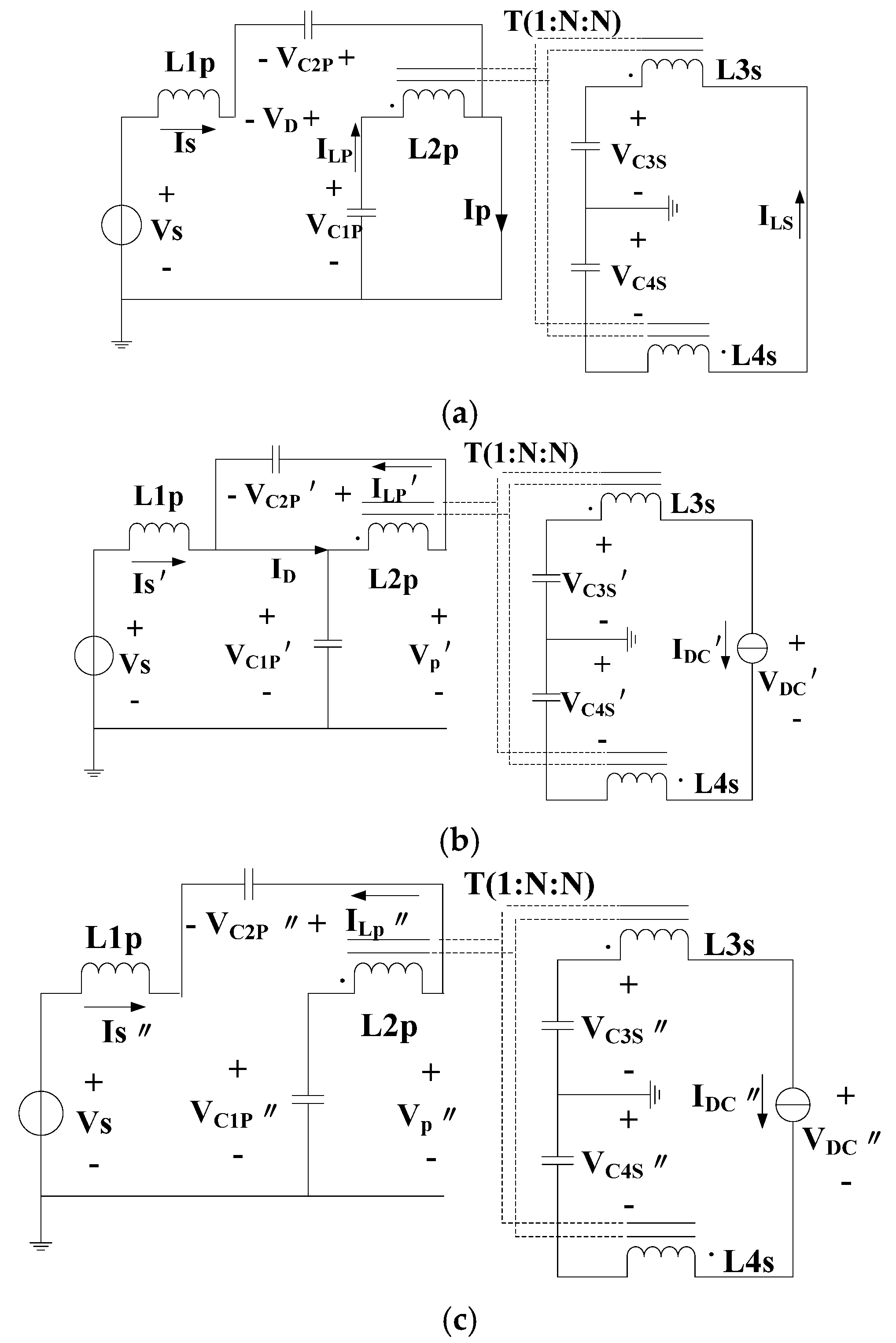
3. Modeling Analysis
3.1. Operation Principle
3.2. Abnormal Operation Conditions
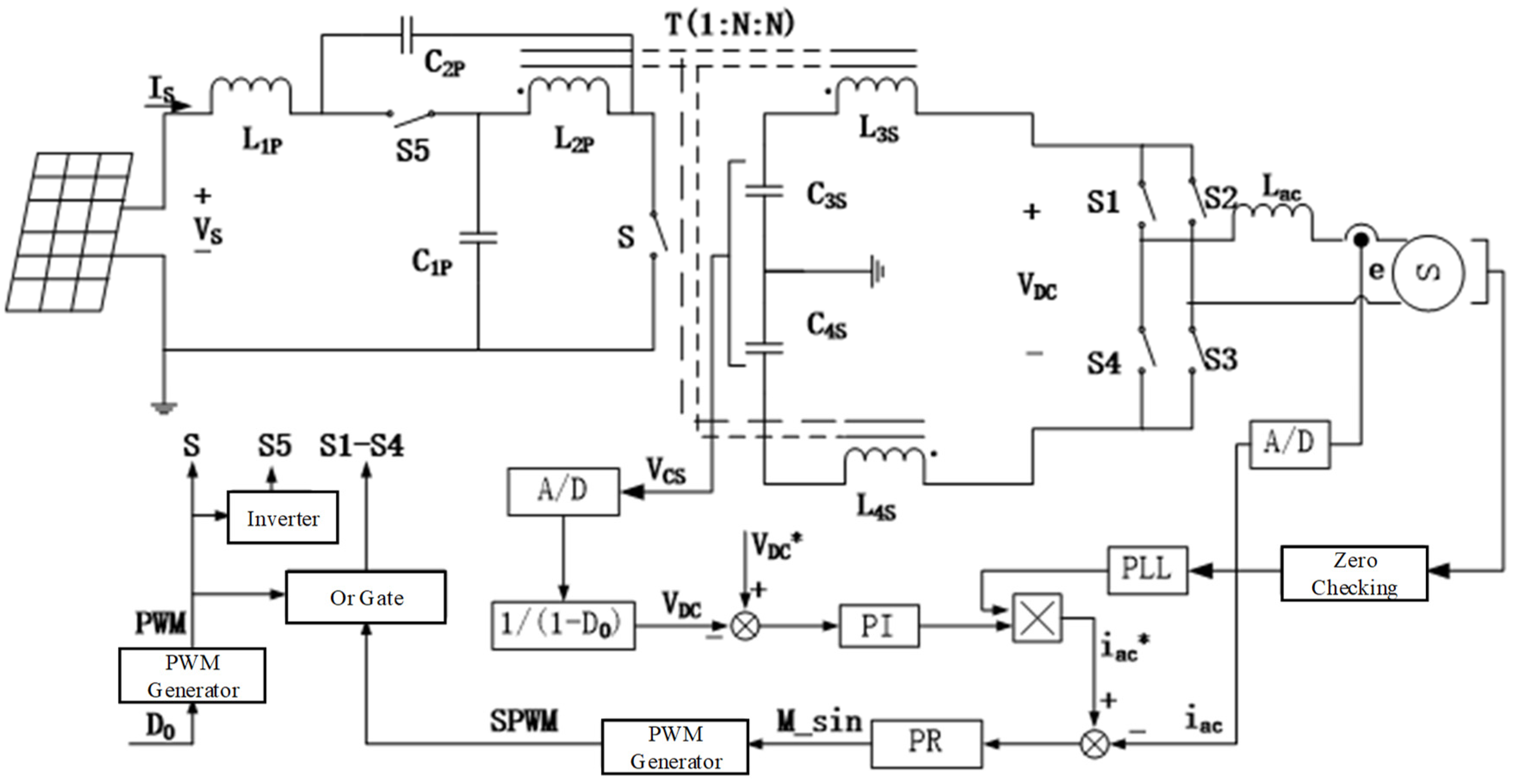
4. Control Strategy
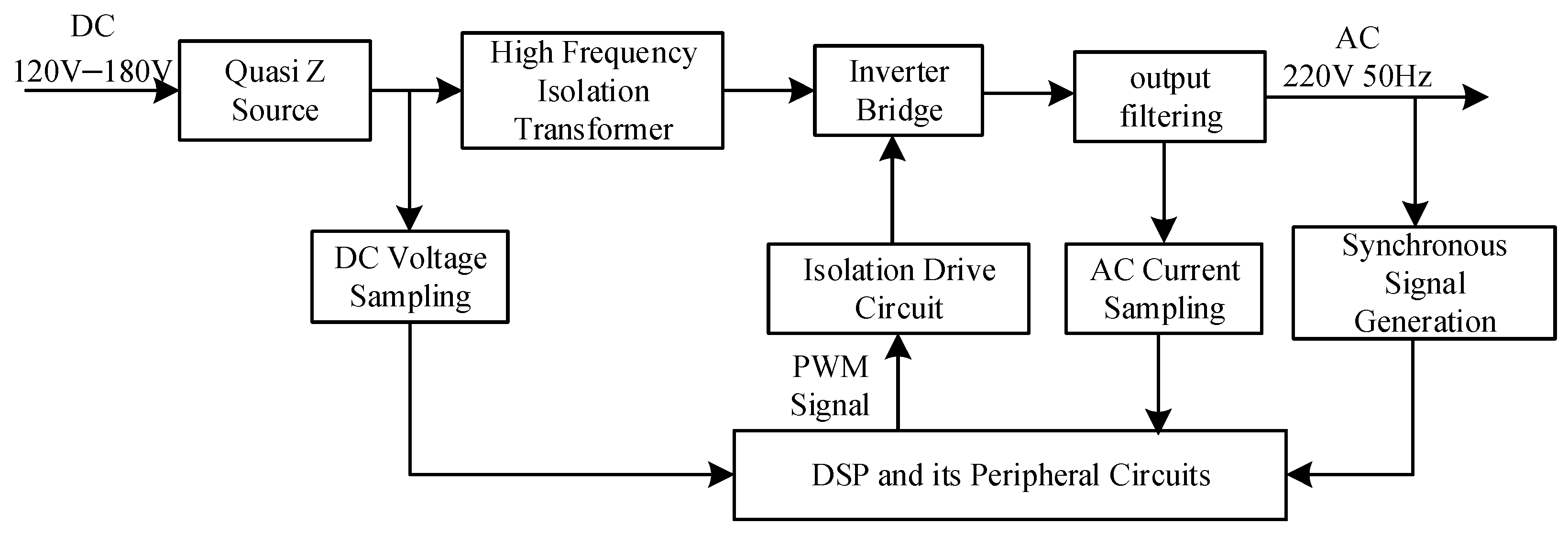
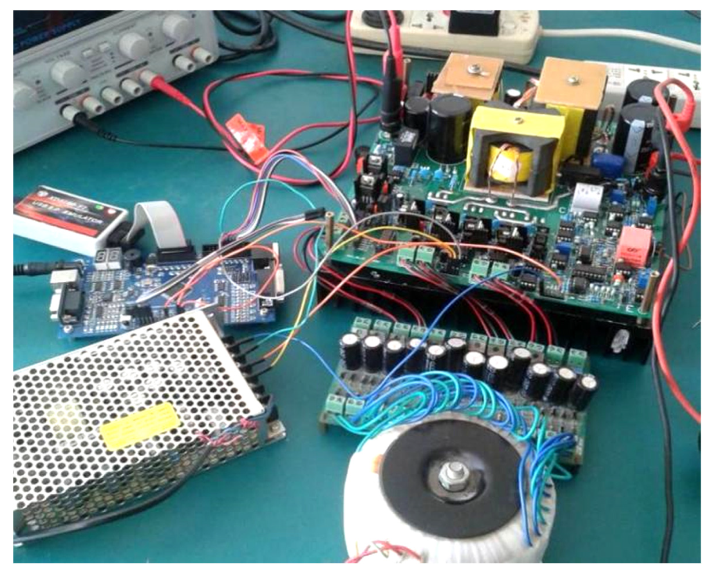
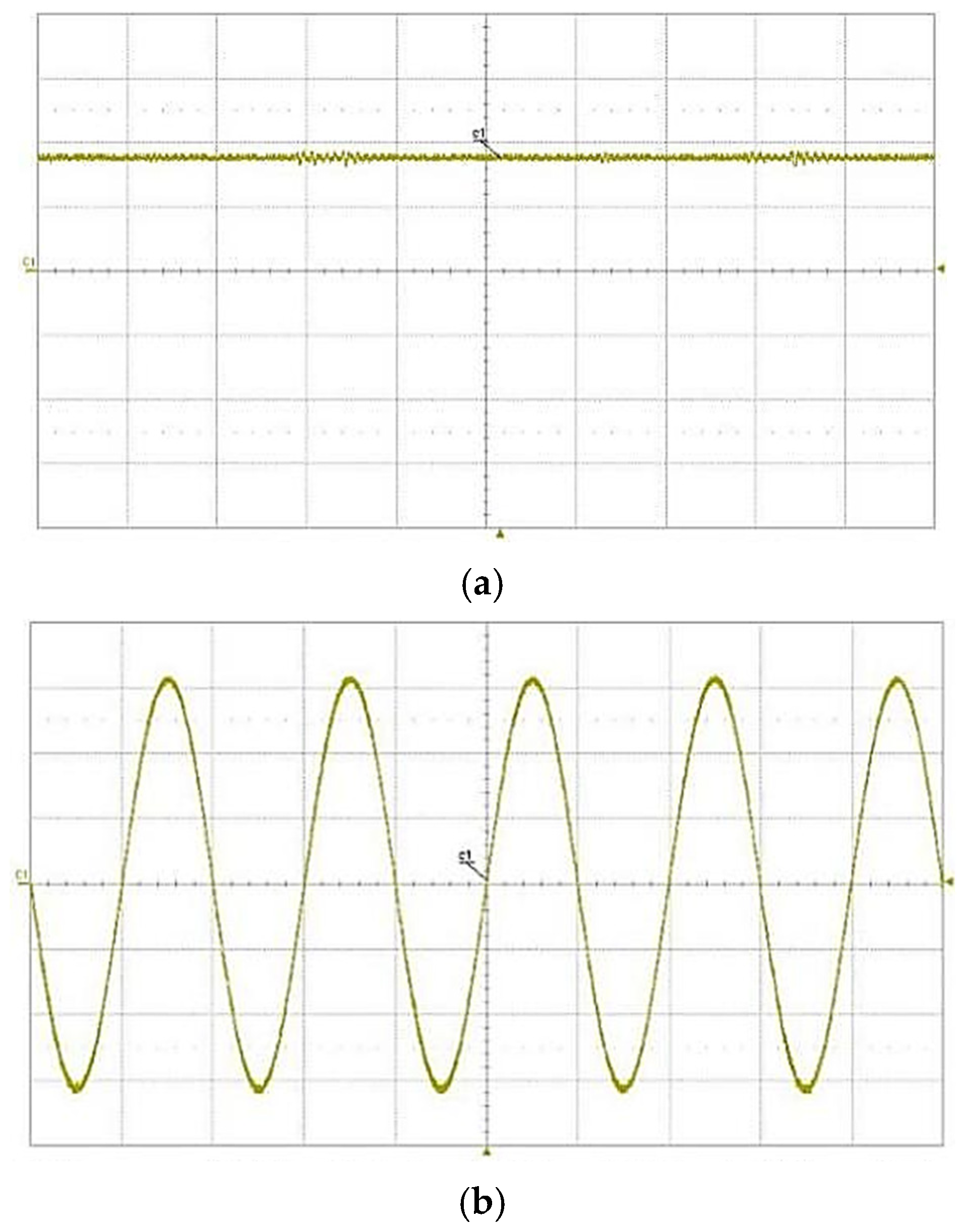
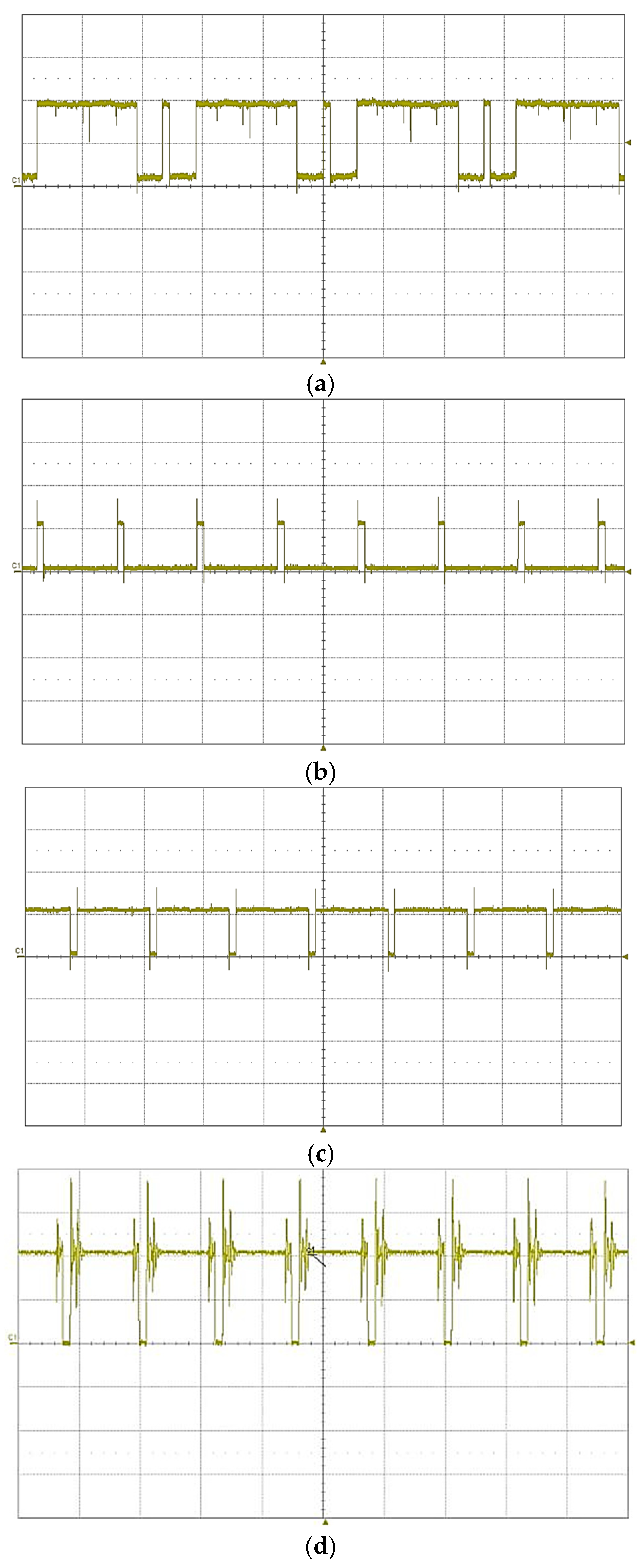
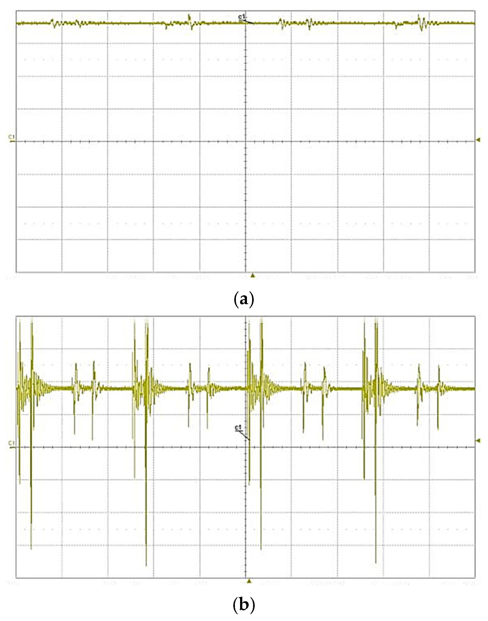
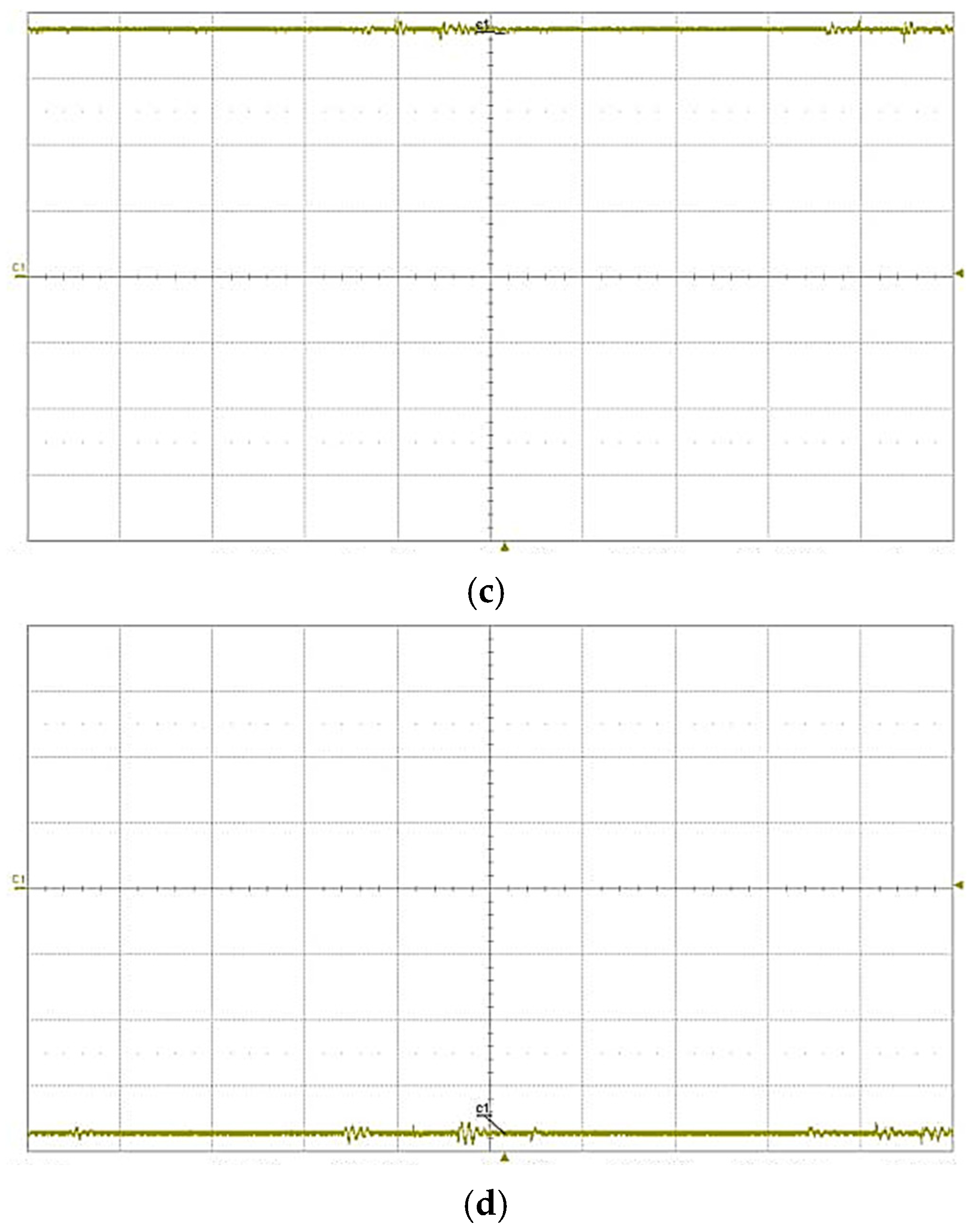
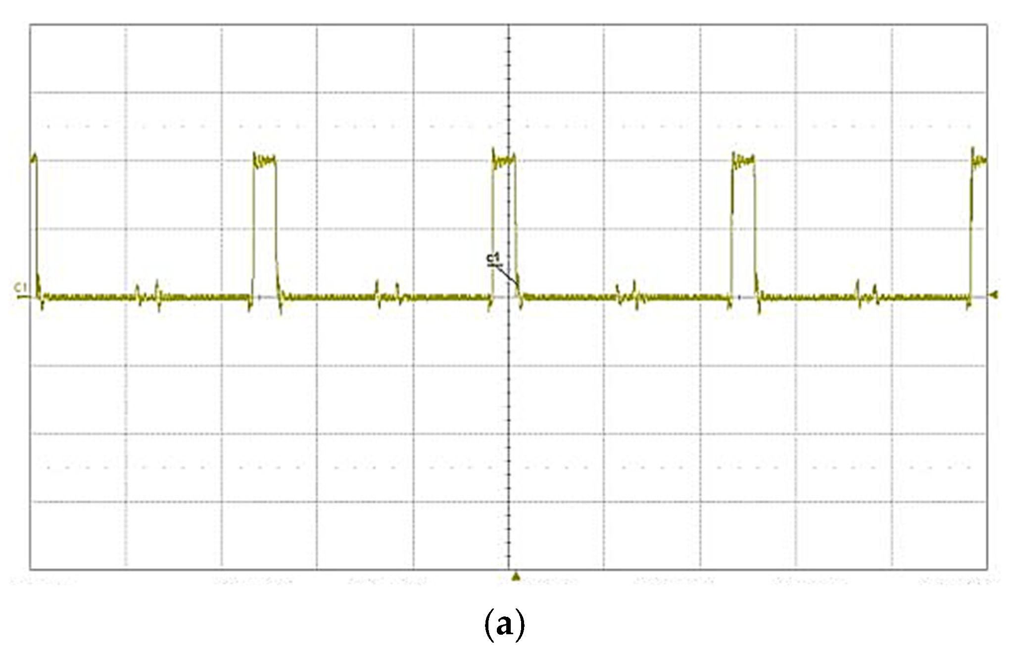
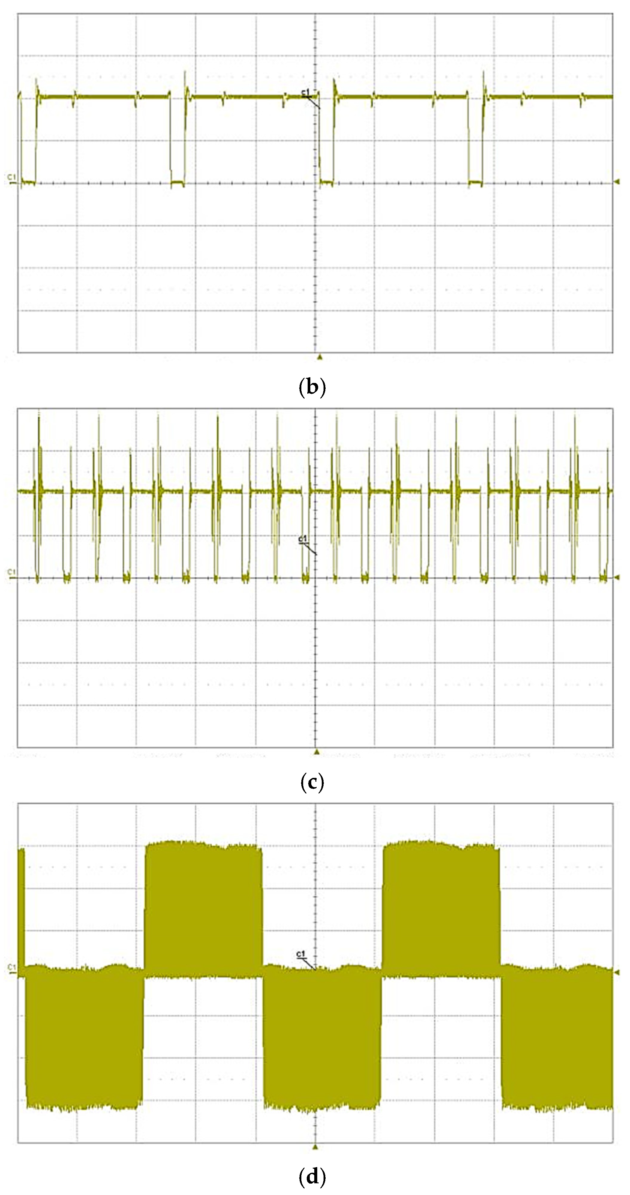
5. System Design and Experimental Verification
6. Conclusions
Author Contributions
Funding
Data Availability Statement
Conflicts of Interest
References
- Li, Y.R.; Nejabatkhah, F.; Tian, H. Smart Hybrid AC/DC Microgrids: Power Management Energy Management and Power Quality Control; Wiley: New York, NY, USA, 2022. [Google Scholar]
- Long, B.; Liao, Y.; Chong, K.T.; Rodriguez, J.; Guerrero, J.M. MPC-Controlled Virtual Synchronous Generator to Enhance Frequency and Voltage Dynamic Performance in Islanded Microgrids. IEEE Trans. Smart Grid 2021, 12, 953–964. [Google Scholar] [CrossRef]
- Liao, Y.; Wang, X. Evaluation of Voltage Regulators for Dual-Loop Control of Voltage-Controlled VSCs. In Proceedings of the 2019 IEEE Energy Conversion Congress and Exposition (ECCE), Baltimore, MD, USA, 29 September–3 October 2019; pp. 5036–5042. [Google Scholar]
- Geng, Y.; Yun, Y.; Chen, R.; Wang, K.; Bai, H.; Wu, X. Parameters Design and Optimization for LC-Type Off-Grid Inverters with Inductor-Current Feedback Active Damping. IEEE Trans. Power Electron. 2018, 33, 703–715. [Google Scholar] [CrossRef]
- Meng, X.; Liu, J.; Liu, Z. A Generalized Droop Control for Grid-Supporting Inverter Based on Comparison Between Traditional Droop Control and Virtual Synchronous Generator Control. IEEE Trans. Power Electron. 2019, 34, 5416–5438. [Google Scholar] [CrossRef]
- Dragicevic, T.; Vazquez, S.; Wheeler, P. Advanced Control Methods for Power Converters in DG Systems and Microgrids. IEEE Trans. Ind. Electron. 2021, 68, 5847–5862. [Google Scholar] [CrossRef]
- Zheng, C.; Dragicevic, T.; Blaabjerg, F. Model Predictive Control-Based Virtual Inertia Emulator for an Islanded Alternating Current Microgrid. IEEE Trans. Ind. Electron. 2021, 68, 7167–7177. [Google Scholar] [CrossRef]
- Vazquez, S.; Rodriguez, J.; Rivera, M.; Franquelo, L.G.; Norambuena, M. Model Predictive Control for Power Converters and Drives: Advances and Trends. IEEE Trans. Ind. Electron. 2017, 64, 935–947. [Google Scholar] [CrossRef]
- Zheng, C.; Dragicevic, T.; Majmunovic, B.; Blaabjerg, F. Constrained Modulated Model-Predictive Control of an LC-Filtered Voltage-Source Converter. IEEE Trans. Power Electron. 2020, 35, 1967–1977. [Google Scholar] [CrossRef]
- Karamanakos, P.; Geyer, T. Guidelines for the Design of Finite Control Set Model Predictive Controllers. IEEE Trans. Power Electron. 2020, 35, 7434–7450. [Google Scholar] [CrossRef]
- Yang, Z.; Zeng, J.; Ren, Q.; Wu, L.; Zhang, Q. A carrier-based discontinuous PWM for an 80 kw PV inverter with the reduction of the DC-link voltage ripple and common mode current. IEEE Trans. Ind. Electron. 2023, 70, 6953–6963. [Google Scholar] [CrossRef]
- Kan, S.; Ruan, X.; Huang, X. Compensation of second harmonic current based on bus voltage ripple limitation in single-phase photovoltaic grid-connected inverter. IEEE Trans. Ind. Electron. 2023, 70, 7525–7532. [Google Scholar] [CrossRef]
- Li, Z.; Cheng, Z.; Si, J.; Xu, S. Distributed Event-Triggered Hierarchical Control of PV Inverters to Provide Multi-Time Scale Frequency Response for AC Microgrid. IEEE Trans. Power Syst. 2023, 38, 1529–1542. [Google Scholar] [CrossRef]
- Chen, T.; Gu, L.; Dally, W.J.; Rivas-Davila, J.; Fox, J. A Novel High-Efficiency Three-Phase Multilevel PV Inverter with Reduced DC-Link Capacitance. IEEE Trans. Ind. Electron. 2023, 70, 4751–4761. [Google Scholar] [CrossRef]
- Ryu, T.; Choi, U.-M. Discontinuous PWM strategy for reliability and efficiency improvements of single-phase five-level T-type inverter. IEEE Trans. Ind. Electron. 2024, 71, 2567–2577. [Google Scholar] [CrossRef]
- Tak, N.; Chattopadhyay, S.K. Two-Stage Three-Phase Transformerless Hybrid Multilevel Inverter for Solar PV Application. IEEE Trans. Ind. Electron. 2024, 71, 5386–5398. [Google Scholar] [CrossRef]
- Shahabadini, M.; Moeini, N.; Bahrami-Fard, M.; Iman-Eini, H. HERIC-Based Cascaded H-Bridge Inverter for Leakage Current Suppression in PV Systems. IEEE Trans. Power Electron. 2023, 38, 4005–4014. [Google Scholar] [CrossRef]
- Wang, M.; Zhang, X.; Wu, M.; Guo, Z.; Wang, P.; Li, F. A Control Strategy for Achieving the Whole Operation Range Power Matching of Single-Phase Cascaded H-Bridge PV Inverter. IEEE Trans. Ind. Electron. 2023, 70, 5896–5906. [Google Scholar] [CrossRef]
- Lu, G.; Zhang, Q.; Zheng, D.; Mirsaeidi, S.; Zhang, P. Detection and Location Approach to Incipient Grounding Defect in Transformer Winding Based on Sequence Voltage Ratios at PV Inverter Switching Frequency. IEEE Trans. Ind. Electron. 2023, 70, 6337–6346. [Google Scholar] [CrossRef]
- Li, X.; Sun, Y.; Jiang, L.; Wang, H.; Liu, Y.; Su, M. Common-Mode Circuit Analysis of Current-Source Photovoltaic Inverter for Leakage Current and EMI. IEEE Trans. Power Electron. 2023, 38, 7156–7165. [Google Scholar] [CrossRef]
- Bountouris, P.; Tzelepis, D.; Abdulhadi, I.; Coffele, F. Dynamic Model of Commercially Available Inverters with Validation Against Hardware Testing. IEEE Trans. Power Syst. 2023, 38, 2007–2017. [Google Scholar] [CrossRef]
- Tian, H.; Chen, M.; Liang, G.; Xiao, X. A Single-Phase Transformerless Common-Ground Type PV Inverter with Active Power Decoupling. IEEE Trans. Ind. Electron. 2023, 70, 3762–3772. [Google Scholar] [CrossRef]
- Peng, F.Z. Z-Source Inverter. IEEE Trans. Ind. Appl. 2003, 39, 504–510. [Google Scholar] [CrossRef]
- Florescu, A.; Stocklosa, O.; Teodorescu, M.; Radoi, C.; Stoichescu, D.A.; Rosu, S. The advantages, limitations and disadvantages of Z-source inverter. In Proceedings of the 2010 International Semiconductor Conference (CAS 2010), Sinaia, Romania, 11–13 October 2010; pp. 483–486. [Google Scholar]
- PManoj; Kirubakaran, A.; Somasekhar, V.T. A single-stage quasi-z-source-based 5-level grid-tied PV inverter with reduced leakage curren. IEEE J. Emerg. Sel. Top. Power Electron. 2023, 11, 826–835. [Google Scholar]
- Nguyen, M.-K.; Lim, Y.-C.; Cho, G.-B. Switched-Inductor Quasi-Z-Source Inverter. IEEE Trans. Power Electron. 2011, 26, 3183–3191. [Google Scholar] [CrossRef]
- Gao, F.; Loh, P.; Li, D.; Blaabjerg, F. Asymmetrical and symmetrical embedded Z-source inverters. IET Power Electron. 2011, 4, 181–193. [Google Scholar] [CrossRef]
- Loh, P.C.; Gao, F.; Blaabjerg, F. Embedded EZ-Source Inverters. IEEE Trans. Ind. Appl. 2010, 46, 256–267. [Google Scholar]
- Vinnikov, D.; Roasto, I.; Strzelecki, R.; Adamowicz, M. Performance improvement method for the voltage-fed qZSI with continuous input current. In Proceedings of the Melecon 2010—2010 15th IEEE Mediterranean Electrotechnical Conference, Valletta, Malta, 26–28 April 2010; pp. 1459–1464. [Google Scholar]
- Qian, W.; Peng, F.Z.; Cha, H. Trans-Z-Source Inverters. IEEE Trans. Power Electron. 2011, 26, 3453–3463. [Google Scholar] [CrossRef]
- Li, D.; Loh, P.C.; Zhu, M.; Gao, F.; Blaabjerg, F. Cascaded trans-z-source inverters. In Proceedings of the ECCE Asia (ICPE 2011—ECCE Asia), Jeju, Republic of Korea, 30 May–3 June 2011; pp. 1976–1980. [Google Scholar]
- Jiang, S.; Cao, D.; Peng, F.Z. High frequency transformer isolated Z-source inverters. In Proceedings of the 2011 IEEE Applied Power Electronics Conference and Exposition—APEC 2011, Fort Worth, TX, USA, 6–11 March 2011; pp. 442–449. [Google Scholar]


| Variants | Parameters |
|---|---|
| Rated power | 500 VA |
| Input DC voltage VS | 120~180 V |
| Duty cycle Do | 0.083~0.223 |
| Grid voltage E | 220 V |
| Grid current Iac | 2.273 A |
| Capacitors C1P, C3S, C4S | 1200 μF/250 V |
| Capacitors C2P | 1200 μF/50 V |
| Parasitic resistor of capacitor R | 0.1 Ω |
| Input energy storage inductor L1P | 1.2 mH |
| Output filter inductor Lac | 5 mH |
| Parasitic resistor of inductor r | 0.1 Ω |
| Turn ratio of transformer N | 1 |
| Switching frequency f | 20 kHz |
| Control chip | TMS320F2808 |
| Phase-locked loop module | CD4046 |
| Performance Parameter | The Inverter in the Figure 1.1(a) [23] | The Inverter in the Figure 1.1(b) [25] | The Inverter in the Figure 1.1(c) [32] | The Inverter Proposed |
|---|---|---|---|---|
| The output voltage (V) | 210.00 | 212.77 | 208.00 | 220.00 |
| The peak value of the DC bus voltage (V) | 375.00 | 382.00 | 415.00 | 430.00 |
| The voltage of the capacitors | VC1P = 205.00 V, VC2P = 215.00 V | VC1P = 194.68 V, VC2P = 18.10 V | VC1P = 192.17 V, VC2P = 192.17 V, VC1S = 194.68 V, VC2S = 194.68 V | VC1P = 180.20 V, VC2P = 18.00 V, VC3S = 187.00 V, VC4S = 185.50 V |
| The voltage stress of the capacitors | High | Low | Medium | Low |
| Weight | Heavy | Light | Light | Light |
| Electrical isolation | No | Yes | High-frequency | High-frequency |
| Power flow | Uni-directional | Uni-directional | Uni-directional | Bi-directional |
| Power density | Low | Medium | High | High |
Disclaimer/Publisher’s Note: The statements, opinions and data contained in all publications are solely those of the individual author(s) and contributor(s) and not of MDPI and/or the editor(s). MDPI and/or the editor(s) disclaim responsibility for any injury to people or property resulting from any ideas, methods, instructions or products referred to in the content. |
© 2024 by the authors. Licensee MDPI, Basel, Switzerland. This article is an open access article distributed under the terms and conditions of the Creative Commons Attribution (CC BY) license (https://creativecommons.org/licenses/by/4.0/).
Share and Cite
Dong, W.; Wang, X.; Azan, D.; Wang, Y.; Li, L. Novel Quasi-Z-Source Inverter with High-Frequency AC Link of High-Proportion Renewable-Energy Power System. Processes 2024, 12, 2842. https://doi.org/10.3390/pr12122842
Dong W, Wang X, Azan D, Wang Y, Li L. Novel Quasi-Z-Source Inverter with High-Frequency AC Link of High-Proportion Renewable-Energy Power System. Processes. 2024; 12(12):2842. https://doi.org/10.3390/pr12122842
Chicago/Turabian StyleDong, Wenjuan, Xingang Wang, DeLiNuEr Azan, Yuwei Wang, and Lei Li. 2024. "Novel Quasi-Z-Source Inverter with High-Frequency AC Link of High-Proportion Renewable-Energy Power System" Processes 12, no. 12: 2842. https://doi.org/10.3390/pr12122842
APA StyleDong, W., Wang, X., Azan, D., Wang, Y., & Li, L. (2024). Novel Quasi-Z-Source Inverter with High-Frequency AC Link of High-Proportion Renewable-Energy Power System. Processes, 12(12), 2842. https://doi.org/10.3390/pr12122842