
Optimization of a Multilevel Inverter Design Used for Photovoltaic Systems under Variable Switching Controllers


Abstract
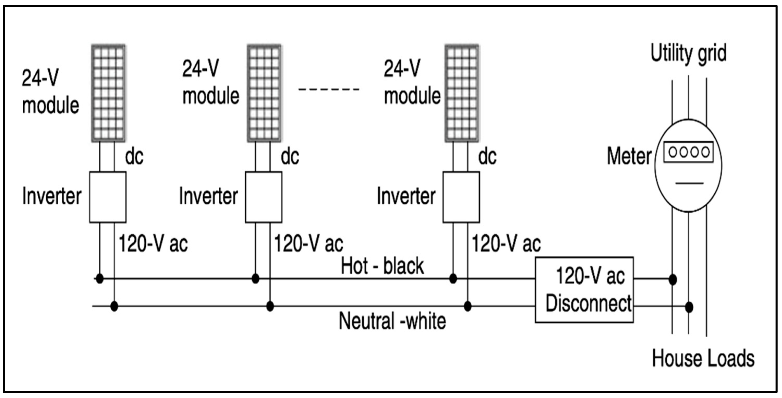
:1. Introduction
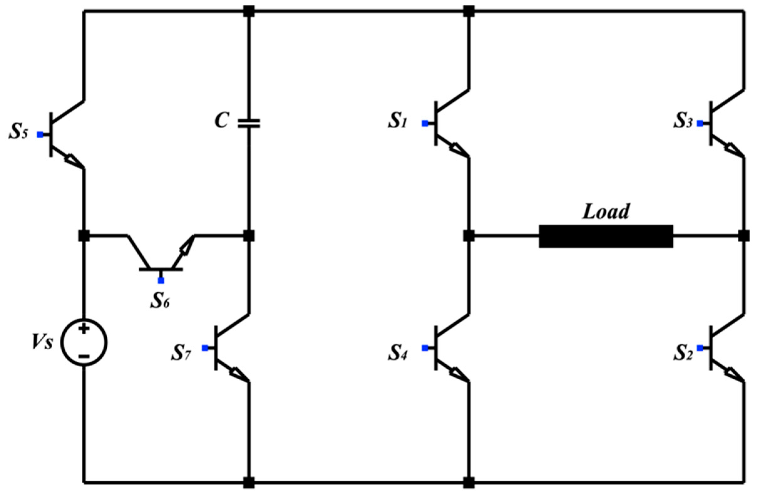
2. Proposed Topology
3. The Series to Parallel SC Cell
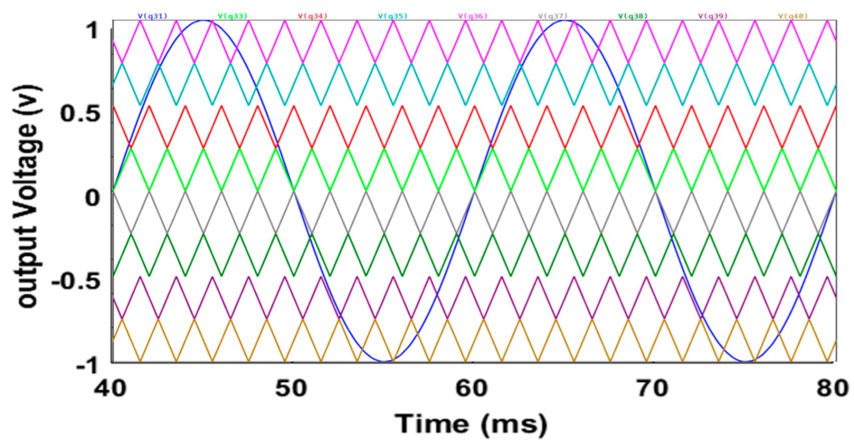
4. Control System
5. Proposed MLI Configuration
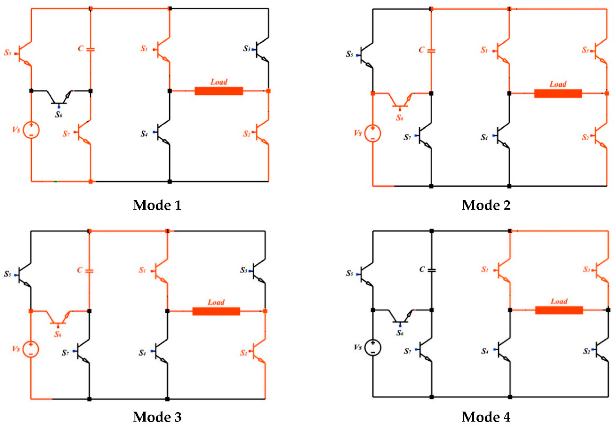
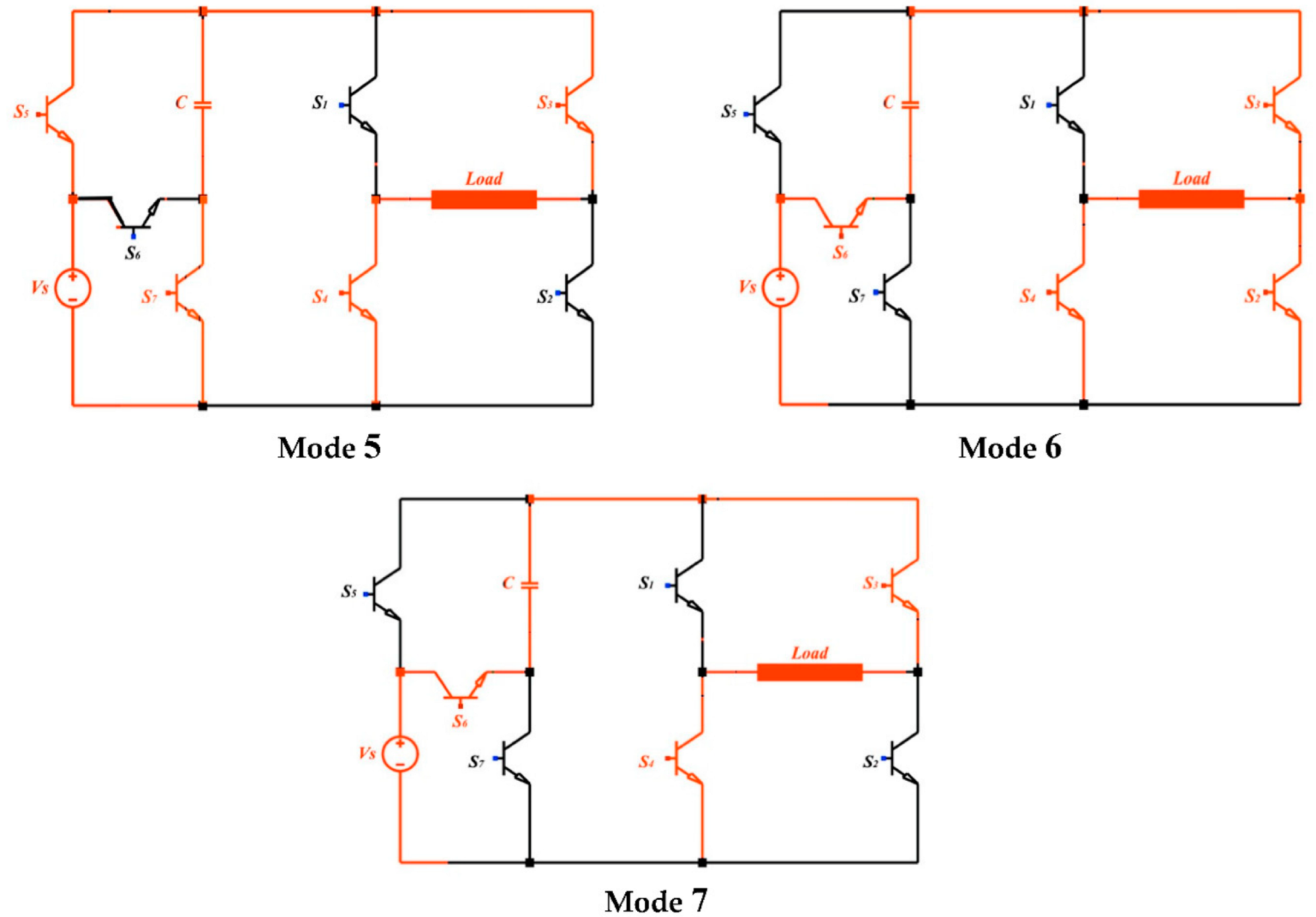
6. Modes of Operation
- Similar to the work suggested in [25], this work uses the series to parallel the configuration to achieve a 7L MLI with the least number of input sources and switches.
- The work in [25] used three input sources to implement the 7L inverter; however, this work used only a single input source with an SC cell. 3.The single input source used in this work is connected to an H-bridge inverter through an SC cell operating in the series to parallel; thus, the SC cell behaves as an additional input source.
- From a practical point of view, the switching states of the switches of the H-bridge can be obtained using the method suggested in [20].
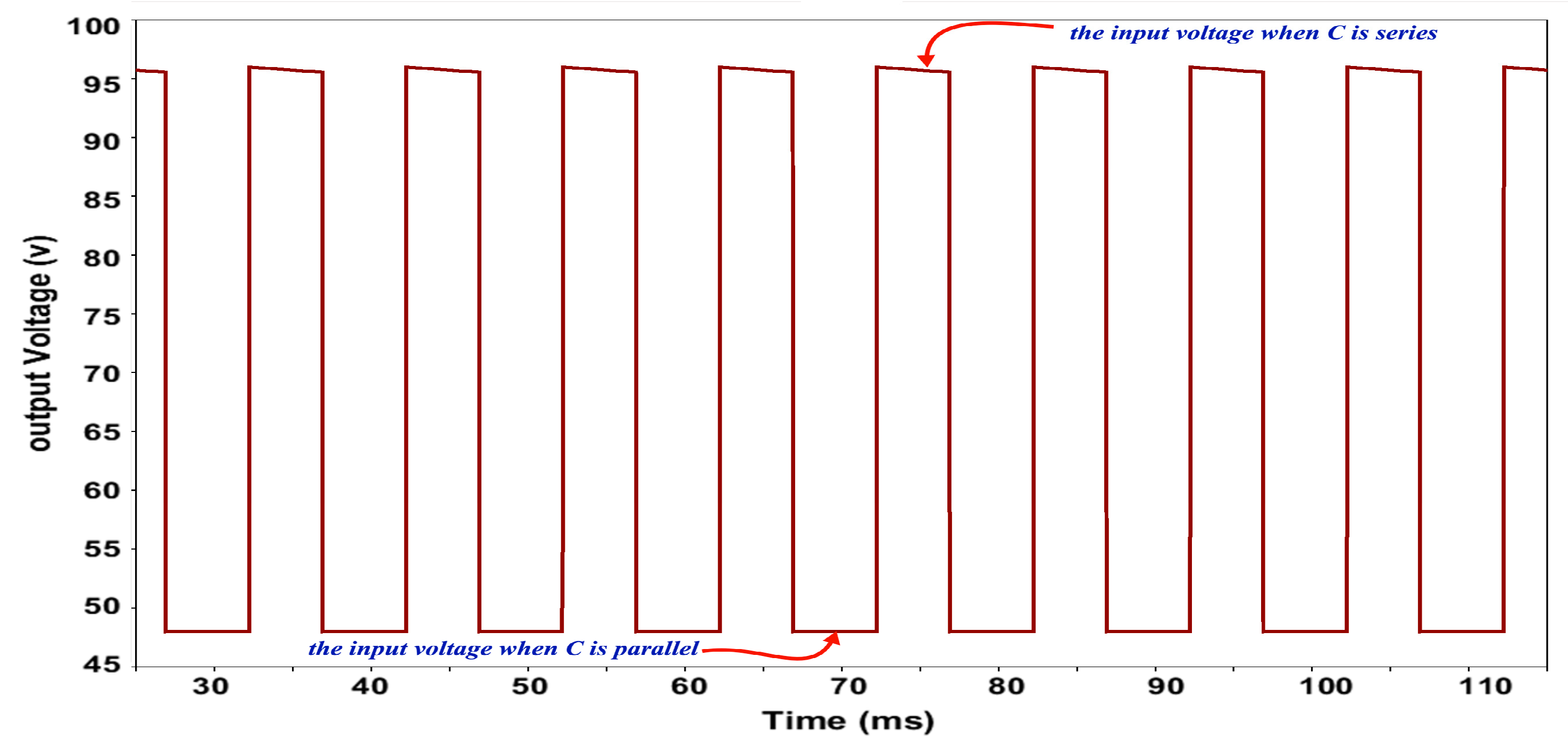
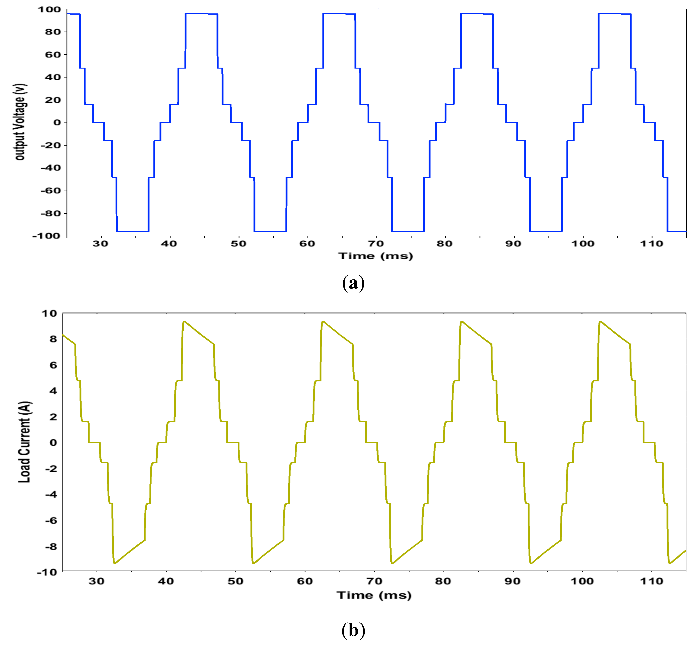
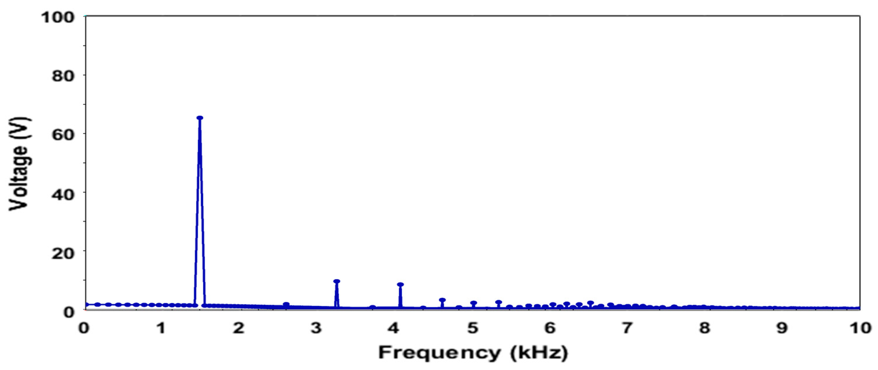
7. Results and Discussion
8. Conclusions
Author Contributions
Funding
Acknowledgments
Conflicts of Interest
References
- Alateeq, A.S.; Almalaq, Y.A.; Matin, M.A. Modeling and simulation of GaN step-up power switched capacitor converter. In Proceedings of the SPIE 10381, Wide Bandgap Power Devices and Applications II, San Diego, CA, USA, 6–10 August 2017. [Google Scholar]
- Alateeq, A.S.; Almalaq, Y.A.; Matin, M.A. A Performance of the Soft Charging Operation in Series of Step-Up Power Switched-Capacitor Converters. J. Low Power Electron. Appl. 2018, 8, 8. [Google Scholar] [CrossRef] [Green Version]
- Alateeq, A.S.; Almalaq, Y.A.; Matin, M.A. A switched-inductor model for a non-isolated multilevel boost converter. In Proceedings of the 2017 North American Power Symposium (NAPS), Morgantown, WV, USA, 17–19 September 2017; p. 15. [Google Scholar]
- Sagar, M.; Ranjana, B. A Novel Non-Isolated Switched Inductor Floating Output DC-DC Multilevel Boost Converter For Fuelcell Applications. In Proceedings of the 2014 IEEE Students’ Conference on Electrical, Electronics and Computer Science, Bhopal, India, 1–2 March 2014; p. 14254943. [Google Scholar]
- Du, Z.; Tolbert, L.M.; Chiasson, J.N.; Ozpineci, B. Reduced Switching-Frequency Active Harmonic Elimination for Multilevel Converters. IEEE Trans. Power Electron. 2008, 55, 1761–1770. [Google Scholar]
- Ebrahimi, J.; Babaei, E.; Gharehpetian, G.B. A new topology of cascaded multilevel converters with reduced number of components for high-voltage applications. IEEE Trans. Power Electron. 2011, 26, 3109–3118. [Google Scholar] [CrossRef]
- Alateeq, A.; Matin, M. A Novel Design of a High Gain Step-up Converter Using Switched-Capacitors/Switched-Inductors Cells. In Proceedings of the 2018 IEEE International Conference on Electro Information Technology (EIT), Rochester, MI, USA, 3–5 May 2018. (In the Press). [Google Scholar]
- Lai, J.S.; Peng, F.Z. Multilevel converters—A new breed of power converters. IEEE Trans. Ind. Applicat. 1996, 32, 509–517. [Google Scholar]
- Babaei, E.; Laali, S.; Bayat, Z. A single-phase cascaded multilevel inverter based on a new basic unit with reduced number of power switches. IEEE Trans. Ind. Electron. 2014, 62, 922–929. [Google Scholar] [CrossRef]
- Arbune, P.A.; Gaikwad, A. Comparative Study of Three level and five level Inverter. Int. J. Adv. Res. Electr. Electron. Instrum. Eng. 2016, 5, 681–686. [Google Scholar]
- Rodriguez, J.; Lai, J.S.; Peng, F.Z. Multilevel inverters: A survey of topologies controls and applications. IEEE Trans. Ind. Electron. 2002, 49, 724–738. [Google Scholar] [CrossRef] [Green Version]
- Manjrekar, M.D.; Lipo, T.A. A hybrid multilevel inverter topology for drive applications. In Proceedings of the IEEE APEC’98 Thirteenth Annual Applied Power Electronics Conference and Exposition, Anaheim, CA, USA, 15–19 February 1998; pp. 523–529. [Google Scholar]
- Hammond, P. A new approach to enhance power quality for medium voltage ac drives. IEEE Trans. Ind. Applicat. 1997, 33, 202–208. [Google Scholar] [CrossRef]
- Meynard, T.A.; Foch, H. Multi-level choppers for high voltage applications. Eur. Power Electron. Drives J. 1992, 2, 41. [Google Scholar] [CrossRef]
- Hochgraf, C.; Lasseter, R.; Divan, D.; Lipo, T.A. Comparison of multilevel inverters for static var compensation. In Proceedings of the 1994 IEEE Industry Applications Society Annual Meeting, Denver, CO, USA, 2–6 October 1994; pp. 921–928. [Google Scholar]
- Tolbert, L.; Peng, F.Z.; Habetler, T. Multilevel converter for large electrical drives. IEEE Trans. Ind. Applicat. 1999, 35, 36–44. [Google Scholar] [CrossRef] [Green Version]
- Cao, W.; Xu, Y.; Han, Y.; Ren, B. Comparison of cascaded multilevel and modular multilevel converters with energy storage system. In Proceedings of the 2016 IEEE 11th Conference on Industrial Electronics and Applications (ICIEA), Hefei, China, 5–7 June 2016; pp. 290–294. [Google Scholar]
- Uddin, M.J.; Islam, M.S. Implementation of Cascaded Multilevel Inverter with Reduced Number of Components. In Proceedings of the 2021 2nd International Conference on Robotics, Electrical and Signal Processing Techniques (ICREST), Dhaka, Bangladesh, 5–7 January 2021; pp. 669–672. [Google Scholar] [CrossRef]
- Nabae, A.; Takahashi, I.; Akagi, H. A new neutral-point clamped PWM inverter. IEEE Trans. Ind. Applicat. 1981, IA-17, 518–523. [Google Scholar] [CrossRef]
- Pharne, I.D.; Bhosale, Y.N. A review on multilevel inverter topology. In Proceedings of the IEEE International Conference on Power Energy and Control (ICPEC), Dindigul, India, 6–8 February 2013; pp. 700–703. [Google Scholar]
- Najafi, E.; Yatim, A.H. Design and implementation of a new multilevel inverter topology. IEEE Trans. Ind. Electron. 2011, 59, 4148–4154. [Google Scholar] [CrossRef]
- Nedumgatt, J.J.; Kumar, D.V.; Kirubakaran, A.; Umashankar, A.S. Multilevel inverter with reduced number of switches. In Proceedings of the 2012 IEEE Students’ Conference on Electrical Electronics and Computer Science, Kollam, India, 20–21 April 2017; pp. 1–4. [Google Scholar]
- Manjrekar, M.; Venkataramanan, G. Advanced topologies and modulation strategies for multilevel inverters. In Proceedings of the PESC Record. 27th Annual IEEE Power Electronics Specialists Conference, Baveno, Italy, 23–27 June 1996; pp. 1013–1018. [Google Scholar]
- Ramani, K.; Sathik, M.A.; Sivakumar, S. A New Symmetric Multilevel Inverter Topology Using Single and Double Source Sub-Multilevel Inverters. J. Power Electron. 2015, 15, 96–105. [Google Scholar] [CrossRef] [Green Version]
- Motaparthiand, N.; Malligunta, K. Seven-Level Symmetrical Series/Parallel Multilevel Inverter with PWM Technique Using Digital Logic. Int. J. Electr. Comput. Eng. Syst. 2021, 12, 123–130. [Google Scholar]
- Buticchi, G.; Lorenzani, E.; Franceschini, G. A five level single-phase grid-connected converter for renewable distributed systems. IEEE Trans. Ind. Electron. 2013, 60, 906–918. [Google Scholar] [CrossRef]
- Myrzik, J.M.A. Novel inverter topologies for single-phase stand-alone or grid-connected photovoltaic systems. In Proceedings of the 4th IEEE International Conference on Power Electronics and Drive Systems, Denpasar, Indonesia, 25–25 October 2001; pp. 103–108. [Google Scholar]
- Wang, Y.; Li, Y.; Cao, Y.; Tan, Y.; He, L.; Han, J. Hybrid AC/DC microgrid architecture with comprehensive control strategy for energy management of smart building. Int. J. Electr. Power Energy Syst. 2018, 101, 151–161. [Google Scholar] [CrossRef]
- Panagis, P.; Stergiopoulos, F.; Marabeas, P.; Manias, S. Comparison of State of the Art Multilevel Inverters. In Proceedings of the IEEE Power Electronics Specialists Conference, Rhodes, Greece, 15–19 June 2008; pp. 4296–4301. [Google Scholar]
- Górecki, K.; Dąbrowski, J.; Krac, E. SPICE-Aided Modeling of Daily and Seasonal Changes in Properties of the Actual Photovoltaic Installation. Energies 2021, 14, 6247. [Google Scholar] [CrossRef]
- Piccini, A.R.; Guimarães, G.C.; de Souza, A.C.; Denardi, A.M. Implementation of a Photovoltaic Inverter with Modified Automatic Voltage Regulator Control Designed to Mitigate Momentary Voltage Dip. Energies 2021, 14, 6244. [Google Scholar] [CrossRef]
- Masters, G.M. Renewable and Efficient Electric Power Systems. John Wiley & Sons Inc.: Hoboken, NJ, USA, 2004. [Google Scholar]
- Seeman, M.D.; Sanders, S.R. Analysis and Optimization of Switched-Capacitor DC-DC Converters. IEEE Trans. Power Electron. 2008, 23, 841–851. [Google Scholar] [CrossRef]
- Alateeq, A.; Almalaq, Y.; Matin, M. Using SiC MOSFET in switched-capacitor converter for high voltage applications. In Proceedings of the 2016 North American Power Symposium (NAPS), Denver, CO, USA, 18–20 September 2016; pp. 1–5. [Google Scholar]
- Xiong, S.; Wong, S.C.; Tan, S.C.; Tse, C.K. A Family of Exponential Step-Down Switched-Capacitor Converters and Their Applications in Two-Stage Converters. IEEE Trans. Power Electron. 2014, 29, 1870–1880. [Google Scholar] [CrossRef] [Green Version]
- Baddipadiga, B.P.; Ferdowsi, M. A High-Voltage-Gain DC-DC Converter Based on Modified Dickson Charge Pump Voltage Multiplier. IEEE Trans. Power Electron. 2017, 32, 7707–7715. [Google Scholar] [CrossRef]
- Ayudhya, R.S.N. A switched-capacitor Dickson charge pumps for high-voltage high power applications. In Proceedings of the 2014 International Conference on Information Science, Electronics and Electrical Engineering, Sapporo, Japan, 26–28 April 2014; pp. 1147–1150. [Google Scholar]
- Abraham, C.; Jose, B.R.; Mathew, J.; Evzelman, M. Modelling, simulation and experimental investigation of a new two input, series-parallel switched capacitor converter. IET Power Electron. 2017, 10, 368–376. [Google Scholar] [CrossRef]
- Pérez-Nicoli, P.; Lisboa, P.C.; Veirano, F.; Silveira, F. A series–parallel switched capacitor step-up DC–DC converter and its gate-control circuits for over the supply rail switches. Analog Integr. Circuits Signal Process. 2015, 85, 37–45. [Google Scholar] [CrossRef]
- Dias, J.C.; Lazzarin, T.B. Steady State Analysis of Voltage Multiplier Ladder switched-capacitor cell. In Proceedings of the 2016 12th IEEE International Conference on Industry Applications (INDUSCON), Curitiba, PR, Brazil, 20–23 November 2016. [Google Scholar]
- Babaei, E.; Hosseini, S.H.; Gharehpetian, G.B.; Haque, M.T.; Sabahi, M. Reduction of dc voltage sources and switches in asymmetrical multilevel converters using a novel topology. Electr. Power Syst. Res. 2007, 77, 1073–1085. [Google Scholar] [CrossRef]
- Jayabalan, M.; Jeevarathinam, B.; Sandirasegarane, T. Reduced switch count pulse width modulated multilevel inverter. IET Power Electron. 2017, 10, 10–17. [Google Scholar] [CrossRef]
- Thiyagarajan, V.; Somasundaram, P. A New Seven Level Symmetrical Inverter with Reduced Switch Count. Int. J. Power Electron. Drive Syst. 2018, 9, 921–925. [Google Scholar]
- Barah, S.S.; Behera, S. An Optimize Configuration of H-Bridge Multilevel Inverter. In Proceedings of the 2021 1st International Conference on Power Electronics and Energy (ICPEE), Bhubaneswar, India, 2–3 January 2021; pp. 1–4. [Google Scholar]
- Inverter, Solar Inverter, Home Power Inverter. Available online: https://www.inverter.com/ (accessed on 24 May 2022).


| Output Voltage Level | S1 | S2 | S3 | S4 | S5 | S6 | S7 | C1 |
|---|---|---|---|---|---|---|---|---|
| +2Vin. | 1 | 1 | 0 | 0 | 0 | 1 | 0 | D |
| +1.75Vin. | 1 | 1 | 1 | 0 | 0 | 1 | 0 | D |
| +1Vin. | 1 | 1 | 0 | 0 | 1 | 0 | 1 | C |
| 0 | 1 | 1 | 0 | 0 | 0 | 0 | 0 | - |
| −1Vin. | 0 | 0 | 1 | 1 | 1 | 0 | 1 | C |
| −1.75Vin. | 0 | 1 | 1 | 1 | 0 | 1 | 0 | D |
| −2Vin. | 0 | 0 | 1 | 1 | 0 | 1 | 0 | D |
Publisher’s Note: MDPI stays neutral with regard to jurisdictional claims in published maps and institutional affiliations. |
© 2022 by the authors. Licensee MDPI, Basel, Switzerland. This article is an open access article distributed under the terms and conditions of the Creative Commons Attribution (CC BY) license (https://creativecommons.org/licenses/by/4.0/).
Share and Cite
Alateeq, A.; Almalaq, Y.; Alateeq, A. Optimization of a Multilevel Inverter Design Used for Photovoltaic Systems under Variable Switching Controllers. Processes 2022, 10, 1159. https://doi.org/10.3390/pr10061159
Alateeq A, Almalaq Y, Alateeq A. Optimization of a Multilevel Inverter Design Used for Photovoltaic Systems under Variable Switching Controllers. Processes. 2022; 10(6):1159. https://doi.org/10.3390/pr10061159
Chicago/Turabian StyleAlateeq, Ayoob, Yasser Almalaq, and Abdulaziz Alateeq. 2022. "Optimization of a Multilevel Inverter Design Used for Photovoltaic Systems under Variable Switching Controllers" Processes 10, no. 6: 1159. https://doi.org/10.3390/pr10061159
APA StyleAlateeq, A., Almalaq, Y., & Alateeq, A. (2022). Optimization of a Multilevel Inverter Design Used for Photovoltaic Systems under Variable Switching Controllers. Processes, 10(6), 1159. https://doi.org/10.3390/pr10061159