
Analysis and Implementation of a Bidirectional Converter with Soft Switching Operation

Abstract
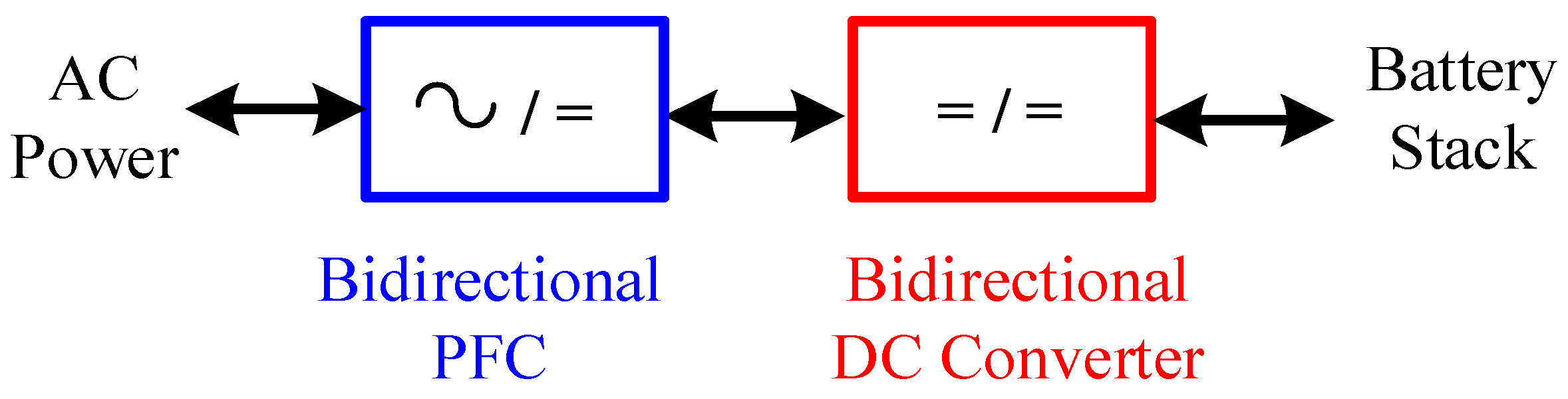
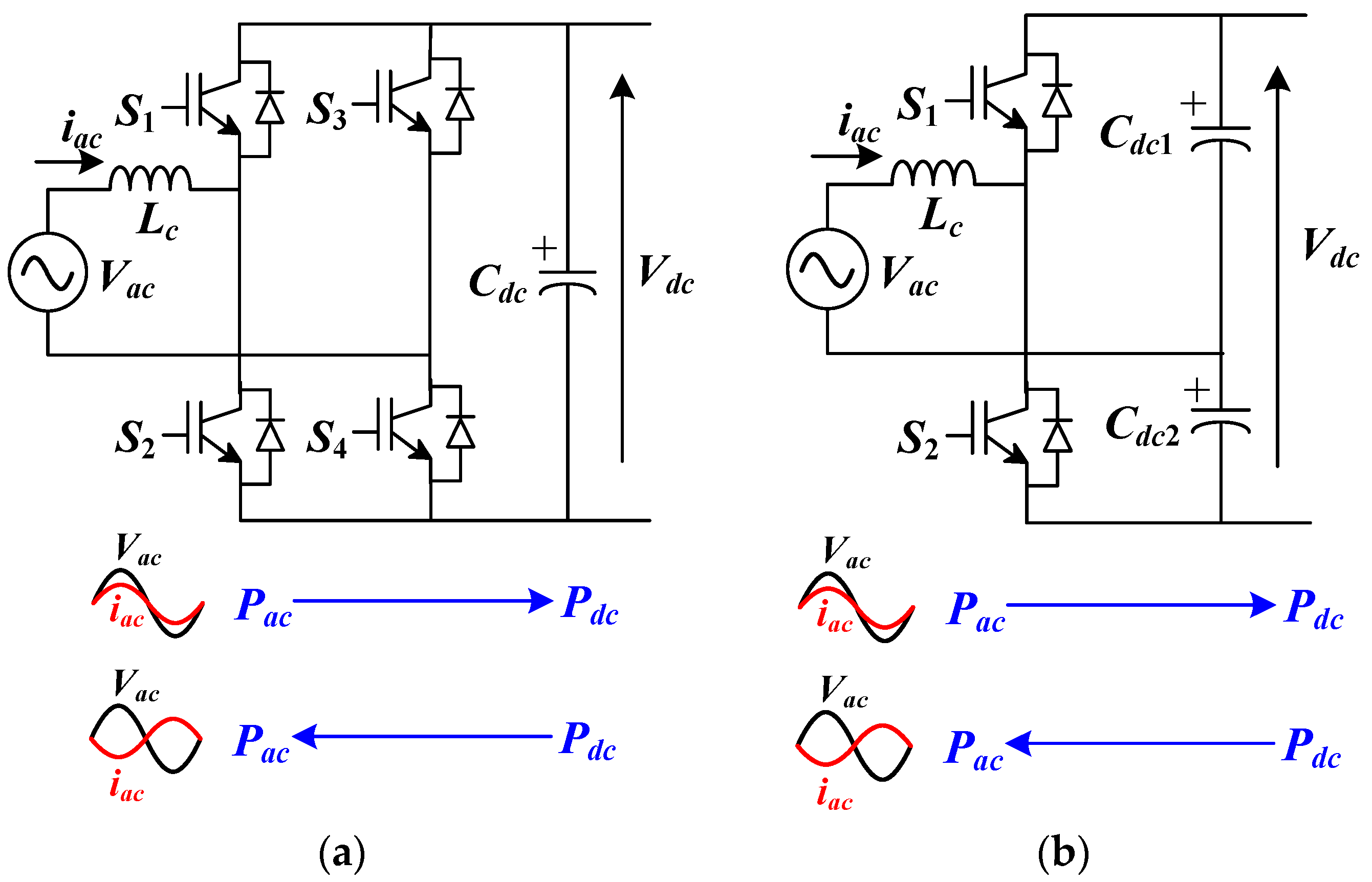
:1. Introduction
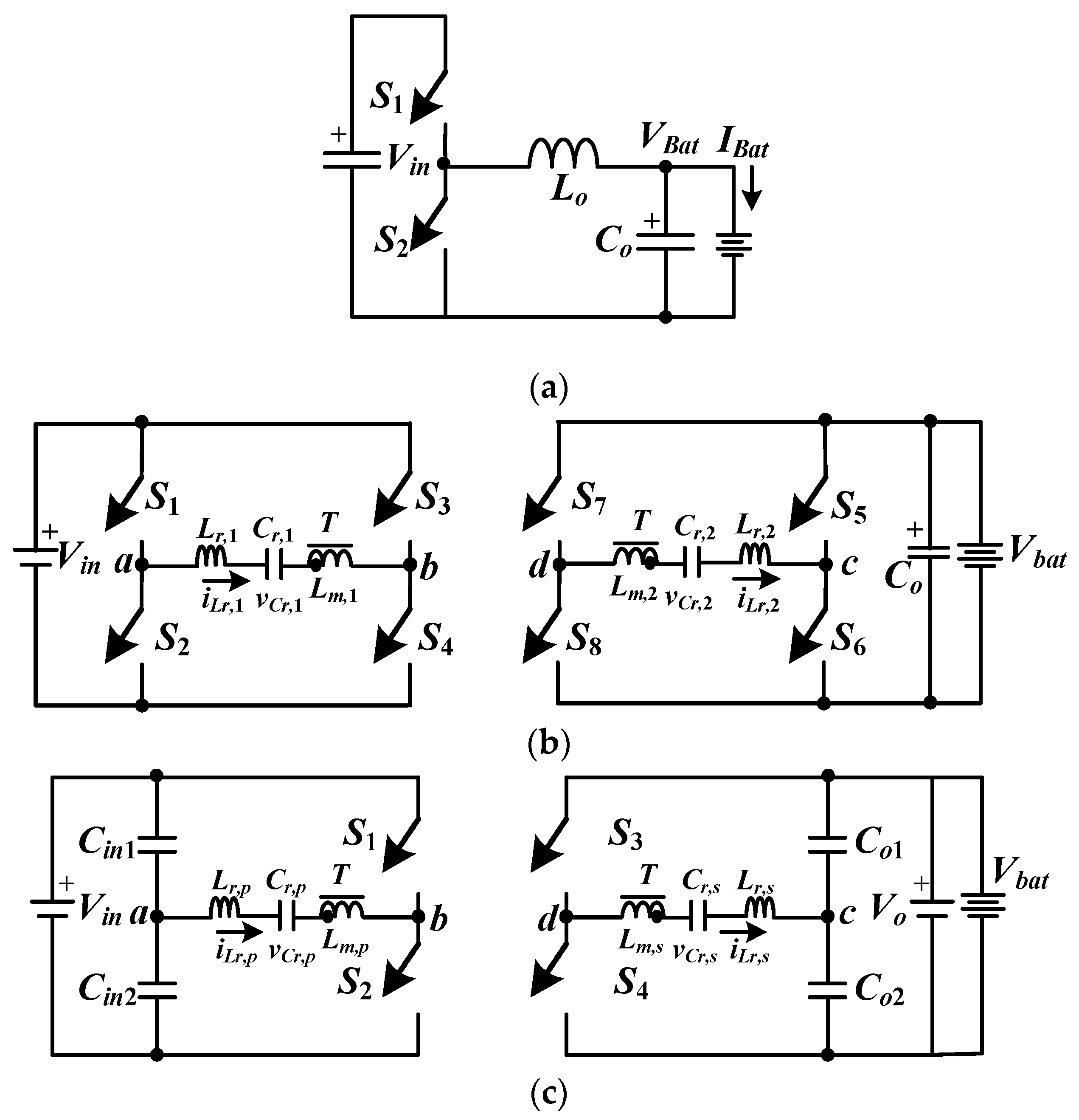
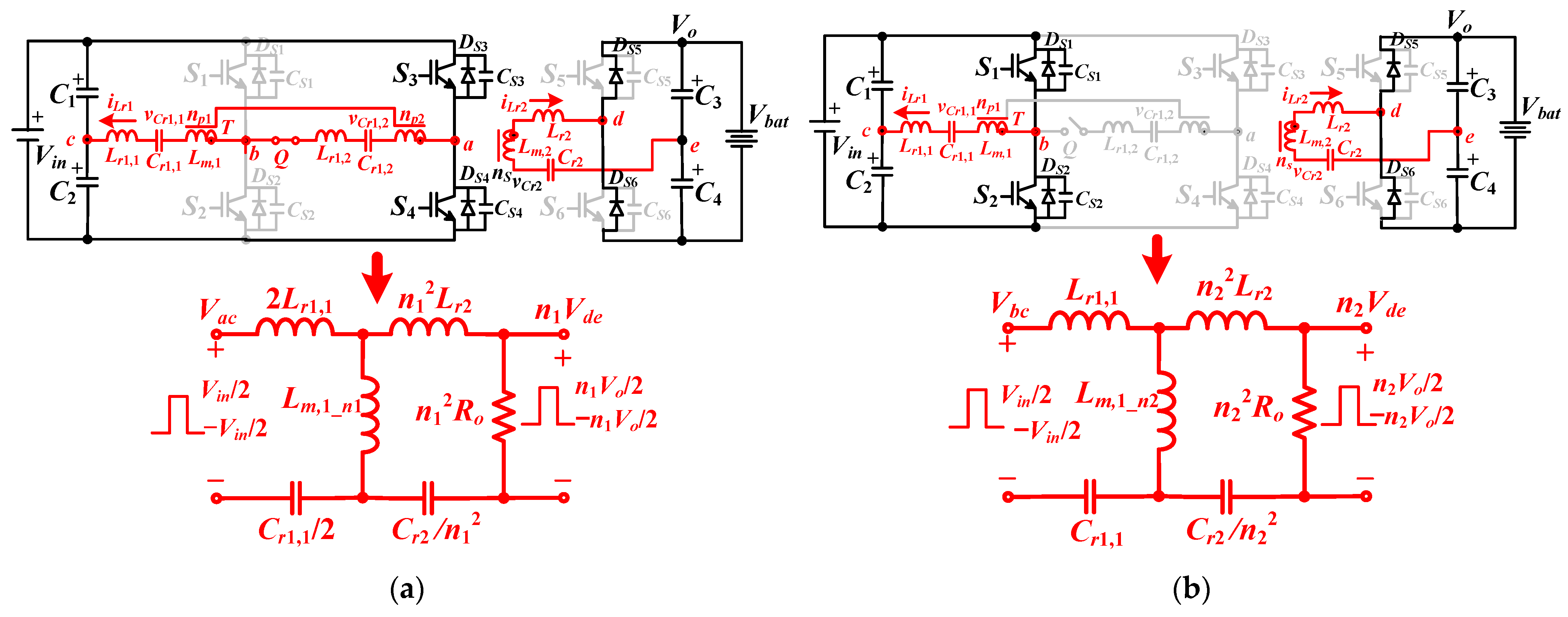
2. Circuit Diagram and the Principle of Operation
2.1. Forward Power Conversion and Low Voltage Output
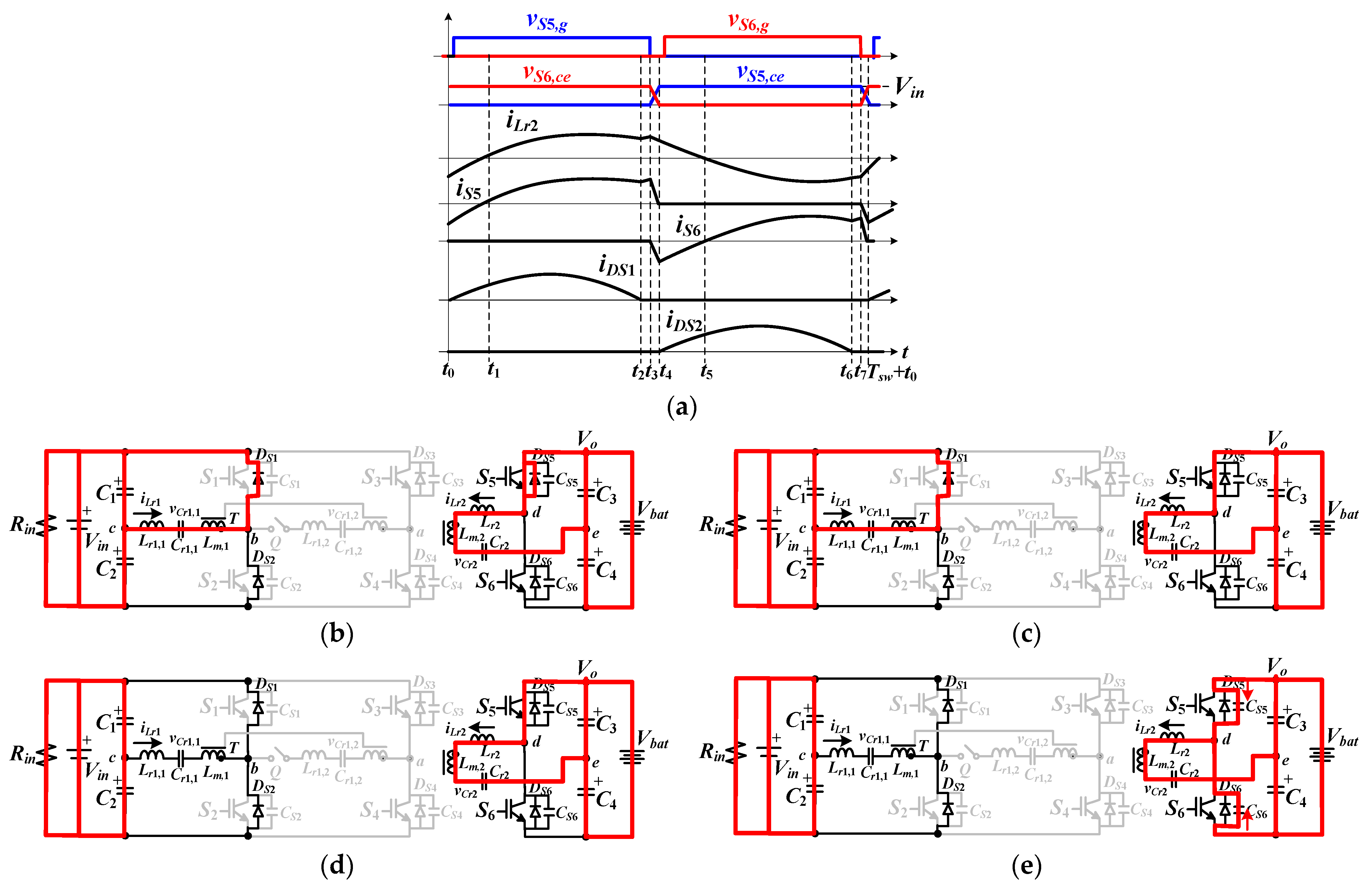
- State 1
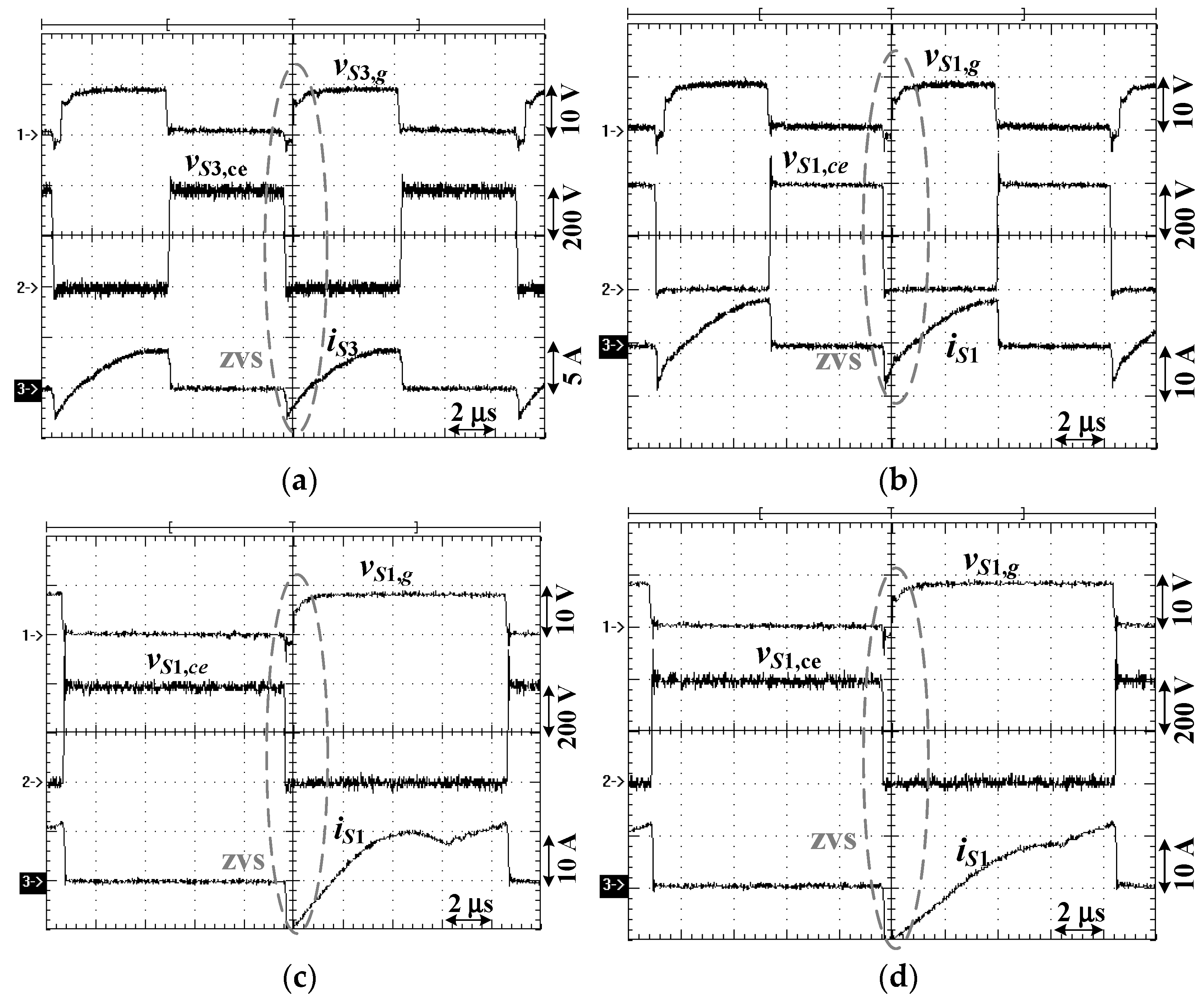
- [t0 ≤ t < t1]: For t = t0, the output capacitor voltage vCS3 is decreased to zero voltage and the diode DS3 becomes forward biased, owing to iLr1(t0) being negative. At this time, S1 is turned on, to have zero voltage switching. Since iLr2 is positive, the antipallel diodes DS5 and DS6 are conducting.
- State 2
- [t1 ≤ t < t2]: The primary current iLr1 becomes positive value after t1. Therefore, iLr1 will flow through switch S3 instead of diode DS3. In this state, the forward power flow is from C1 to C3. The leg voltages are Vac = VC1 = Vin/2 and Vde = VC3 = Vo/2. The series resonant frequency is . If fsw < (or >) fr, then the next state operation of the proposed circuit will go to state 3 (or state 4).
- State 3
- [t2 ≤ t < t3]: At time t2, iLr2 becomes zero at time t2 and DS5 becomes off. iLr1 flows through S3, Lm,1, Cr1,1, Lr1,1, Cr1,2, Lr1,2, and C1.
- State 4
- [t3 ≤ t < t4]: At time t3, S3 turns off. iLr1 charges CS3 and discharges CS4. VCS4 = 0 at t4.
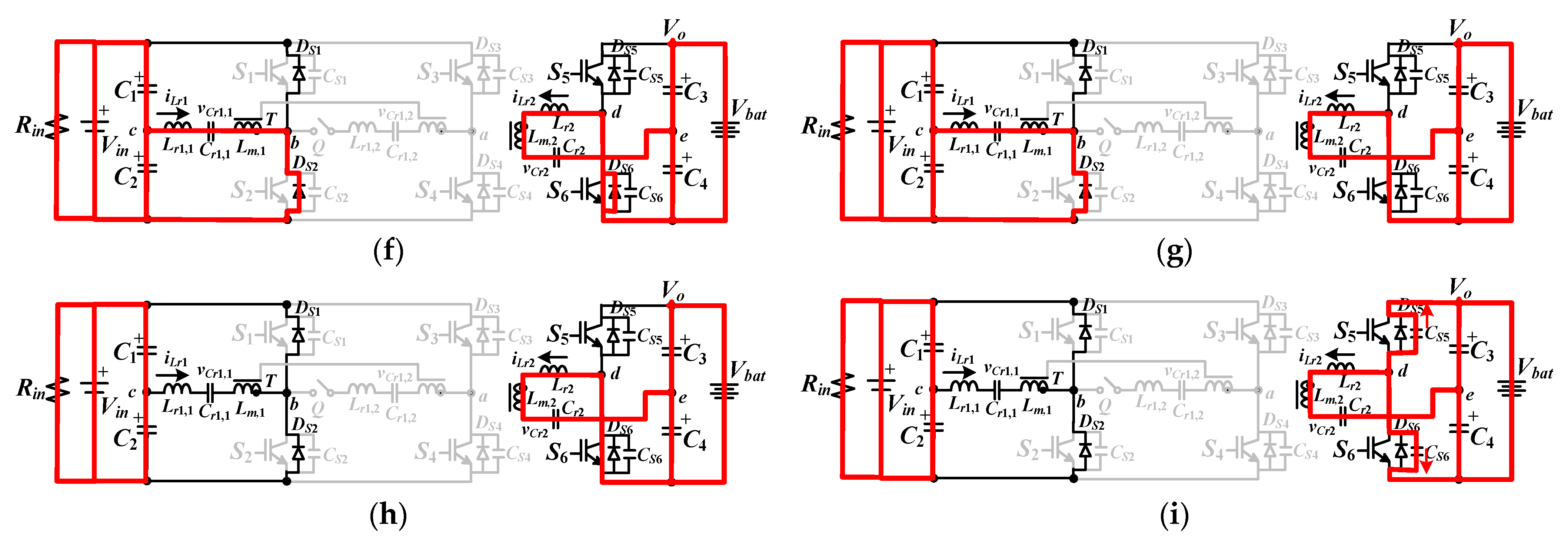
- State 5
- [t4 ≤ t < t5]: vCS4 = 0 at t4 and DS4 becomes forward biased due to iLr1(t4) > 0. At this moment, S4 turns on under zero voltage. In state 5, iLr2 < 0 and DS6 is conducting to charge C4.
- State 6
- [t5 ≤ t < t6]: Since Vac = −VC2 = −Vin/2, iLr1 is decreased and becomes negative at time t5. Then, the primary current iLr1 will flow through S4 instead of DS4. Forward power flow is from C2 to charge C4.
- State 7
- [t6 ≤ t < t7]: iLr2 = 0 at t = t6 and DS6 turns off. The primary side current iLr1 flows through C2, Lr1,1, Cr1,1, Lm,1, Lr1,2, Cr1,2, and S4.
- State 8
- [t7 ≤ t < Tsw+t0]: S4 turns off at t = t7. Then, CS3 is discharged and CS4 is charged by current iLr1. This state is terminated at Tsw + t0.
2.2. Forward Power Conversion and High Voltage Output
2.3. Reverse Power Conversion
- State 1
- [t0 ≤ t < t1]: The capacitor voltage vCS5 is decreased to zero at t5. Then, DS5 becomes forward biased due to iLr2(t0) being negative. At this moment, the zero voltage turn-on of S5 can be achieved. Since iLr1 is positive, DS1 is conducting to charge C1.
- State 2
- [t1 ≤ t < t2]: Since Vde > 0 in this state, iLr2 is increased and has a positive value after time t1. Therefore, iLr2 flows through S5 instead of DS5. Reverse power flow is from VC3 to VC1.
- State 3
- [t2 ≤ t < t3]: iLr1 = 0 at time t2 and DS1 turns off. Then, iLr2 is equal to the magnetizing current iLm2.
- State 4
- [t3 ≤ t < t4]: S5 turns off at t = t3 and iLr2(t3) > 0. Thus, CS5 (CS6) is charged (discharged).
- State 5
- [t4 ≤ t < t5]: The capacitor voltage vCS6 is decreased to zero at t = t4. Then, DS6 becomes forward biased due to iLr2(t4) being positive. After time t4, the zero voltage turn-on of S6 can be realized. In state 5, iLr1(t) is negative and DS2 becomes forward biased. Since the leg voltage Vde = −VC4, iLr2 decreases in this state.
- State 6
- [t5 ≤ t < t6]: After time t5, iLr2 < 0. Then, iLr,2 flows through switch S6 instead of diode DS6. Reverse power conversion is achieved from the VC4 terminal to VC2 terminal.
- State 7
- [t6 ≤ t < t7]: The left-hand side current iLr1 = 0 at time t6 and DS2 becomes reverse biased.
- State 8
- [t7 ≤ t < Tsw+t0]: S6 turns off at time t7 and iLr,2 charges (discharges) CS6 (CS5). At time Tsw + t0, the switching cycle is completed.
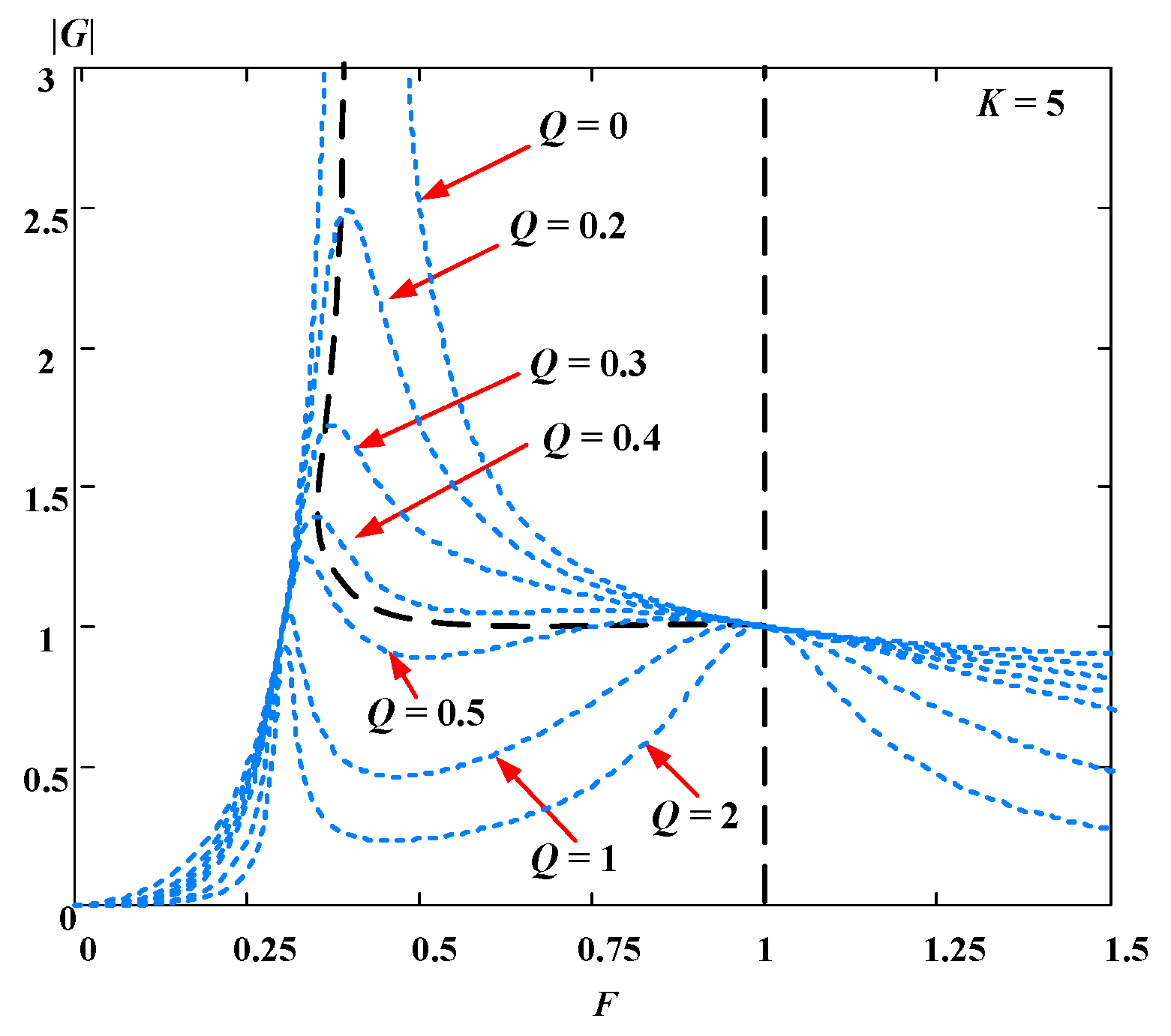
3. Circuit Properties and Design Example
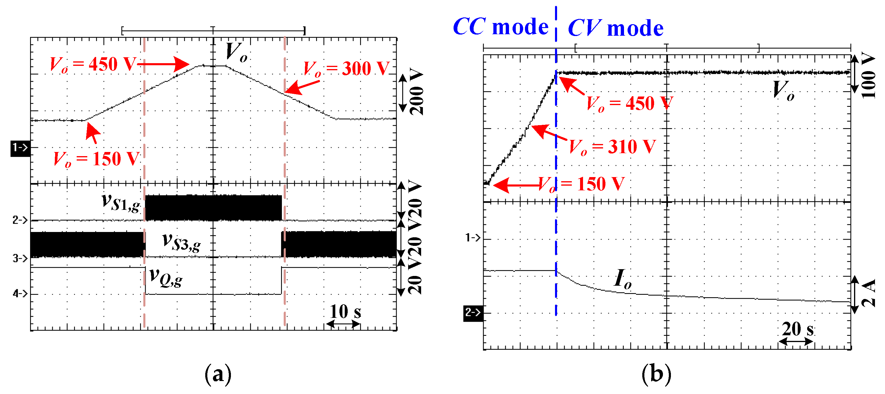
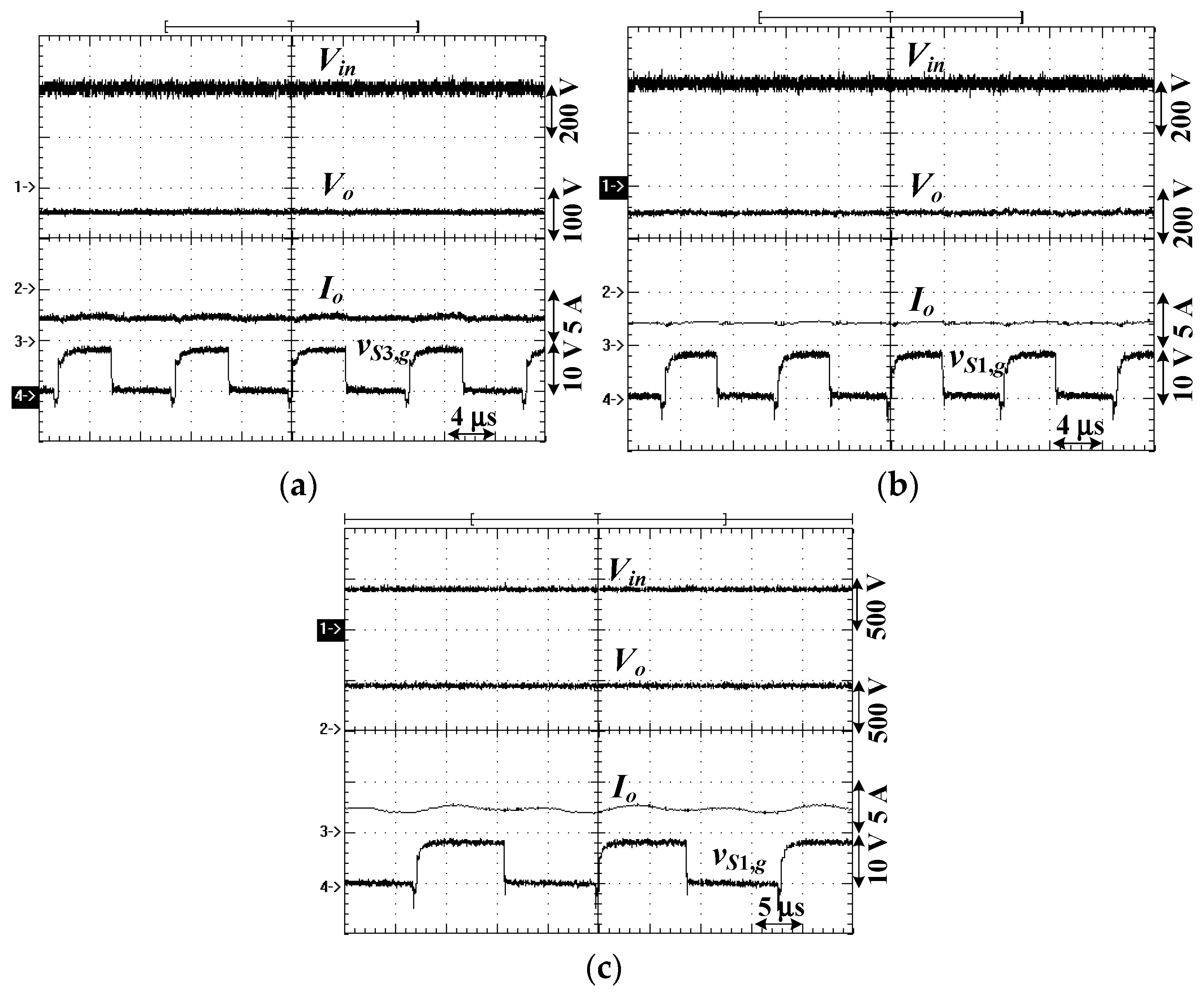
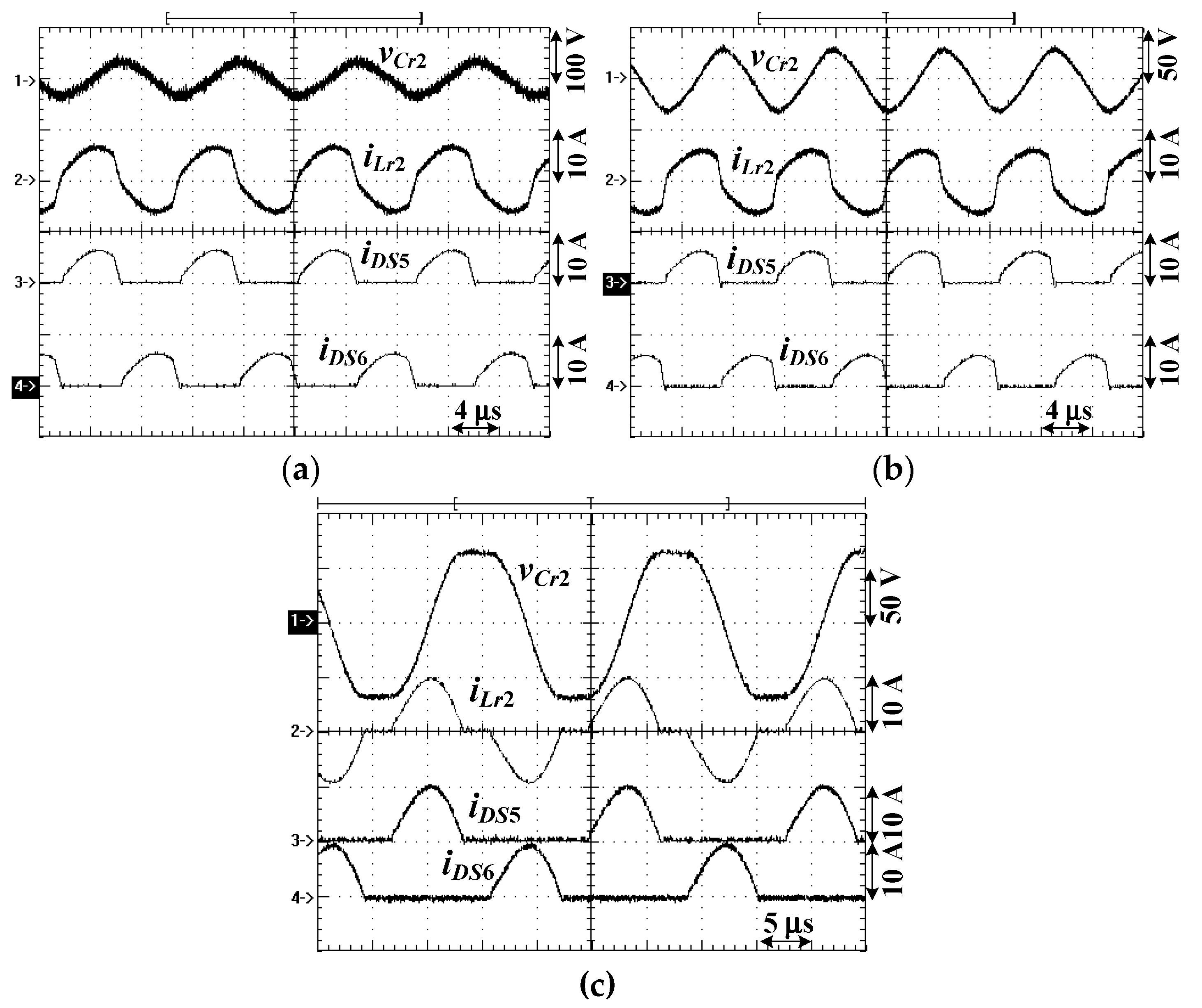
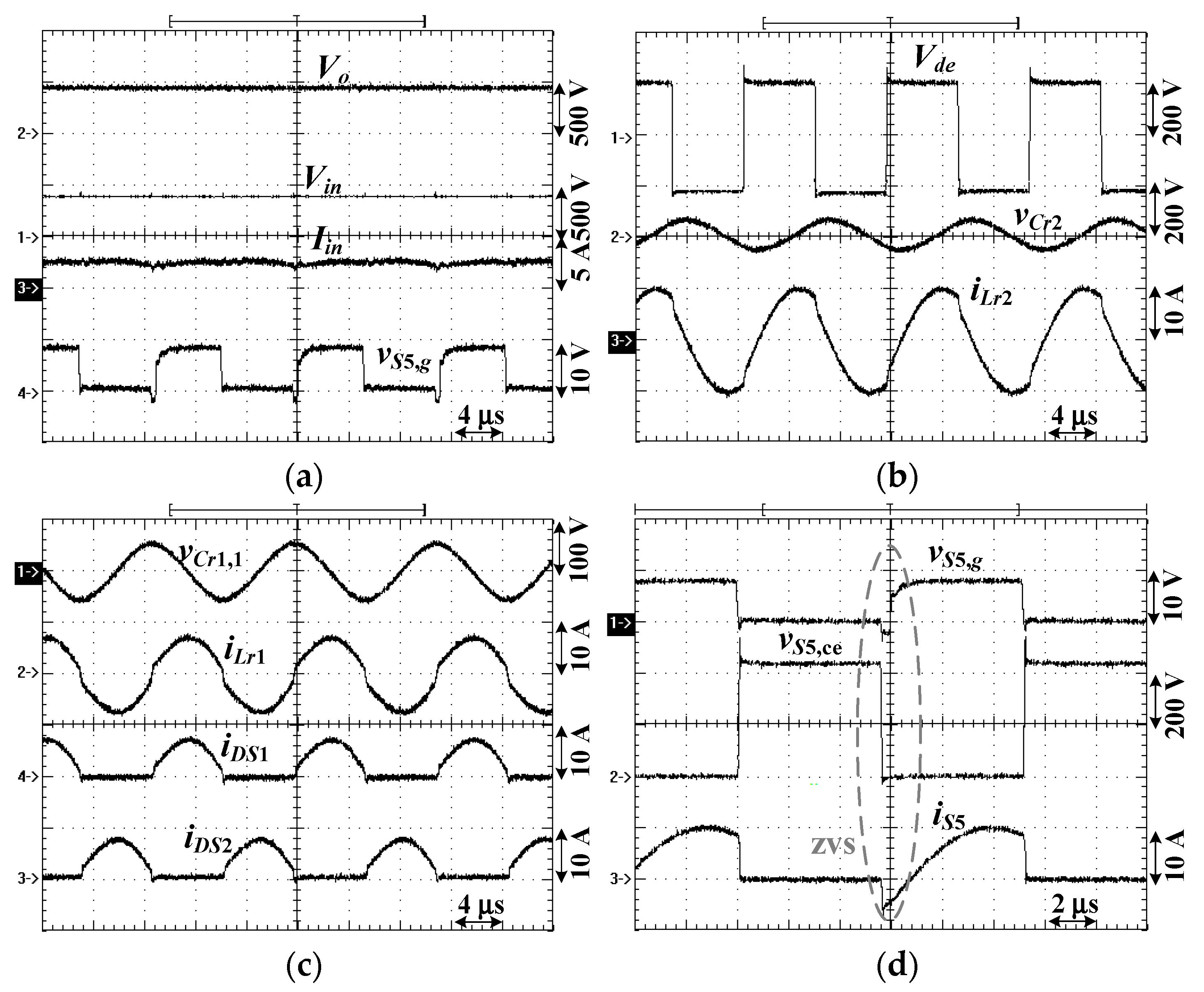
4. Experimental Verifications
5. Conclusions
Funding
Acknowledgments
Conflicts of Interest
References
- Mao, H.; Lee, C.Y.; Boroyevich, D.; Hiti, S. Review of high-performance three-phase power-factor correction circuits. IEEE Trans. Ind. Electron. 1997, 44, 437–446. [Google Scholar]
- Singh, B.; Singh, B.N.; Chandra, A.; Al-Haddad, K.; Pandey, A.; Kothari, D.P. A review of three-phase improved power quality AC-DC converters. IEEE Trans. Ind. Electron. 2004, 51, 641–660. [Google Scholar] [CrossRef]
- Guerrero, J.M.; Loh, P.C.; Lee, T.L.; Chandorkar, M. Advanced control architectures for intelligent microgrids—part II: Power quality, energy storage, and ac/dc microgrids. IEEE Trans. Ind. Electron. 2013, 60, 1263–1270. [Google Scholar] [CrossRef] [Green Version]
- Meng, L.; Shafiee, Q.; Trecate, G.F.; Karimi, H.; Fulwani, D.; Lu, X.; Guerrero, J.M. Review on control of DC microgrids and multiple microgrid clusters. IEEE J. Emerg. Sel. Top. Power Electron. 2017, 5, 928–948. [Google Scholar]
- Emadi, A.; Lee, Y.J.; Rajashekara, K. Power electronics and motor drives in electric, hybrid electric, and plug-in hybrid electric vehicles. IEEE Trans. Ind. Electron. 2008, 55, 2237–2245. [Google Scholar] [CrossRef]
- Ahrabi, R.R.; Ardi, H.; Elmi, M.; Ajami, A. A novel step-up multi input dc-dc converter for hybrid electric vehicles application. IEEE Trans. Power Electron. 2017, 32, 3549–3561. [Google Scholar] [CrossRef]
- Blaabjerg, F.; Dragicevic, T.; Davari, P. Applications of Power Electronics. Electronics 2019, 8, 465. [Google Scholar] [CrossRef] [Green Version]
- Mangu, B.; Akshatha, S.; Suryanarayana, D.; Fernandes, B.G. Grid-connected PV-wind-battery-based multi-input transformer-couple bidirectional dc-dc converter for household applications. IEEE J. Emerg. Sel. Top. Power Electron. 2016, 4, 1086–1095. [Google Scholar] [CrossRef]
- Xu, D.; Zhao, C.; Fan, H. A PWM plus phase-shift control bidirectional DC-DC converter. IEEE Trans. Ind. Electron. 2004, 19, 666–675. [Google Scholar] [CrossRef]
- Zhao, B.; Song, Q.; Liu, W.; Sun, Y. Overview of dual-active-bridge isolated bidirectional DC–DC converter for high-frequency-link power-conversion system. IEEE Trans. Power Electron. 2014, 29, 4091–4106. [Google Scholar] [CrossRef]
- Rico, S.J.; Pagano, D.J.; Lucas, K.E. Bidirectional power sharing for DC microgrid enabled by dual active bridge DC-DC converter. Energies 2021, 14, 404. [Google Scholar] [CrossRef]
- Jung, J.H.; Kim, H.S.; Ryu, M.H.; Baek, J.W. Design methodology of bidirectional CLLC resonant converter for high-frequency isolation of DC distribution systems. IEEE Trans. Power Electron. 2013, 28, 1741–1755. [Google Scholar] [CrossRef]
- Liu, Y.; Du, G.; Wang, X.; Lei, Y. Analysis and Design of High-Efficiency Bidirectional GaN-Based CLLC Resonant Converter. Energies 2019, 12, 2859. [Google Scholar] [CrossRef] [Green Version]
- Zou, S.; Lu, J.; Mallik, A.; Khaligh, A. Bi-directional CLLC converter with synchronous rectification for plug-in electric vehicles. IEEE Trans. Ind. Appl. 2018, 54, 998–1005. [Google Scholar] [CrossRef]
- Lin, B.R. Analysis of a series-parallel resonant converter for DC microgrid applications. Processes 2021, 9, 542. [Google Scholar] [CrossRef]
- Lin, B.R. Analysis and implementation of a frequency control DC-DC converter for light electric vehicle applications. Electronics 2021, 10, 1623. [Google Scholar] [CrossRef]
- Lin, B.B.; Chen, K.Y. Hybrid LLC Converter with Wide Range of Zero-Voltage Switching and Wide Input Voltage Operation. Appl. Sci. 2020, 10, 8250. [Google Scholar] [CrossRef]
- Wang, P.; Zhou, L.; Zhang, Y.; Li, J.; Sumner, M. Input-parallel output-series DC-DC boost converter with a wide input voltage range, for fuel cell vehicles. IEEE Trans. Veh. Technol. 2017, 66, 7771–7781. [Google Scholar] [CrossRef]
- Hu, H.; Fang, X.; Chen, F.; Shen, Z.J.; Batarseh, I. A modified high-efficiency LLC converter with two transformers for wide input-voltage range applications. IEEE Trans. Power Electron. 2013, 28, 1946–1960. [Google Scholar] [CrossRef]
- Steigerwald, R.L. A Comparison of Half-Bridge Resonant Converter Topologies. IEEE Trans. Power Electron. 1988, 3, 174–182. [Google Scholar] [CrossRef]


| Primary-Side | Secondary-Side | Input/Output Voltages | Power Flow Direction | Control Scheme | |
|---|---|---|---|---|---|
| Proposed circuit | Half-bridge circuit | Half-bridge circuit | Vin = 400 V Vo = 150–450 V | Voltage step-up/step-down for bidirectional power flow | Frequency control |
| Circuit structure in [9] | Half-bridge circuit | Half-bridge circuit | Vin = 48 V Vo = 24–30 V | Voltage step-down for forward power flow and voltage step-up for reverse power flow | Phase shift + PWM control |
| Circuit structure in [11] | Full-bridge circuit | Full-bridge circuit | Vin = 400 V Vo =400 V | Voltage step-up/step-down for bidirectional power flow | Phase shift + PWM control |
| Circuit structure in [13] | Full-bridge circuit | Full-bridge circuit | Vin = 382–408 V Vo = 400 V | Voltage step-up/step-down for bidirectional power flow | Frequency control |
| Circuit structure in [15] | Cascade half-bridge circuit | Parallel center-tapped rectifier | Vin = 750–800 V Vo = 24 V | Voltage step-up/step-down for forward power flow | Frequency control |
| Items | Parameter |
|---|---|
| C1, C2 | 660 μF |
| C3, C4 | 660 μF |
| Cr1,1, Cr1,2 | 144 nF |
| Cr2 | 243 nF |
| Lr1,1, Lr1,2 | 27.45 μH |
| Lr2 | 16.24 μH |
| Lm,1 | 137.25 μH |
| S1–S6 | GP50B60PD1 (600 V/33 A) |
| Q | 6R125P6 (650 V/19 A) |
| Transformer np1:np2:ns | 26:26:20 |
Publisher’s Note: MDPI stays neutral with regard to jurisdictional claims in published maps and institutional affiliations. |
© 2022 by the author. Licensee MDPI, Basel, Switzerland. This article is an open access article distributed under the terms and conditions of the Creative Commons Attribution (CC BY) license (https://creativecommons.org/licenses/by/4.0/).
Share and Cite
Lin, B.-R. Analysis and Implementation of a Bidirectional Converter with Soft Switching Operation. Processes 2022, 10, 561. https://doi.org/10.3390/pr10030561
Lin B-R. Analysis and Implementation of a Bidirectional Converter with Soft Switching Operation. Processes. 2022; 10(3):561. https://doi.org/10.3390/pr10030561
Chicago/Turabian StyleLin, Bor-Ren. 2022. "Analysis and Implementation of a Bidirectional Converter with Soft Switching Operation" Processes 10, no. 3: 561. https://doi.org/10.3390/pr10030561
APA StyleLin, B.-R. (2022). Analysis and Implementation of a Bidirectional Converter with Soft Switching Operation. Processes, 10(3), 561. https://doi.org/10.3390/pr10030561