
Design of a High Efficiency High Step-Up/Step-Down Bidirectional Isolated DC–DC Converter


Abstract
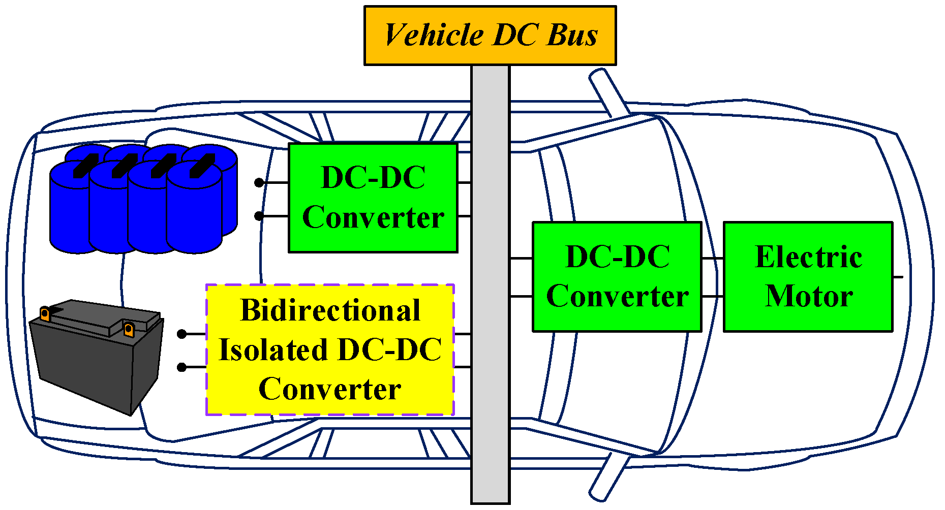
:1. Introduction
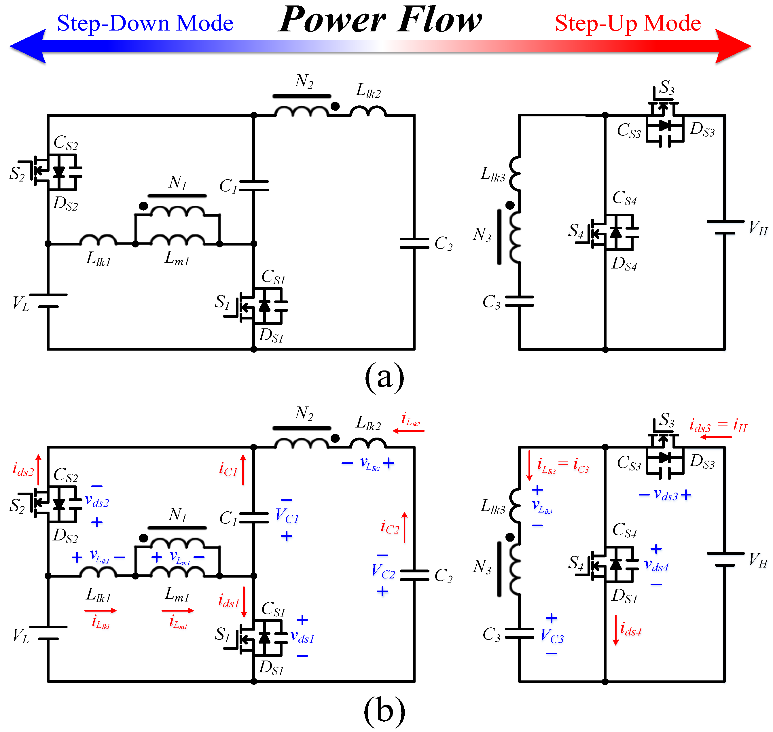
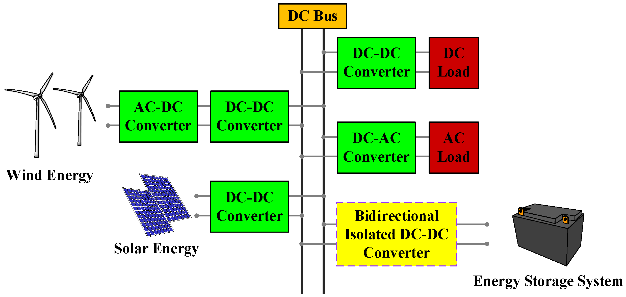
2. Circuit Architecture and Operational Principles
- (1)
- Switches and their parasitic diodes are ideal and the parasitic capacitance is considered.
- (2)
- The capacitance values C1, C2, and C3 are infinite.
- (3)
- The leakage inductance values Llk1 and Llk2 are substantially much lower than the magnetizing inductance Lm1.
- (4)
- N1 is equal to N2 but less than N3, and the ratios of N1/N3 and N2/N3 are defined as N.
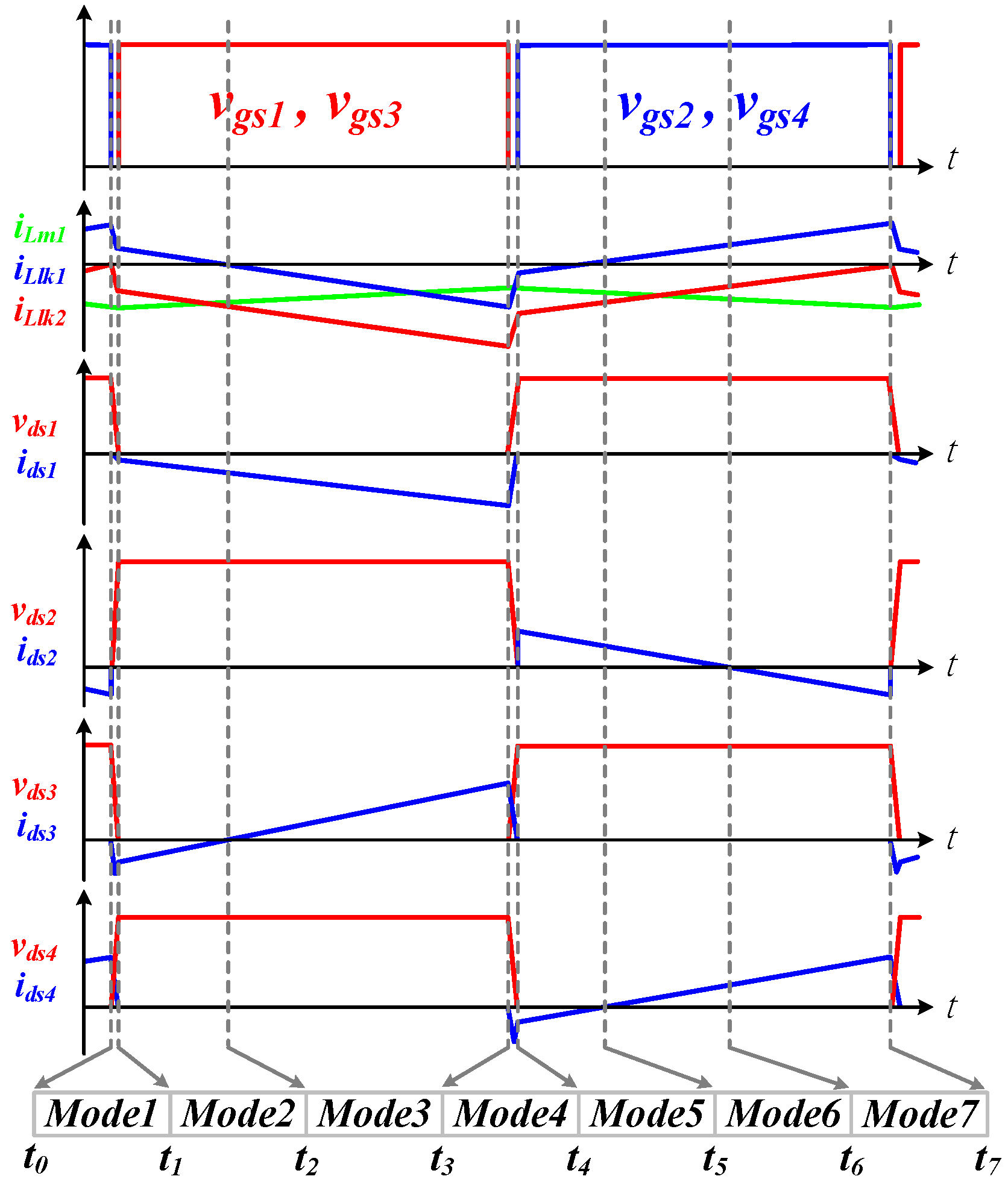
3. Steady-State Analysis
- (1)
- All components are ideal. The internal resistance and parasitic effects are ignored.
- (2)
- The capacitance of all capacitors is infinite, making the capacitor voltage constant.
- (3)
- The leakage inductance of the transformer is ignored.
- (4)
- The circuit operating modes with short durations are ignored.
- (5)
- For easier calculation, the ideal transformer is represented as N = N1/N3 = N2/N3, where N is the transformer turns ratio.
3.1. Step-Up Mode
3.1.1. Voltage Gain Analysis
3.1.2. Voltage Stress Analysis of Components
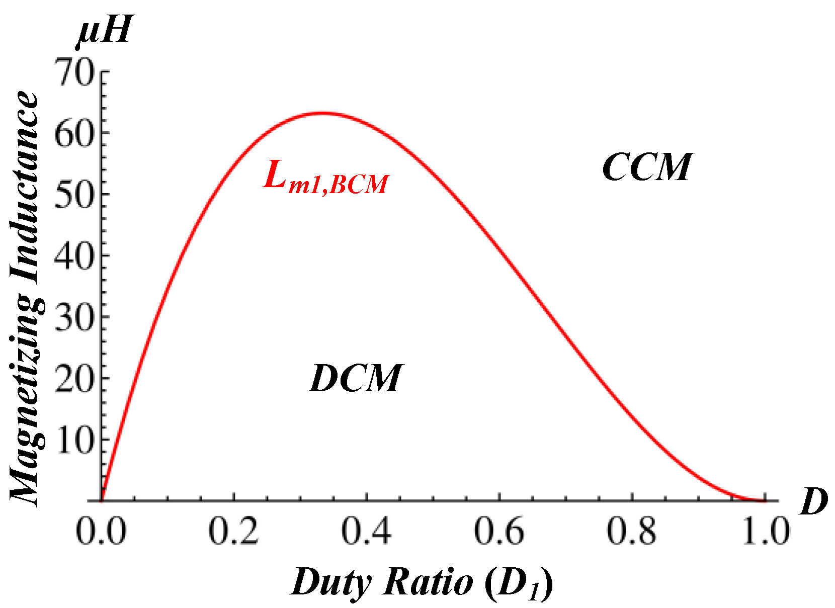
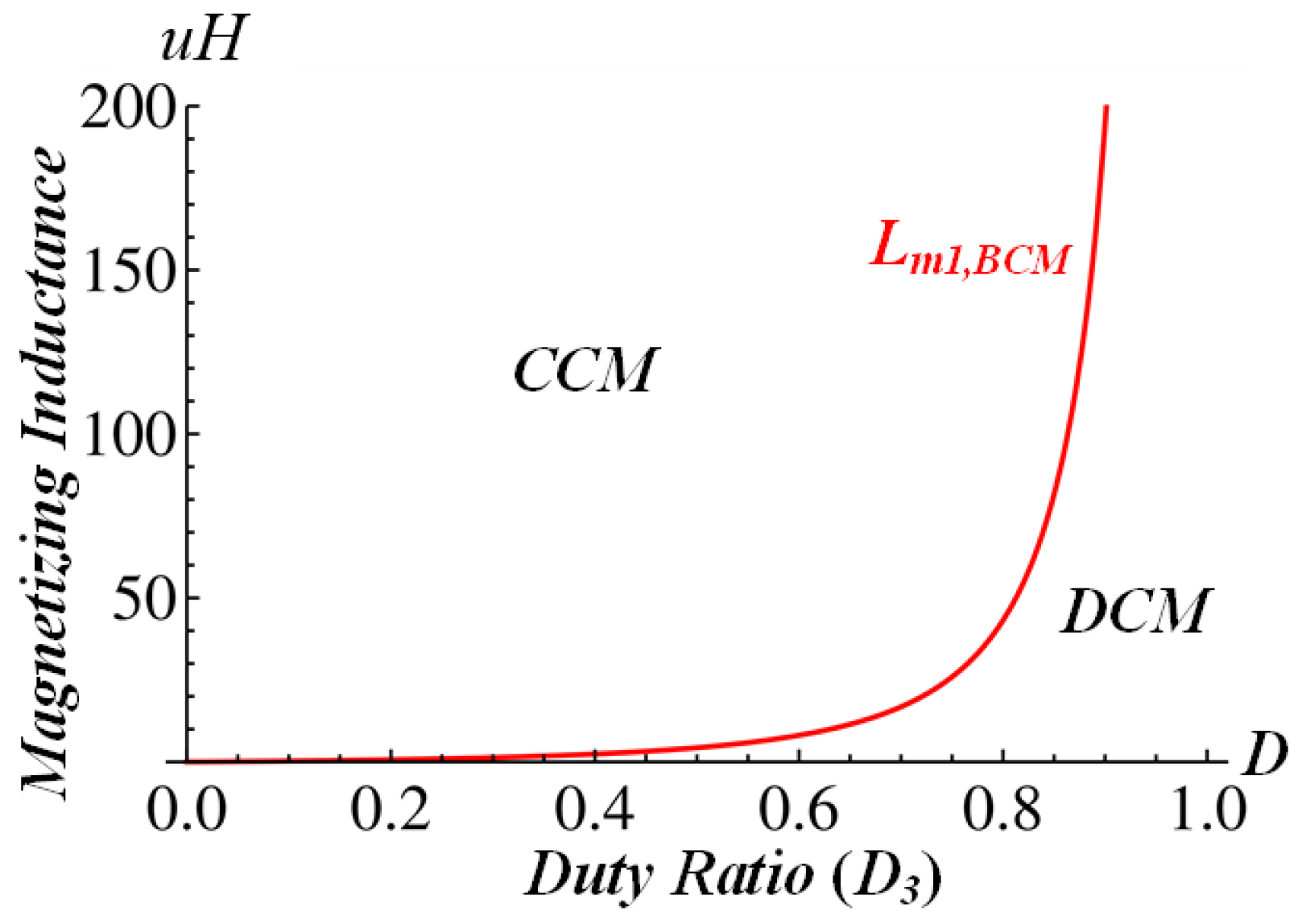
3.1.3. Design of the Magnetic Components
3.2. Step-Down Mode
3.2.1. Voltage Gain Analysis
3.2.2. Voltage Stress Analysis of Components
3.2.3. Design of the Magnetic Components
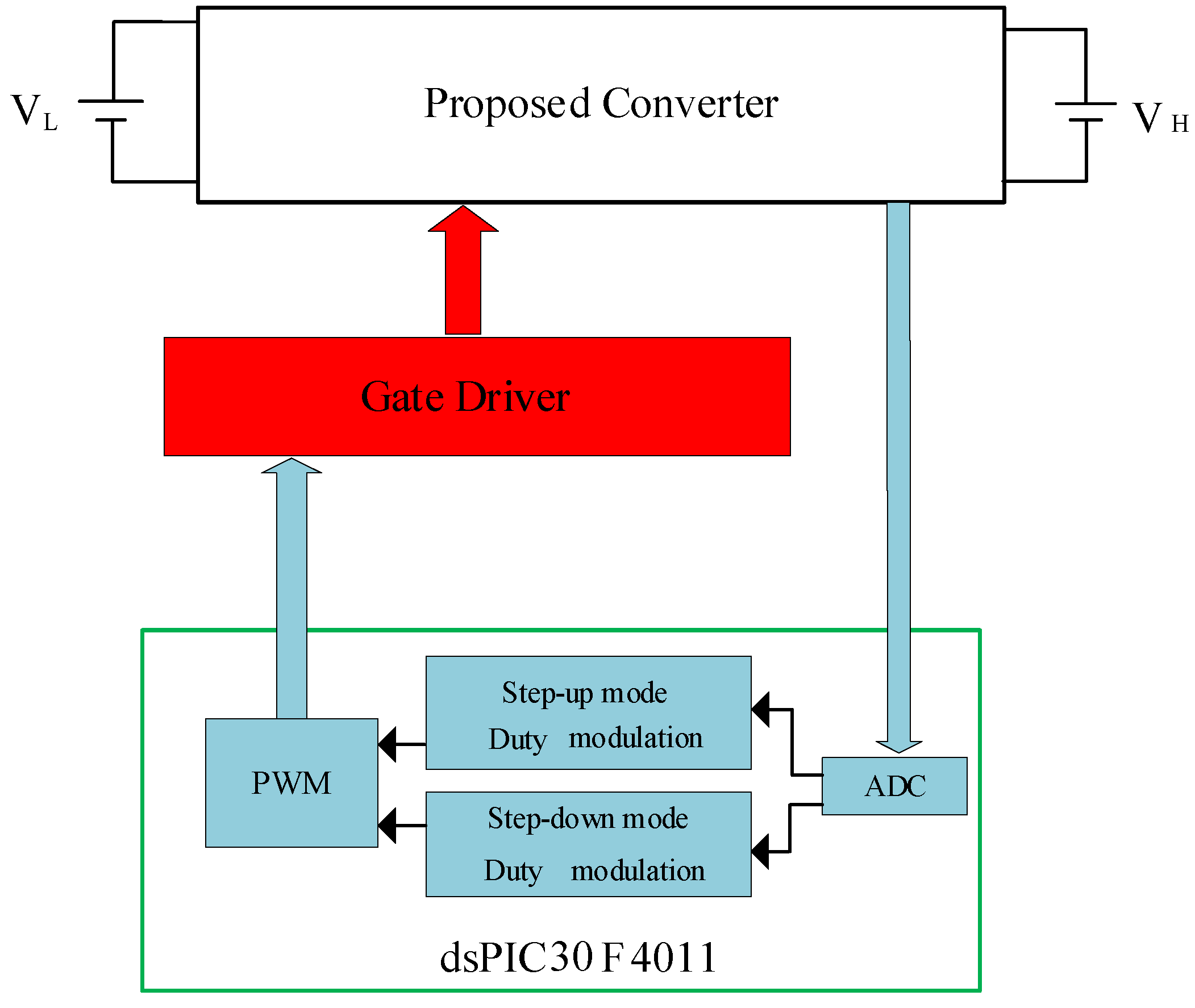
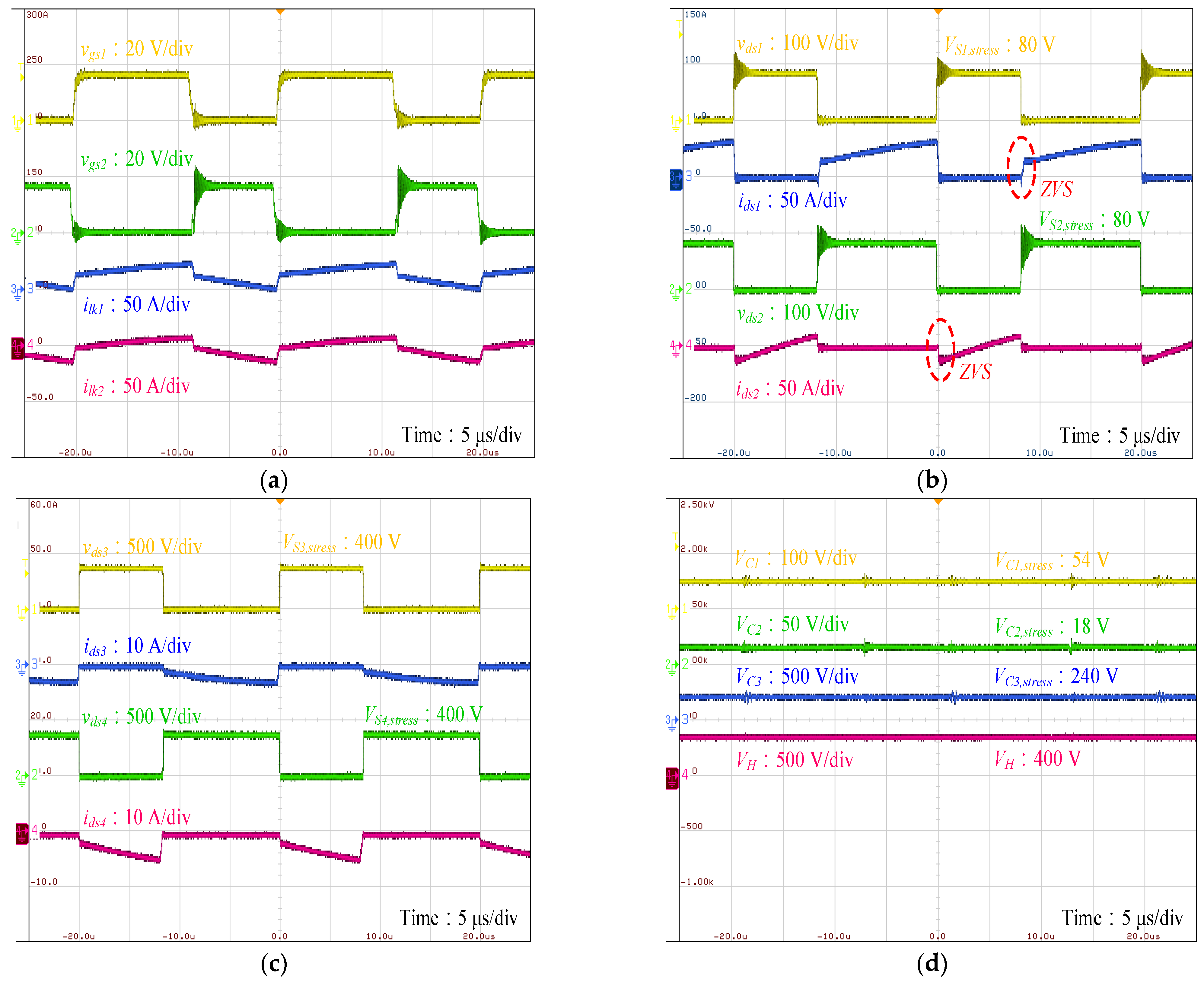
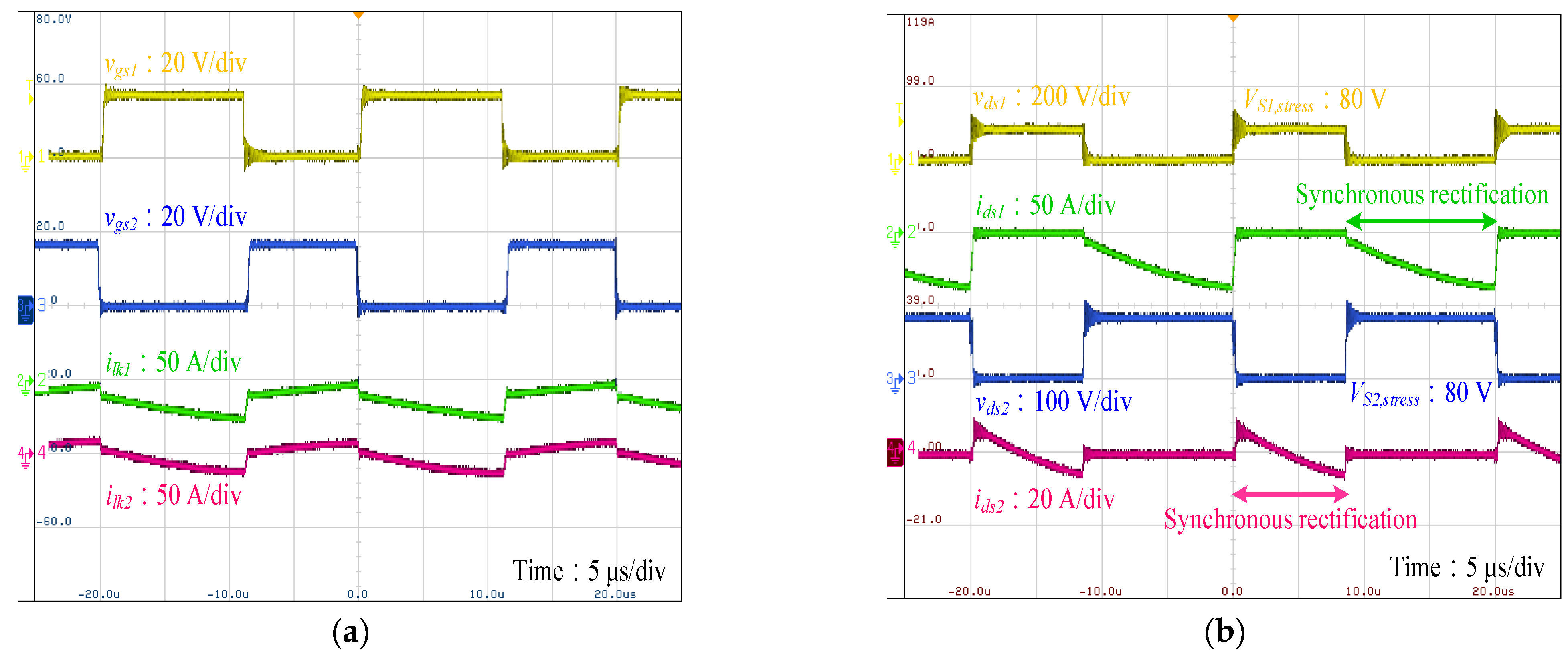
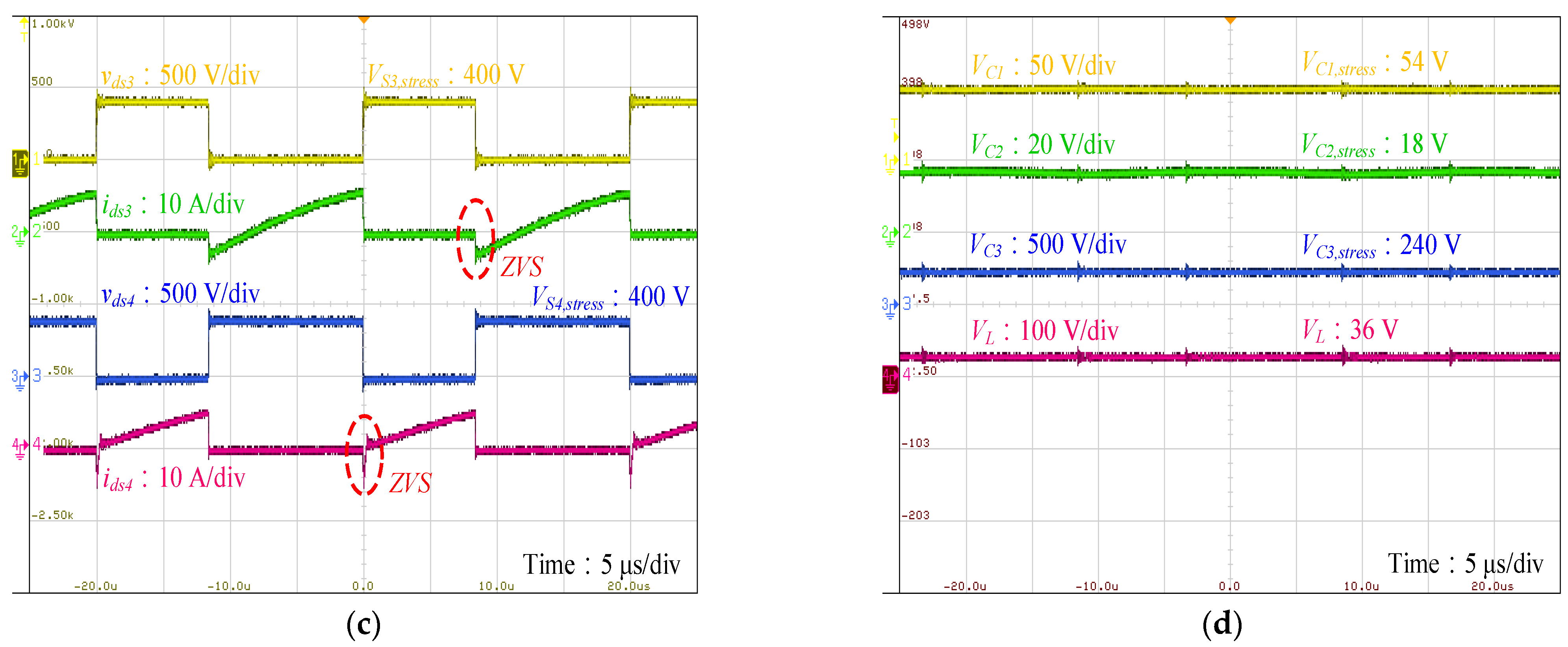
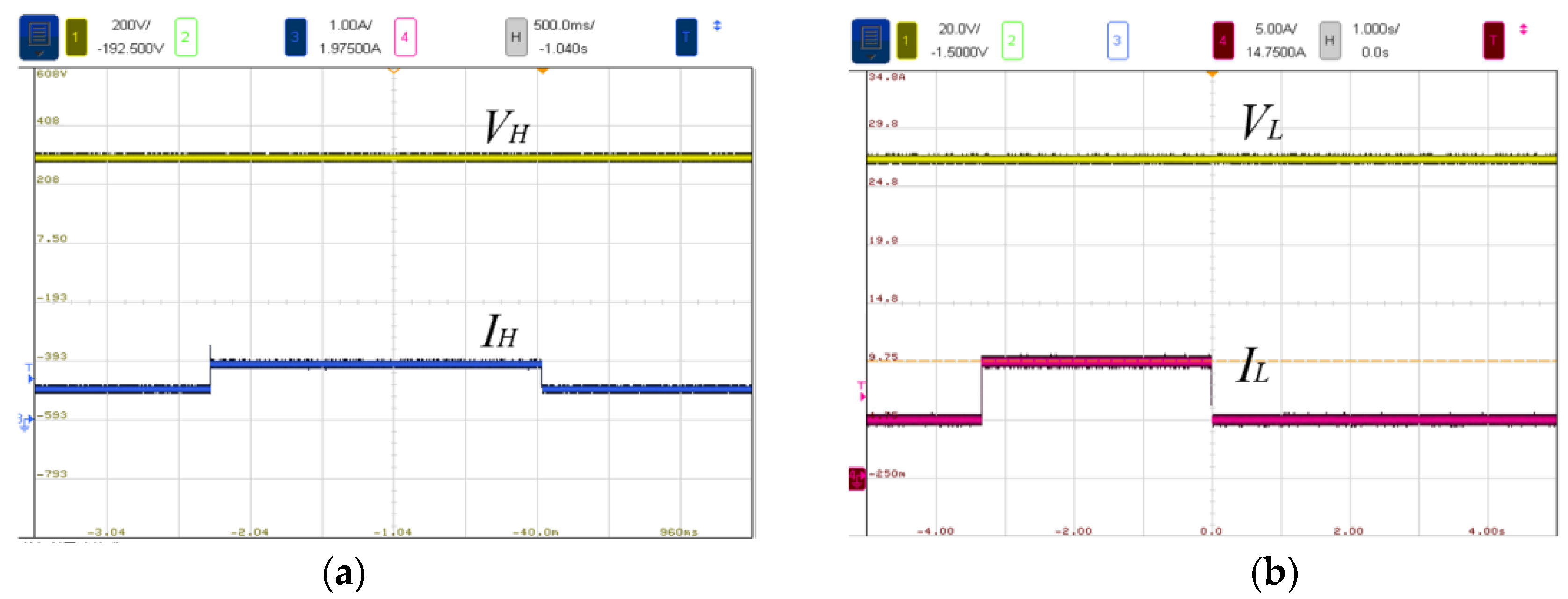
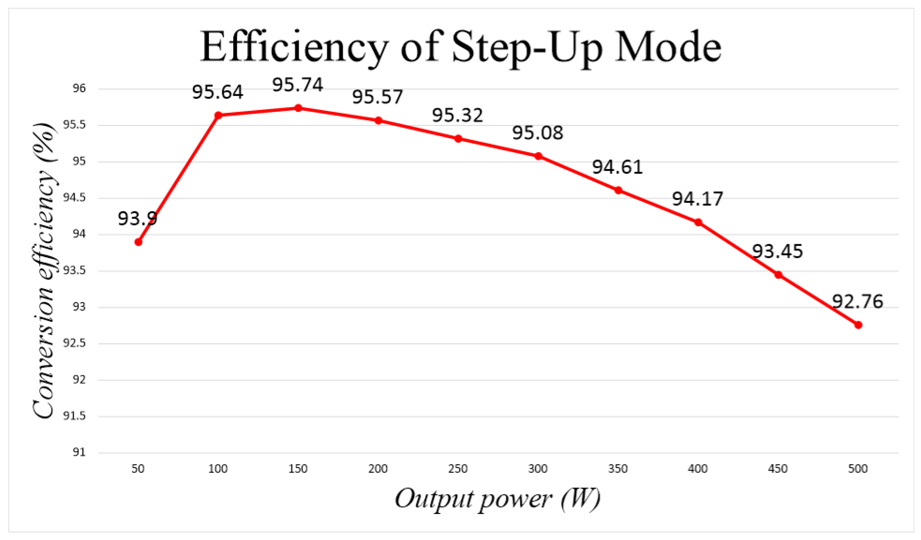
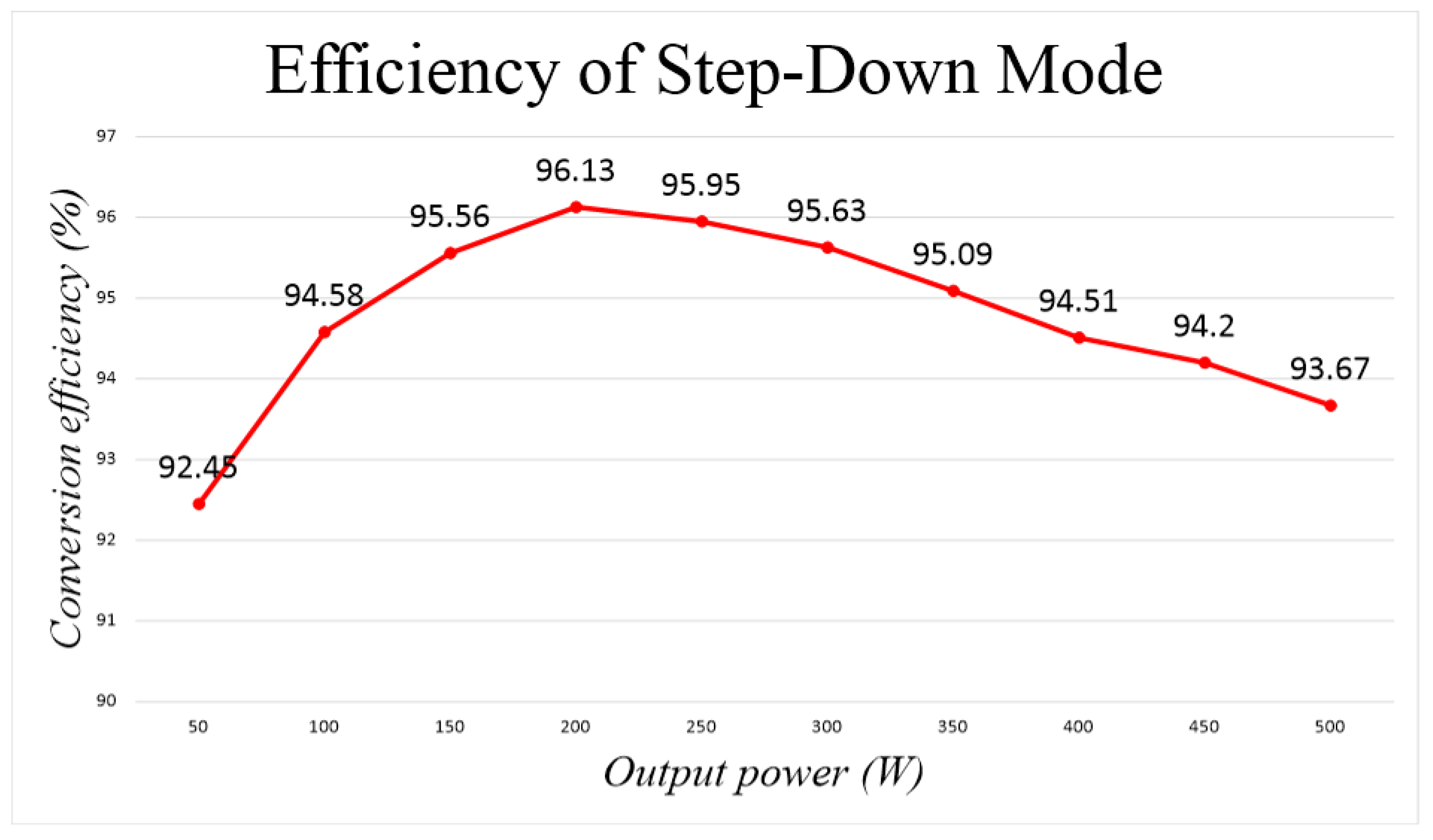
4. Experimental Results
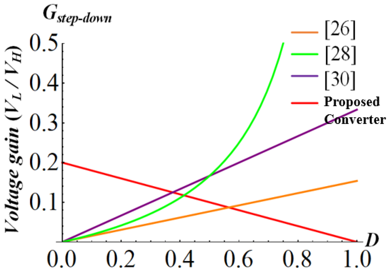
5. Discussion and Conclusions
Author Contributions
Funding
Institutional Review Board Statement
Informed Consent Statement
Data Availability Statement
Conflicts of Interest
References
- Drees, T.; Bracht, N.V.; Moser, A. Reserve providing in future generation systems considering renewable energy sources. In Proceedings of the 11th International Conference on the European Energy Market (EEM14), Krakow, Poland, 28–30 May 2014; Volume 14, pp. 1–6. [Google Scholar]
- Ahmed, A.; Jiang, T. Operation Management of Power Grid System with Renewable Energy Sources and Energy Storage System Integrations. In Proceedings of the 2nd IEEE Conference on Energy Internet and Energy System Integration, Beijing, China, 20–22 October 2018; pp. 1–6. [Google Scholar]
- Dahale, S.; Das, A.; Pindoriya, N.M.; Rajendran, S. An overview of DC-DC converter topologies and controls in DC microgrid. In Proceedings of the 7th International Conference on Power Systems (ICPS), Pune, India, 21–23 December 2017; pp. 410–415. [Google Scholar]
- Lonkar, M.; Ponnaluri, S. An overview of DC microgrid operation and control. In Proceedings of the IREC2015 the Sixth International Renewable Energy Congress, Sousse, Tunisia, 24–26 March 2015; pp. 1–6. [Google Scholar] [CrossRef]
- Joshi, R.P.; Deshmukh, A.P. Hybrid Electric Vehicles: The Next Generation Automobile Revolution. In Proceedings of the IEEE Conference on Electric and Hybrid Vehicles, Pune, India, 18–20 December 2006; pp. 1–6. [Google Scholar]
- Song, E.; Yao, C.; Fan, L. Analysis and investigation on PHEV Economy flow. In Proceedings of the 2011 International Conference on Electronics, Communications and Control (ICECC), Ningbo, China, 9–11 September 2011; pp. 4172–4175. [Google Scholar]
- Klassen, S.V.; Klassen, T.S.; Shtein, D.; Volkov, A.G.; Dubkova, R.Y.; Luft, S. Study of a Dual-Loop Subordinate Control System for a DC-DC Converter with Galvanic Isolation. In Proceedings of the 19th International Conference of Young Specialists on Micro/Nanotechnologies and Electron Devices, Erlagol, Russia, 29 June–3 July 2018; pp. 6403–6410. [Google Scholar]
- Hsieh, Y.-C.; Chang, Y.-N.; Lee, K.-Y.; Chiu, Y.-C.; Wu, W.-T. Bidirectional softly switched dc-to-dc converter with galvanic isolation. In Proceedings of the 2015 IEEE International Conference on Industrial Technology (ICIT), Seville, Spain, 17–19 March 2015; pp. 952–956. [Google Scholar]
- Arnaudov, D.; Hinov, N.; Vuchev, S.; Nedyalkov, I. Converter with galvanic isolation for supercapacitor charging. In Proceedings of the 19th International Symposium on Electrical Apparatus and Technologies (SIELA), Bourgas, Bulgaria, 29 May–1 June 2016; pp. 1–4. [Google Scholar]
- Hu, J.; Xiao, W.; Zhang, B.; Qiu, D.; Ho, C.N.M. A Single Phase Hybrid Interleaved Parallel Boost PFC Converter. In Proceedings of the Energy Conversion Congress and Exposition (ECCE), Portland, OR, USA, 23–27 September 2018; pp. 2855–2859. [Google Scholar]
- Ancuti, M.-C.; Svoboda, M.; Musuroi, S.; Hedes, A.; Olarescu, N.-V. Boost PFC converter versus bridgeless boost PFC converter EMI analysis. In Proceedings of the 2014 International Conference on Applied and Theoretical Electricity (ICATE), Craiova, Romania, 23–25 October 2014; pp. 1–6. [Google Scholar]
- Ye, Z.; Sun, B. PFC efficency improvement and THD reduction at light loads with ZVS and valley switching. In Proceedings of the Twenty-Seventh Annual IEEE Applied Power Electronics Conference and Exposition (APEC), Coronado Springs, OR, USA, 5–9 February 2012; pp. 802–806. [Google Scholar]
- Harrag, A.; Messalti, S.; Daili, Y. Innovative Single Sensor Neural Network PV MPPT. In Proceedings of the 2019 6th International Conference on Control, Decision and Information Technologies (CoDIT), Paris, France, 26–29 April 2019; pp. 1895–1899. [Google Scholar]
- Messalti, S.; Harrag, A.G.; Loukriz, A.E. A new neural networks MPPT controller for PV systems. In Proceedings of the IREC2015 The Sixth International Renewable Energy Congress, Sousse, Tunisia, 24–26 March 2015; pp. 1–6. [Google Scholar]
- Singh, A.; Shimi, S.L. MATLAB / SIMULINK Simulation of PV System Based on MPPT in Variable Irradiance with EV Battery as Load. In Proceedings of the International Conference on Computational Intelligence and Computing Research (ICCIC), Timilnadu, India, 14–16 December 2017; pp. 1–4. [Google Scholar]
- Tintu, V.R.; George, M. Tapped inductor technology based DC-DC converter. In Proceedings of the 2011 International Conference on Signal Processing, Communication, Computing and Networking Technologies, Thuckalay, India, 21–22 July 2011; pp. 747–753. [Google Scholar]
- Yris, J.C.; Calleja, J.H.; González, L.H.; López, L.M.; Martínez, R.P. Analysis of tapped inductor converters in three operating modes for photovoltaic systems with grounded source. In Proceedings of the 12th IEEE International Power Electronics Congress, San Luis Potosi, Mexico, 22–25 August 2010; pp. 215–220. [Google Scholar]
- Vazquez, N.; Estrada, L.; Hernandez, C.; Rodriguez, E. The Tapped-Inductor Boost Converter. In Proceedings of the International Symposium on Industrial Electronics, Vigo, Spain, 4–7 June 2007; pp. 538–543. [Google Scholar]
- Mohammed, A.A.; Nafie, S.M. Flyback converter design for low power application. In Proceedings of the 2015 International Conference on Computing, Control, Networking, Electronics and Embedded Systems Engineering (ICCNEEE), Khartoum, Sudan, 7–9 September 2015; pp. 447–450. [Google Scholar]
- Hsieh, Y.; Chen, J.; Yang, L.; Wu, C.; Liu, W. High-Conversion-Ratio Bidirectional DC–DC Converter with Coupled In-ductor. IEEE Trans. Ind. Electron. 2014, 61, 210–222. [Google Scholar] [CrossRef]
- Aamir, M.; Mekhilef, S.; Kim, H.-J. High-Gain Zero-Voltage Switching Bidirectional Converter with a Reduced Number of Switches. IEEE Trans. Circuits Syst. II Express Briefs 2015, 62, 816–820. [Google Scholar] [CrossRef]
- Dung, N.A.; Chiu, H.-J.; Liu, Y.-C.; Huang, P.J. Analysis and Implementation of a High Voltage Gain 1 MHz Bidirectional DC–DC Converter. Trans. Ind. Electron. 2020, 67, 1415–1424. [Google Scholar] [CrossRef]
- Omara, A.M.; Sleptsov, M. Bidirectional interleaved DC/DC converter for electric vehicle application. In Proceedings of the 11th International Forum on Strategic Technology (IFOST), Novosibirsk, Russia, 1–3 June 2016; pp. 100–104. [Google Scholar]
- Bahrami, H.; Farhangi, S.; Iman-Eini, H.; Adib, E. A New Interleaved Coupled-Inductor Nonisolated Soft-Switching Bidirectional DC–DC Converter with High Voltage Gain Ratio. IEEE Trans. Ind. Electron. 2017, 65, 5529–5538. [Google Scholar] [CrossRef]
- Yang, Y.; Ma, J.; Ho, C.N.-M.; Zou, Y. A New Coupled-Inductor Structure for Interleaving Bidirectional DC-DC Converters. IEEE J. Emerg. Sel. Top. Power Electron. 2015, 3, 841–849. [Google Scholar] [CrossRef]
- Hassan, W.; Soon, J.L.; Lu, D.D.-C.; Xiao, W. A High Conversion Ratio and High-Efficiency Bidirectional DC–DC Converter with Reduced Voltage Stress. IEEE Trans. Power Electron. 2020, 35, 11827–11842. [Google Scholar] [CrossRef]
- Hosseinzadeh, Z.; Molavi, N.; Farzanehfard, H. Soft-Switching High Step-Up/Down Bidirectional DC–DC Converter. IEEE Trans. Ind. Electron. 2019, 66, 4379–4386. [Google Scholar] [CrossRef]
- Liang, T.-J.; Lee, J.-H. Novel High-Conversion-Ratio High-Efficiency Isolated Bidirectional DC–DC Converter. IEEE Trans. Ind. Electron. 2014, 62, 4492–4503. [Google Scholar] [CrossRef]
- Shen, C.; Shen, Y.; Chiu, P.; Liang, T. Isolated bidirectional converter with minimum active switches for high-voltage ratio achievement and micro-grid applications. IET Power Electron. 2017, 10, 2208–2216. [Google Scholar] [CrossRef]
- Shen, C.-L.; Liou, H.; Liang, T.-C.; Gong, H.-Z. An Isolated Bidirectional Interleaved Converter with Minimum Active Switches and High Conversion Ratio. IEEE Trans. Ind. Electron. 2017, 65, 2313–2321. [Google Scholar] [CrossRef]
- Mukhtar, N.M.; Lu, D.D.-C. A Bidirectional Two-Switch Flyback Converter with Cross-Coupled LCD Snubbers for Minimizing Circulating Current. IEEE Trans. Ind. Electron. 2019, 66, 5948–5957. [Google Scholar] [CrossRef]
- Dutta, S.; Maiti, D.; Sil, A.K.; Biswas, S.K. A Soft-Switched Flyback converter with recovery of stored energy in leakage inductance. In Proceedings of the 5th India International Conference on Power Electronics, Delhi, India, 6–8 December 2012; pp. 1–5. [Google Scholar]
- Cheng, H.-L.; Chang, Y.-N.; Yen, H.-C.; Hua, C.-C.; Su, P.-S. An Interleaved Flyback-Typed LED Driver with ZVS and Energy Recovery of Leakage Inductance. IEEE Trans. Power Electron. 2019, 34, 4497–4508. [Google Scholar] [CrossRef]
- Lodh, T.; Majumder, T. High gain and efficient integrated flyback-Sepic DC-DC converter with leakage energy recovery mechanism. In Proceedings of the International Conference on Signal Processing, Communication, Power and Embedded System (SCOPES), Paralakhemundi, India, 3–5 October 2016; pp. 1495–1500. [Google Scholar]
- Chen, B.; Wang, P.; Wang, Y.-F.; Zhang, S.-H.; Yang, L.; Ji, R.-L. A Bidirectional CDT-LC Resonant DC–DC Converter with a Wide Voltage Range. IEEE Trans. Ind. Electron. 2019, 67, 2009–2020. [Google Scholar] [CrossRef]
- Tseng, K.-C.; Chang, S.-Y.; Cheng, C.-A. Novel Isolated Bidirectional Interleaved Converter for Renewable Energy Applications. IEEE Trans. Ind. Electron. 2019, 66, 9278–9287. [Google Scholar] [CrossRef]
- Lu, J.; Wang, Y.; Li, X. Isolated Bidirectional DC–DC Converter with Quasi-Resonant Zero-Voltage Switching for Battery Charge Equalization. IEEE Trans. Power Electron. 2019, 34, 4388–4406. [Google Scholar] [CrossRef]
- Sha, D.; Chen, D.; Zhang, J. A Bidirectional Three-Level DC–DC Converter with Reduced Circulating Loss and Fully ZVS Achievement for Battery Charging/Discharging. IEEE J. Emerg. Sel. Top. Power Electron. 2018, 6, 993–1003. [Google Scholar] [CrossRef]
- Saadatizadeh, Z.; Babaei, E.; Blaabjerg, F.; Cecati, C. Three-Port High Step-Up and High Step-Down DC-DC Converter with Zero Input Current Ripple. IEEE Trans. Power Electron. 2020, 36, 1804–1813. [Google Scholar] [CrossRef]
- Cheraghi, R.; Adib, E.; Golsorkhi, M.S. A Nonisolated High Step-Up Three-Port Soft-Switched Converter with Minimum witches. IEEE Trans. Ind. Electron. 2021, 68, 9358–9365. [Google Scholar] [CrossRef]
- Faraji, R.; Farzanehfard, H.; Esteki, M.; Khajehoddin, S.A. A Lossless Passive Snubber Circuit for Three-Port DC-DC Converter. IEEE J. Emerg. Sel. Top. Power Electron. 2021, 9, 1905–1914. [Google Scholar] [CrossRef]


| Parameter | Specification | Parameter | Specification |
|---|---|---|---|
| High-side voltage VH | 400 V | Switching frequency fs | 50 kHz |
| Low-side voltage VL | 36 V | Magnetizing inductance Lm1 | 47 μH |
| High-side power PH | 500 W | Leakage inductance Llk1 | 4 μH |
| Low-side power PL | 500 W | Leakage inductance Llk2 | 4 μH |
| Power switches S1 and S2 | IRFP4568PbF | Capacitor C1 | 100 μF |
| Power switches S3 and S4 | IXFH26N50Q | Capacitor C2 | 100 μF |
| Turns ration N | 5 | Capacitor C3 | 100 μF |
| Converter in [26] | Converter in [28] | Converter in [30] | Proposed Converter | |
|---|---|---|---|---|
| MOSFETs | 4 | 4 | 4 | 4 |
| Inductors | 0 | 2 | 1 | 0 |
| Transformers | 1 | 1 | 2 | 1 |
| Capacitors | 2 | 1 | 4 | 3 |
| Diodes | 0 | 0 | 6 | 0 |
| Turns ratio | 1:4.5 | 1:1.5 | 1:3 | 1:5 |
| The current ripple of low voltage side | Normal | Normal | Large | Normal |
| Low side Voltage VL | 30 V | 24 V | 48 V | 36 V |
| High side Voltage VH | 380 V | 200 V | 400 V | 400 V |
| Switching frequency fS | 50 kHz | 50 kHz | 40 kHz | 50 kHz |
| Output power | 300 W | 200 W | 400 W | 500 W |
| Isolated | No | Yes | Yes | Yes |
Publisher’s Note: MDPI stays neutral with regard to jurisdictional claims in published maps and institutional affiliations. |
© 2021 by the authors. Licensee MDPI, Basel, Switzerland. This article is an open access article distributed under the terms and conditions of the Creative Commons Attribution (CC BY) license (https://creativecommons.org/licenses/by/4.0/).
Share and Cite
Wu, Y.-E.; Lin, P.-J. Design of a High Efficiency High Step-Up/Step-Down Bidirectional Isolated DC–DC Converter. Processes 2022, 10, 50. https://doi.org/10.3390/pr10010050
Wu Y-E, Lin P-J. Design of a High Efficiency High Step-Up/Step-Down Bidirectional Isolated DC–DC Converter. Processes. 2022; 10(1):50. https://doi.org/10.3390/pr10010050
Chicago/Turabian StyleWu, Yu-En, and Pin-Jyun Lin. 2022. "Design of a High Efficiency High Step-Up/Step-Down Bidirectional Isolated DC–DC Converter" Processes 10, no. 1: 50. https://doi.org/10.3390/pr10010050
APA StyleWu, Y.-E., & Lin, P.-J. (2022). Design of a High Efficiency High Step-Up/Step-Down Bidirectional Isolated DC–DC Converter. Processes, 10(1), 50. https://doi.org/10.3390/pr10010050