Article

Fabrication of Gas-Sensor Chips Based on Silicon–Carbon Films Obtained by Electrochemical Deposition

by
Tatiana N. Myasoedova
1,*,
Mikhail N. Grigoryev
2,
Nina K. Plugotarenko
1 and
Tatiana S. Mikhailova
1
1
Institute of Nanotechnologies, Electronics and Equipment Engineering, Southern Federal University, Chekhov str. 2, 347928 Taganrog, Russia
2
Department for the production of microelectronic products, JSC “Taganrog Scientific-Research Institute of Communication”, 347913 Taganrog, Russia
*
Author to whom correspondence should be addressed.
Chemosensors 2019, 7(4), 52; https://doi.org/10.3390/chemosensors7040052
Submission received: 25 September 2019 / Revised: 21 October 2019 / Accepted: 28 October 2019 / Published: 30 October 2019
(This article belongs to the Special Issue Chemical Sensors for Air Quality Monitoring)

Abstract

:
In this study, we designed two types of gas-sensor chips with silicon–carbon film, doped with CuO, as the sensitive layer. The first type of gas-sensor chip consists of an Al2O3 substrate with a conductive chromium sublayer of ~10 nm thickness and 200 Ω/□ surface resistance, deposited by magnetron sputtering. The second type was fabricated via the electrochemical deposition of a silicon–carbon film onto a dielectric substrate with copper electrodes formed by photoelectrochemical etching. The gas sensors are sensitive to the presence of CO and CH4 impurities in the air at operating temperatures above 150 °C, and demonstrated p- (type-1) and n-type (type-2) conductivity. The type-1 gas sensor showed fast response and recovery time but low sensitivity, while the type-2 sensor was characterized by high sensitivity but longer response and recovery time. The silicon–carbon films were characterized by the presence of the hexagonal 6H SiC polytype with the impurities of the rhombohedral 15 R SiC phase. XRD analysis revealed the presence of a CuO phase.

1. Introduction

The interest in solid-state gas sensors is due to their numerous advantages, like their small size, high sensitivity in detecting very low concentrations of a wide range of gaseous chemical compounds, the possibility of online operation, and, due to possible batch production, low cost [1,2]. Solid-state gas sensors based on metal oxides have been widely investigated over the last 20 years [3,4]. However, solid-state sensors usually display poor selectivity for the measured gas species, high sensitivity to humidity, and instability, demonstrated through drift in the baseline signal or in the sensor response [2].
The sensitivity and selectivity can be improved by producing composite materials or by doping with noble metals [5]. Recently, conductive diamond-like carbon (DLC) materials have attracted considerable attention as a gas sensor material for solid-state gas sensor applications [6,7], as they possess a unique combination of physical and chemical characteristics [8].
DLC materials are amorphous networks of mostly sp2- and sp3-bonded carbon atoms. The main disadvantage of the use of DLC in the field of electronics is the low conductivity caused by the high concentration of sp3 C–C and C–H bonds in the films. DLC materials poorly adhere to the substrate and function within a limited range of operating temperatures (˂200 °C) [9]. Their low chemical reactivity limit their application in gas sensor production.
The properties of DLC films can be improved through transformation to a silicon–carbon film, which has high hardness and strength, chemical stability, a low friction coefficient, and improved thermal stability (at least 300 °C).
Therefore, many attempts have been made to increase the conductivity by effective film doping. The most commonly-used doping elements for incorporation into the amorphous carbon network are nitrogen, boron, and different metals [10,11,12,13]. An important difference between nanocomposites based on silicon-carbon films and other carbon coatings is that when a large amount of metal is introduced, the matrix in the silicon–carbon film remains amorphous and stable.
The methods known for depositing DLC and silicon–carbon films include vapor deposition techniques, such as chemical vapor deposition, pulsed-laser deposition, and ion-beam sputtering. However, their applications have been limited due to the need for complicated and costly equipment, and rigorous preparation conditions, such as high substrate temperatures and high vacuum environments. In this context, electrochemical deposition, due to its flexibility in operating parameters, may be conducted at room temperature, which favors industrial applications, providing an alternative to traditional methods [14,15,16,17,18,19].
Another advantage of the electrochemical technique is the possibility of directly synthesizing the sensing layer on the substrate. The sensors that are fabricated using direct synthesis are more sensitive than those with a sensing layer deposited via the strong adhesion of nanoparticles to the substrate [20].
In this study, we designed gas sensor chips that are suitable for the electrochemical deposition of a gas-sensitive silicon–carbon film, doped with copper oxide, from an organic electrolyte. The purpose of this work is to compare the gas sensitive characteristics of two different types gas sensors.
We used CuO, as it the most widely-studied oxide of all copper oxides in terms of sensing applications. CuO is a typical p-type semiconductor with many remarkable properties, including catalytic activity and high stability [21,22,23,24]. The investigation results show that CuO is stable under exposure to various gases (nitrogen oxides, carbon oxides, volatile organic compounds, ammonia, etc.), and relatively low changes in base resistivity were observed [23]. So, gas sensors based on silicon–carbon/CuO films, fabricated in the present work, were examined for the detection of CO and CH4 molecules.

2. Materials and Methods

2.1. Films Characterization

The changes in surface characteristics due to surface modification were measured by Raman spectroscopy using a Raman Microscope, Renishaw plc (Stavropol, Russia, resolution 2 cm–1, 514 nm laser). Phase composition studies were conducted using an X-ray diffractometer (ARL X’TRA, ThermoScientific, Stavropol, Russia) using CuKα (α = 1.5406 Å). The Crystallographic Search Match Version 3.1.0.2 software was used to process the results. The film morphologies were investigated using scanning electron microscopy (SEM; SEM Zeiss Merlin compact VP-60-13 (Stavropol, Russia)). The thickness of the films was estimated using the interferometric method.

2.2. Electrical and Gas Sensor Experiments

The measurement setup used for the investigation of the electrical and gas sensor characteristics was reported previously [3]. The setup consisted of a test chamber with a substrate holder, heating element, and Pt-thermocouple, control, supply, and measurement electronics (voltmeter and temperature controller). The operating temperature and electronic control of the measurement system were automated using a personal computer. The gas inlet was controlled by a valve block and rotameters.
We tested the gas-sensitive characteristics of the films to CO (16 ppm) and CH4 (298 ppm) inputs. The operating temperature ranged from room temperature (25 °C) to 250 °C.
The sensor response (S) was calculated using Formula (1):
S = (Rg − R0/)R0 × 100%,
where Rg is the film resistance under gas exposure and R0 is the film resistance in air.

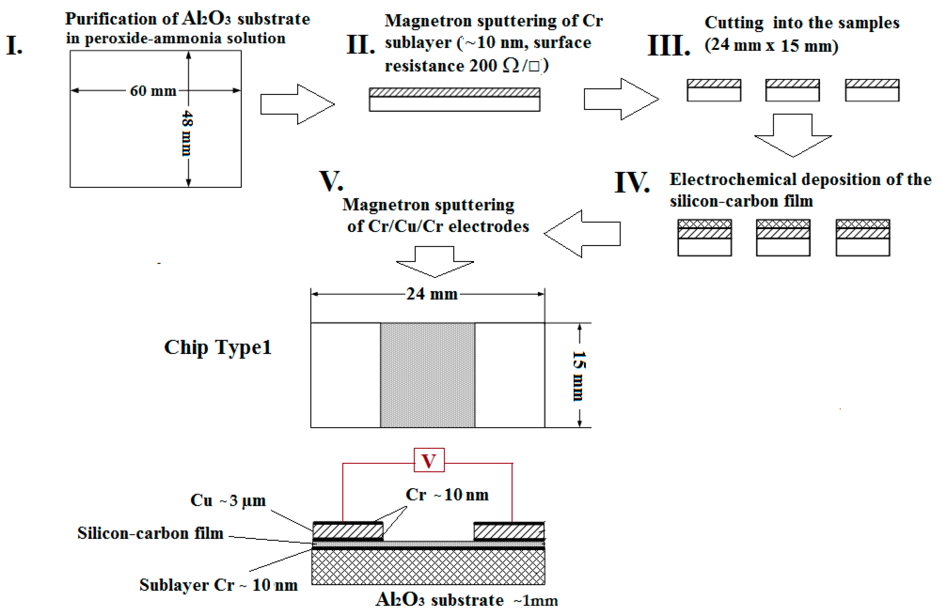
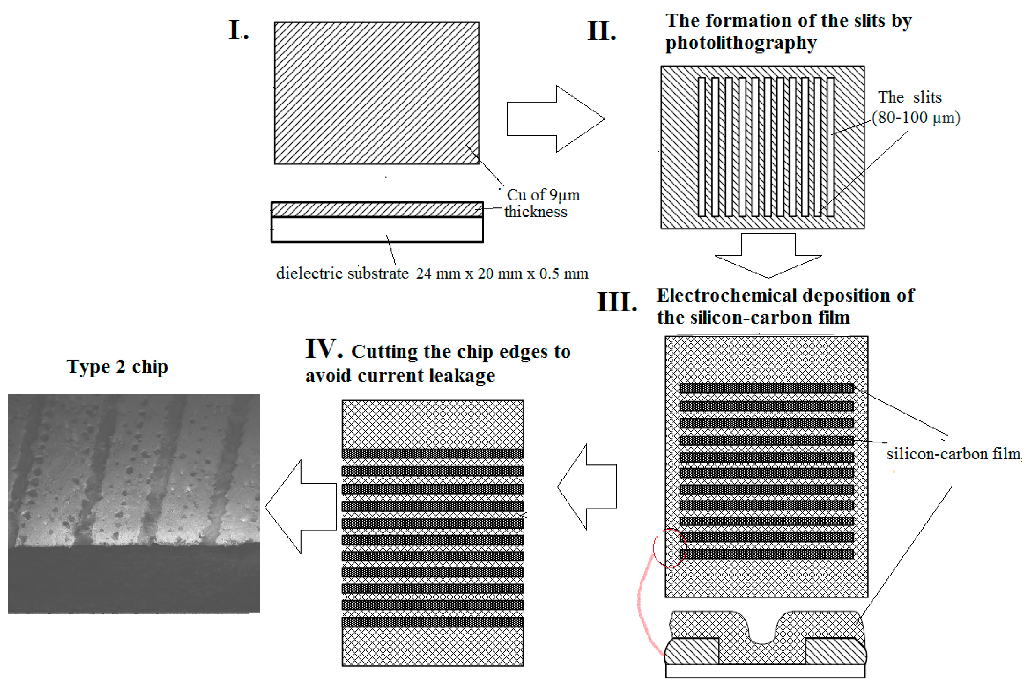
2.3. Fabrication of Gas-Sensor Chips

Two types of gas-sensor chips were designed. The first type of gas-sensor chip (type-1) consisted of an Al2O3 substrate with a conductive chromium sublayer of ~10 nm thickness and 200 Ω/□ surface resistance, deposited by magnetron sputtering. The gas-sensitive silicon–carbon film was electrochemically deposited onto the chromium surface. Finally, the contact electrodes (Cr–Cu–Cr) were sputtered onto the gas-sensitive layer (Figure 1). The presence of a chromium layer at the bottom of the electrode promotes better adhesion of the copper metal, and prevents oxidation of the copper electrode, being on the top.
For the second sensor, a dielectric substrate with a 9 µm-thick copper layer was used. Slits of 80–100 µm width were formed on the surface using the photolytography technique (Figure 2) to design a resistor under the gas-sensitive layer. The silicon–carbon film was deposited onto the surface and the slits were completely overgrown (type-2). Finally, the chip edges were cut to avoid current leakage.
The main process steps are outlined in Figure 1 and Figure 2.
The fabrication of these two types of gas sensor chips allowed us to investigate the effect of the electrode configuration on the sensor characteristics. Differences in metal sublayers influence the film structure and morphology as the main factors of gas adsorption.

2.4. Fabrication of the Silicon–Carbon Film

An electrolytic deposition system was used to obtain silicon–carbon films. It was substantiated and shown in [25]. The substrates were mounted on the negative electrode. A graphite sheet was used as the anode and was separated from the substrate acting as a cathode by ~10 mm.
The deposition was completed in two stages. In the first stage, the pure silicon–carbon film was deposited from a methanol and hexamethyldisilazane (HMDSN) (ratio 9:1) solution. The deposition time depended on the type of substrate: 30 min and 4 h for the type-1 and -2 chips, respectively. The longer deposition time for the type-2 chip was due to the prolonged process of slits overgrowth by the silicon–carbon film. In the second stage, the 0.14 wt% of copper acetate (0.05 wt% of Cu) was added into the methanol and HMDSN solution, and the film deposition was continued for 7–10 min. The deposition potential of pure films was 55 and 75 V for type-1 and -2 chips, respectively, whereas the deposition of the copper acetate-containing solution occurred at ~25 V.

3. Results and Discussion

3.1. Film Characterization

The film thickness estimated by interferometer spectrometry was about 500 nm and 3–4 µm for the films deposited on the type-1 and -2 chips, respectively.
Experimental evidence shows that most materials that can be deposited from the vapor phase can also be deposited in the liquid phase using electrochemical techniques, and vice versa [16,26]. To improve the possibility of the formation of Si–C bonds as a result of the electrochemical deposition of silicon–carbon film from the organic solution, Raman spectroscopy was employed. The Raman spectra contained lines that are characteristic of SiC polytypes. Both samples were characterized by the presence of the hexagonal 6H SiC polytype with impurities of the rhombohedral 15R SiC phase. We observed bands attributed to Si–C bonds at 580.62 cm–1 and 620.9 cm–1 for the films deposited onto the type-1 and -2 chips, respectively.
The appearance of two peaks within wave numbers 1000–1700 cm–1 is characteristic of carbon clusters (G: 1500–1600 cm–1 and D: 1330–1350 cm–1).
Figure 3 shows that the D band was observed in both Raman spectra, whereas the G band was observed only in spectra for the film on the type-2 chip at ~1586 cm−1. A G band represents sp2 bonds, corresponding to those observed in graphite. A D band was observed at ~1339 (type-1) and 1342.27 (type-2) cm−1, which was at a lower wavenumber than the G band, and represents sp3 bonds, corresponding to those observed in diamond [27]. The peaks at 1196 and 1185.6 cm−1 are inferred to be nanocrystalline diamond and sp3 bonds [28].
The ratio of the intensity of the D peak to the G peak (ID/IG) is related to the cluster diameter of the free carbon domains [29]. A smaller ratio corresponds to smaller free carbon clusters. The ID/IG ratio for the film on the type-2 chip was 0.92.
The intensities of the D and G bands of the silicon–carbon film on the type-1 chip were higher than those of the film deposited on the type-2 chip. The high intensity of the D band confirms the existence of unsaturated hydrocarbons on the surface of SiC nanoparticles [30].
The phase formation and surface crystallization were analyzed using XRD, as shown in Figure 4. Copper existed mainly in the CuO state. The XRD data for type-2 gas sensor reveals the intensive peaks for the Cu phase, due to the effect of the copper sublayer on the substrate. So, the copper spontaneously oxidized during the deposition process at 25 V.
SEM analyses were conducted to investigate the surface morphology of the films. Typical SEM micrographs of the pure and CuO alloy silicon–carbon films are shown in Figure 5a–d,f, respectively. The morphology of the as-deposited pure film on the type-1 chip was scaly, whereas the that on the type-2 chip was represented by small and compact grains with an average size of 90 to 130 nm.
The film doped with copper oxide and deposited onto the type-1 chip had a uniformly spherical morphology with an average diameter of about 2 µm. The cross-sectional micrograph in Figure 5e revealed silicon–carbon microspheres covered with copper oxide.
In the case of the copper alloy silicon–carbon film on the type-2 chip, the SEM micrograph (Figure 5d,f) revealed a compact film with well-dispersed nanocrystalline copper in the silicon–carbon matrix.

3.2. Current-Voltage Measurements

Figure 6 depicts the linear current-voltage (I–V) characteristics of the silicon-carbon gas sensors, indicating the establishment of ohmic contact between the gas-sensitive film and the electrodes. The ohmic contact between the metal electrodes and the silicon-carbon film can prevent harmful effects from occurring in the gas sensor. This contact structure not only improves the sensitivity of gas sensors, but also decreases the scatter-in gas-response properties of these sensors.

3.3. Gas-Sensor Characteristics with CH4 and CO Gases

The objective of this investigation was to detect the effect of copper in a silicon–carbon matrix on gas sensing behavior and to compare the different gas-sensor chips fabricated in this work (type-1 and type-2).
The as-developed sensors demonstrated high stability of the surface resistance at operating temperatures. The typical dynamic responses of the different sensor types at 200 °C are shown in Figure 7. The responses are rather low, but stable. The lower the gas concentration, the smaller the signal-to-noise ratio for sensor responses to gas. The sensitivity threshold is usually set to a signal-to-noise ratio of three [31], which was taken as the minimum ratio to determine the response. In pure films, the response is weak; therefore, the noise is more noticeable in Figure 7a,c, since the scale is presented on a narrower range of resistance.
The type-1 sensor demonstrated p-type conductivity (Figure 7a,b) whereas type-2 demonstrated n-type conductivity at operating temperatures above 150 °C (Figure 7c,d). The long deposition time (i.e., four hours) of the silicon–carbon film contributed to a greater increase in the proportion of ordered inclusions of SiC (mostly 6H SiC polytype), through which n-type conductivity was activated by temperature [32].
The operating temperature has a crucial effect on the sensing properties of the gas sensor [33]. Many of metal-oxides or SiC-based gas sensors operate at high temperatures up to 600 °C, and typically encounter many challenging issues, such as thermal and long-term stability, sensitivity, reproducibility, and selectivity. So, the development of sensing materials with good thermal stability and sensing performance is an important task. Figure 8 shows the responses of type-1 and -2 gas sensors to 16 ppm carbon oxide and 297 ppm methane under different temperatures. The type-1 gas sensor presented a volcanic type gas response curve with operating temperature, due to the equilibrium between the resistance drop induced by increasing temperature and a resistance rise resulting from chemisorption of oxygen molecules [32]. The maximum gas response appeared at 200 °C for the type-1 sensors based on the pure film and copper oxide doped film. For the type-2 sensor, the maximum gas response was observed at 250 °C, i.e., larger than that of the type-1 sensor toward CO and CH4 molecules. The further increase in operating temperature is undesirable, as it could lead to carbon graphitization. Both type-1 and -2 gas sensors demonstrated a better gas response to CO, which can be attributed to the presence of the unshared pair of electrons in carbon and oxygen which provides the opportunity to establish additional contacts with the surface.
The sensors based on the pure silicon–carbon film had a poor gas response. The copper oxide introduction into the silicon–carbon matrix increased gas sensor response by six to seven times for both type-1 and -2 sensors (Figure 7). The response and recovery times were 22–33 s and 34–36 s, respectively for the sensors based on the pure silicon–carbon films. The type-1 sensor based on the silicon–carbon/CuO film had a response time of 32–35 s and recovery time of 50–52 s. We observed large differences in the response (600–700 s) and recovery (1226–1233 s) times for the type-2 chip with silicon–carbon/CuO film. The gas diffusion process to adsorption centers is difficult, due to the developed surface morphology of the film (Figure 5d,f).
Figure 9 illustrates the relationship between the gas sensor response and CO and CH4 gas concentration in the range of 8–350 ppm. It was shown that saturation occurs at a CO concentration above 100 ppm. The detection threshold of CO is 16 and 8 ppm for the type-1 and -2 sensors, respectively, while the detection threshold of CH4 gas is 30 ppm.
Another important criterion for gas sensors is selectivity, which is commonly described as the capability of a sensor to differentiate amongst various types of target gases. Hence, the responses of type-1 and -2 sensors to 16 ppm CO, CH4, C2H5OH, NO2, and NH3 gases were measured; the findings are presented in Figure 10. The response of the type-2 sensor to CO was more than two times higher than that of other gases, indicating the substantial selectivity. No response was observed to NO2 gas. The type-1 sensor showed only a small response to CO gas.
The sensor’s resistance was examined to air humidity at room temperature. The results are presented in Table S1.
Table 1 provides detailed data of different CuO-based gas sensors. The sensors are sensitive to different gases (CO2, CO, C2H4O, H2S, C2H5OH, NH3, CH4, C3H6). The response and recovery time, as important parameters by which to evaluate the performance of a gas sensor, vary from 8 s to 15 min and 5 s to 50 min, respectively. The operating temperatures of sensors in most cases reach 200–500 °C. Thus, we can conclude that our sensors are not inferior in their characteristics to others reported in the literature. Also, sensors of both type-1 and -2 detect CO at a concentration of 16 ppm, while well-known CuO-based sensors determine concentrations of at least 200 [36] and 2000 [45] ppm. Only one source [50] reported a CuO sensor for 10,000 ppm CH4 detection at 300 °C, while our sensors detect 297 ppm of methane at 200 °C.

3.4. Conductivity Investigation

3.4.1. Conductivity Mechanism

The Raman spectroscopy data showed that the films are heterogeneous, with inclusions of sp2 and sp3 carbon and silicon carbide (amorphous and crystallite) phases being responsible for the conductivity type.
The films doped with copper also are characterized by the presence of copper oxide. The sp2/sp3 ratio is responsible for the conductivity in pure silicon-carbon materials [51].
The conductivity of semiconductors is due to the concentration of charge carriers and their mobility. Inside the regions of different phases and on the border between them, various mechanisms of conductivity are possible: tunneling, hopping, and percolation [52].
The resistance (R) dependence on temperature (T); (LnR–1/T coordinates) (Figure 11) revealed two areas that are responsible for the predominance of a conductivity mechanism, which is typical for composite materials (hopping mechanism) and may be associated with a mismatch in the coefficients of thermal expansion of the constituent parts of the material structure [53]. In composite films, when the temperature increases, the interaction of copper oxide with the crystalline lattice of silicon carbide leads to the appearance of bond breaks, and the formation of the density of localized states occurs. In the case of the hopping mechanism, the electrical conductivity increases [54]. The response to gases was observed at temperatures of 150 °C and above.
A slight change in resistance with increasing temperature in sensors based on pure silicon–carbon films indicates the structural disorder of the material and the absence of a significant effect of the metal sublayer. The low mobility of charge carriers is the possible reason for the poor sensitivity of pure silicon–carbon samples.
A slight decrease in resistance change with the introduction of copper indicates a weak degree of doping of the material. The resistance decreases by 10 and 27 times with copper oxide introduction for type-1 and -2 gas sensors, respectively. The distribution of conductive particles in the film on the type-2 chip is more uniform, which contributes to hopping conductivity, but the percolation threshold is not reached and the percolation conduction mechanism does not work [55].
The presence of the sp3 carbon phase and the silicon carbide phase creates bond breaks on the surface of the film which are temporarily occupied by hydrogen. C–H bonds break with increasing temperature and the molecules of gases use the bond break as adsorption centers. The adsorption centers for reducing gases are copper oxide particles:
CH4 → CH4+ + ē
CO → CO+ + ē
The better response to CO is explained by the adsorbed oxygen [56]:
2CO + O2- → CO2 + ē
CuO in such interactions plays the role of catalyst.

3.4.2. Type of Conductivity (Mott-Shottki Plot)

During the gas sensing test, a p- and n-type of conductivity was found for type-1 and -2 gas sensors, respectively, at operating temperatures above 150 °C. To understand the semiconductor characteristics of the composite film, a Mott−Schottky analysis in 3.5 M KOH was performed; the results are presented in Figure 12. The sensors show the presence of both positive (p) and negative (n) slopes in the linear region of the Mott–Schottky plot, attributed to the presence of p- and n-type phases [57]. The negative slopes (n) of both types of gas sensors are found to be lower, whereas the positive slopes for p-type are higher, which implies the low carrier density and poor conductivity of the n-type region [58]. Thus, we suppose that both the type-1 and -2 gas sensors demonstrate p-type conductivity at room temperature.
Since our testing gases (CH4 and CO) are reducing type, the gas molecules should provide electrons, when adsorbed on the surface of the p-type film, resulting in an increase of resistance. However, the dynamic response curves (Figure 7) of the type-2 sensor show n-type characteristics at 200 °C, which suggests that the conductivity of the silicon-carbon sensor may be changed when it is heated. This fact may be explained by the silicon-carbon film structure formed due to the technological conditions of electrochemical deposition. Raman spectroscopy (Figure 3) data reveals a greater extent to the share of ordered n-type 6H SiC and graphite phases, the conductivity of which is activated by temperature [31].

4. Conclusions

In this study, we fabricated two types of gas sensors based on silicon-carbon films. The silicon-carbon films were electrochemically deposited via a two-stage technique onto an Al2O3 substrate with a chromium sublayer and onto a dielectric substrate with copper electrodes with a special configuration. The electrochemical sensors made possible the direct synthesis of the sensing layer on the substrate, which improved the sensitivity. The films were characterized by Raman spectroscopy and XRD analysis.
The gas sensitivity of the chips for CO and CH4 gases was examined. The sensors based on the pure silicon-carbon film had a poor gas response. Copper introduction into the silicon-carbon matrix increased gas sensor response by six to seven times. The type-1 sensor demonstrated p-type conductivity, whereas the type-2 sensor demonstrated n-type conductivity, at operating temperatures above 150 °C.
A response investigation of type-1 and -2 sensors to 16 ppm CO, CH4, C2H5OH, NO2, and NH3 gases showed that the response of the type-2 sensor to CO was more than two times higher than other gases, indicating substantial selectivity. The type-1 sensor showed only a small response to CO gas.
The type-1 gas sensor showed fast response and recovery time but low sensitivity, while the type-2 sensor was characterized by high sensitivity but longer response and recovery time.
We showed that the design of the sensor chip can strongly effect the sensitivity of the gas sensor.

Supplementary Materials

The following are available online at https://www.mdpi.com/2227-9040/7/4/52/s1, Table S1: Effect of air humidity on resistance drift at room temperature.

Author Contributions

Conceptualization, T.N.M. and N.K.P.; data curation, T.N.M. and N.K.P.; formal analysis, T.N.M. and N.K.P.; funding acquisition, T.N.M. and N.K.P.; investigation, M.N.G. and T.S.M.; methodology, T.N.M., M.N.G., and N.K.P.; project administration, T.N.M. and N.K.P.; resources, T.N.M., M.N.G., and N.K.P.; software, N.K.P.; supervision, T.N.M.; validation, T.N.M. and N.K.P.; visualization, T.N.M., M.N.G., N.K.P., and T.S.M.; writing-original draft preparation, T.N.M.; writing-article and editing, T.N.M. and T.S.M.

Funding

This work was financially supported by the Ministry of Education of Russia, under Contract No. 14.575.21.0126 (the unique identifier of the contract is RFMEFI57517X0126).

Acknowledgments

The authors acknowledge the Center for collective use of Microsystem Technology and Integrated sensorics (Southern Federal University, Taganrog, Russia) for the gas sensitivity experiments, and the Center for collective use of scientific equipment of the North-Caucasus Federal University (Stavropol, Russia) for Raman spectroscopy investigations.

Conflicts of Interest

The authors declare no conflict of interest. The funders had no role in the design of the study in the collection, analyses, or interpretation of data; in the writing of the manuscript; or in the decision to publish the results.

References

  1. Nebel, M.; Neugebauer, S.; Kiesele, H.; Schuhmann, W. Local reactivity of diamond-like carbon modified PTFE membranes used in SO2 sensors. Electrochim. Acta 2010, 55, 7923–7928. [Google Scholar] [CrossRef]
  2. Korotcenkov, G. Gas response control through structural and chemical modification of metal oxide films: State of the art and approaches. Sens. Actuators B Chem. 2005, 107, 209–232. [Google Scholar] [CrossRef]
  3. Myasoedova, T.N.; Mikhailova, T.S.; Yalovega, G.E.; Plugotarenko, N.K. Resistive low-temperature sensor based on the SiO2ZrO2 film for detection of high concentrations of NO2 gas. Chemosensors 2018, 6, 67. [Google Scholar] [CrossRef]
  4. Zhang, C.; Luo, Y.; Xu, J.; Debliquy, M. Room temperature conductive type metal oxide semiconductor gas sensors for NO2 detection. Sens. Actuators A Phys. 2019, 289, 118–133. [Google Scholar] [CrossRef]
  5. Khodadadi, A.; Mohajerzadeh, S.S.; Mortazavi, Y.; Miri, A.M. Cerium oxide/SnO2-based semiconductor gas sensors with improved sensitivity to CO. Sens. Actuators B Chem. 2001, 80, 267–271. [Google Scholar] [CrossRef]
  6. Markwitz, A.; Leveneur, J.; Gupta, P.; Suschke, K.; Futter, J.; Rondeau, M. Transition metal ion implantation into diamond-like carbon coatings: Development of a base material for gas sensing applications. J. Nanomater. 2015, 16, 50. [Google Scholar] [CrossRef]
  7. Bhadra, N.; Hussain, S.; Das, S.; Bhunia, R.; Bhar, R.; Pal, A.K. H2S gas sensor based on nanocrystalline copper/dlc composite films. Plasmonics 2015, 10, 503–509. [Google Scholar] [CrossRef]
  8. Presniakov, M.Y.; Popov, A.I.; Shupegin, M.L.; Usoltseva, D.S.; Vasiliev, A.L. Thermal stability of metal-silicon–carbon nanocomposites. Nanotechnol. Russ. 2014, 9, 518–532. [Google Scholar] [CrossRef]
  9. Yang, W.J.; Choab, Y.H.; Sekinoc, T.; Shima, K.B.; Niiharac, K.; Auha, K.H. Thermal stability evaluation of diamond-like nanocomposite coatings. Thin Solid Films 2003, 434, 49–54. [Google Scholar] [CrossRef]
  10. Choi, H.W.; Choi, J.-H.; Lee, K.-R.; Ahn, J.-P.; Oh, K.H. Structure and mechanical properties of Ag-incorporated DLC films prepared by a hybrid ion beam deposition system. Thin Solid Films 2007, 516, 248–251. [Google Scholar] [CrossRef]
  11. Ohno, T.; Takeno, T.; Miki, H.; Takagi, T. Microstructural design for fabrication of strain sensor utilizing tungsten-doped amorphous carbon coatings. Diam. Relat. Mater. 2011, 20, 651–654. [Google Scholar] [CrossRef]
  12. Koh, A.T.T.; Hsieh, J.; Chua, D.H.C. Structural characterization of dual-metal containing diamond-like carbon nanocomposite films by pulsed laser deposition. Diam. Relat. Mater. 2010, 19, 637–642. [Google Scholar] [CrossRef]
  13. Kosukegawa, H.; Berkani, S.; Miki, H.; Takagi, T. Structure and electrical properties of molybdenum-containing diamond-like carbon coatings for use as fatigue sensors. Diam. Relat. Mater. 2017, 80, 38–44. [Google Scholar] [CrossRef]
  14. Falcade, T.; Shmitzhaus, T.E.; dos Reis, O.G.; Vargas, A.L.M.; Hubler, R.; Muller, I.L.; de Fraga, M.C. Electrodeposition of diamond-like carbon films on titanium alloy using organic liquids: Corrosion and wear resistance. Appl. Surf. Sci. 2012, 263, 18–24. [Google Scholar] [CrossRef] [Green Version]
  15. Yan, X.B.; Xu, T.; Chen, G.; Xue, Q.J.; Yang, S.R. Synthesis of diamond-like carbon/nanosilica composite films by an electrochemical method. Electrochem. Commun. 2004, 6, 1159–1162. [Google Scholar] [CrossRef]
  16. Wang, H.; Shen, M.R.; Ning, Z.Y.; Cao, C.B.; Dang, H.Y.; Zhu, H.S. Deposition of diamond-like carbon films by electrolysis of methanol solution. Appl. Phys. Lett. 1996, 69, 1074–1076. [Google Scholar] [CrossRef]
  17. Cai, K.; Cao, C.B.; Zhu, H.S. Deposition of diamond-like carbon films on aluminium in the liquid phase by an electrochemical method. Carbon 1999, 37, 1860–1862. [Google Scholar] [CrossRef]
  18. Guo, D.; Cai, K.; Li, L.T.; Huang, Y.; Gui, Z.L.; Zhu, H.S. Evaluation of diamond-like carbon films electrodeposited on an Al substrate from the liquid phase with pulse-modulated power. Carbon 2001, 39, 1395–1398. [Google Scholar] [CrossRef]
  19. Kulak, A.I.; Kokorin, A.I.; Meissner, D.; Ralchenko, V.G.; Vlasov, I.I.; Kondratyuk, A.V.; Kulak, T.I. Electrodeposition of nanostructured diamond-like films by oxidation of lithium acetylide. Electrochem. Commun. 2003, 5, 301–305. [Google Scholar] [CrossRef]
  20. Yunusa, Z.; Hamidon, M.N.; Kaiser, A.; Awang, Z. Gas Sensors: A Review. Sens. Transducers 2014, 168, 61–75. [Google Scholar]
  21. Yalovega, G.E.; Myasoedova, T.N.; Funik, A.O.; Plugotarenko, N.K.; Brzhezinskaya, M.; Bahmatskaya, A.I. Mechanism of the formation of copper-containing fractal-like crystallites in metal-organic thin films: Shape simulation and XANES analysis. Phys. Status Solidi B 2016, 253, 2217–2224. [Google Scholar] [CrossRef]
  22. Tsai, C.-H.; Fei, P.-H.; Lin, C.-M.; Shiu, S.-L. CuO and CuO/graphene nanostructured thin films as counter electrodes for Pt-free dye-sensitized solar cells. Coatings 2018, 8, 21. [Google Scholar] [CrossRef]
  23. Rydosz, A. The use of copper oxide thin films in gas-sensing applications. Coatings 2018, 8, 425. [Google Scholar] [CrossRef]
  24. Myasoedova, T.N.; Yalovega, G.E.; Shmatko, V.A.; Funik, A.O.; Petrov, V.V. SiO2CuOx films for nitrogen dioxide detection: Correlation between technological conditions and properties. Sens. Actuators B Chem. 2016, 230, 167–175. [Google Scholar] [CrossRef]
  25. Grigoryev, M.N.; Myasoedova, T.N.; Mikhailova, T.S. The electrochemical deposition of silicon–carbon thin films from organic solution. J. Phys. Conf. Ser. 2018, 1124, 081043. [Google Scholar] [CrossRef]
  26. Maissel, L.L.; Glang, R. Handbook of Thin Film Technology; McGraw-Hill: New York, NY, USA, 1970; Chapter 5; p. 5. [Google Scholar]
  27. Ferrari, A.C.; Robertson, J. Raman spectroscopy of amorphous, nanostructured, diamond-like carbon, and nanodiamond. Philos. Trans. R. Soc. Lond. A 2004, 362, 2477–2512. [Google Scholar] [CrossRef]
  28. Chu, P.K.; Li, L. Characterization of amorphous and nanocrystalline carbon films. Mater. Chem. Phys 2006, 96, 253–277. [Google Scholar] [CrossRef]
  29. Mehr, M.; Moore, D.T.; Esquivel-Elizondo, J.R.; Nino, J.C. Mechanical and thermal properties of low temperature sintered silicon carbide using a preceramic polymer as binder. J. Mater. Sci. 2015, 50, 7000–7009. [Google Scholar] [CrossRef]
  30. Iijima, M.; Kamiya, H. Surface modification of silicon carbide nanoparticles by Azo Radical Initiators. J. Phys. Chem. C 2008, 112, 11786–11790. [Google Scholar] [CrossRef]
  31. Ren, M.; Kang, X.; Li, L.; Duan, L.; Liao, F. Electrochemical sensor based on Ni/reduced graphene oxide nanohybrids for selective detection of ascorbic acid. J. Dispers. Sci. Technol. 2019. [Google Scholar] [CrossRef]
  32. Dinh, T.; Dao, D.V.; Phan, H.-P.; Wang, L.; Qamar, A.; Nguyen, N.-T.; Tanner, P.; Rybachuk, M. Charge transport and activation energy of amorphous silicon carbide thin film on quartz at elevated temperature. Appl. Phys. Express 2015, 8, 061303. [Google Scholar] [CrossRef]
  33. Li, N.; Fan, Y.; Shi, Y.; Xiang, Q.; Wang, X.; Xu, J. A low temperature formaldehyde gas sensor based on hierarchical SnO/SnO2 nano-flowers assembled from ultrathin nanosheets: Synthesis, sensing performance and mechanism. Sens. Actuators B Chem. 2019, 294, 106–115. [Google Scholar] [CrossRef]
  34. Wimmer-Teubenbacher, R.; Sosada-Ludwikowska, F.; Zaragoza Travieso, B.; Defregger, S.; Tokmak, O.; Niehaus, J.S.; Deluca, M.; Köck, A. CuO thin films functionalized with gold nanoparticles for conductometric carbon dioxide gas sensing. Chemosensors 2018, 6, 56. [Google Scholar] [CrossRef]
  35. Rydosz, A.; Szkudlarek, A. Gas-sensing performance of M-Doped CuO-based thin films working at different temperatures upon exposure to propane. Sensors 2015, 15, 20069–20085. [Google Scholar] [CrossRef]
  36. Presmanes, L.; Thimont, Y.; el Younsi, I.; Chapelle, A.; Blanc, F.; Talhi, C.; Bonningue, C.; Barnabé, A.; Menini, P.; Tailhades, P. Integration of P-CuO thin sputtered layers onto microsensor platforms for gas sensing. Sensors 2017, 17, 1409. [Google Scholar] [CrossRef]
  37. Li, D.; Tang, Y.; Ao, D.; Xiang, X.; Wang, S.; Zu, H. Ultra-highly sensitive and selective H2S gas sensor based on CuO with sub-ppb detection limit. Int. J. Hydrogen Energy 2019, 44, 3985–3992. [Google Scholar] [CrossRef]
  38. Lee, J.E.; Do Kim, Y.; Lee, H.-K.; Park, H.J.; Mab, A.; Choi, S.-Y.; Lee, D.-S. Sonochemical synthesis of HKUST-1-based CuO decorated with Pt nanoparticles for formaldehyde gas-sensor applications. Sens. Actuators B Chem. 2019, 292, 289–296. [Google Scholar] [CrossRef]
  39. Hou, L.; Zhang, C.; Li, L.; Du, C.; Li, X.; Kang, X.-F.; Chen, W. CO gas sensors based on p-type CuO nanotubes and CuO nanocubes: Morphology and surface structure effects on the sensing performance. Talanta 2018, 188, 41–49. [Google Scholar] [CrossRef]
  40. Li, D.; Zu, X.; Ao, D.; Tang, Q.; Fu, Y.; Guo, Y.; Bilawal, K.; Faheem, M.B.; Li, L.; Li, S.; et al. High humidity enhanced surface acoustic wave (SAW) H2S sensors based on sol–gel CuO films. Sens. Actuators B Chem. 2019, 294, 55–61. [Google Scholar] [CrossRef]
  41. Sarıca, N.; Alev, O.; Arslan, L.Ç.; Öztürk, Z.Z. Characterization and gas sensing performances of noble metals decorated CuO nanorods. Thin Solid Films 2019, 685, 321–328. [Google Scholar] [CrossRef]
  42. Poloju, M.; Jayababu, N.; Reddy, M.V.R. Improved gas sensing performance of Al doped ZnO/CuO nanocomposite based ammonia gas sensor. Mater. Sci. Eng. B 2018, 227, 61–67. [Google Scholar] [CrossRef]
  43. Han, C.; Chen, X.; Liu, D.; Zhou, P.; Zhao, S.; Bi, H.; Meng, D.; Wei, D.; Shen, Y. Fabrication of shrub-like CuO porous films by a top-down method for highperformance ethanol gas sensor. Vacuum 2018, 157, 332–339. [Google Scholar] [CrossRef]
  44. Park, H.J.; Choi, N.-G.; Kang, H.; Jung, M.Y.; Park, J.W.; Park, K.H.; Lee, D.-S. A ppb-level formaldehyde gas sensor based on CuO nanocubes prepared using a polyol process. Sens. Actuators B Chem. 2014, 203, 282–288. [Google Scholar] [CrossRef]
  45. Javanmardi, S.; Nasresfahani, S.; Sheikhi, M.H. Facile synthesis of PdO/SnO2/CuO nanocomposite with enhanced carbon monoxide gas sensing performance at low operating temperature. Mater. Res. Bull. 2019, 118, 110496. [Google Scholar] [CrossRef]
  46. Xu, H.; Zhu, Z.; Chen, C.; Wen, T.; Zhao, X.; Xie, L. Highly sensitive H2S gas sensors based on Pd-doped CuO nanoflowers with low operating temperature. Sens. Actuators B Chem. 2017, 253, 809–817. [Google Scholar]
  47. Behera, B.; Chandra, S. An innovative gas sensor incorporating ZnO-CuO nanoflakes in planar MEMS technology. Sens. Actuators B Chem. 2016, 229, 414–424. [Google Scholar] [CrossRef]
  48. Umar, A.; Alshahrani, A.A.; Angarni, H.; Kumar, R. CuO nanosheets as potential scaffolds for gas sensing applications. Sens. Actuators B Chem. 2017, 250, 24–31. [Google Scholar] [CrossRef]
  49. Park, S.; Kim, S.; Kheel, H.; Hyun, S.K.; Jin, S.; Lee, C. Enhanced H2S gas sensing performance of networked CuO-ZnO composite nanoparticle sensor. Mater. Res. Bull. 2016, 82, 130–135. [Google Scholar] [CrossRef]
  50. Shaalan, N.M.; Rashad, M.; Abdel-Rahim, M.A. CuO nanoparticles synthesized by microwave-assisted method for methane sensing. Opt. Quantum Electron. 2016, 48, 531. [Google Scholar] [CrossRef]
  51. Wong, H.; Foong, Y.M.; Chua, D.H.C. Improving the conductivity of diamond-like carbon films with zinc doping and its material properties. Appl. Surf. Sci. 2011, 257, 9616–9620. [Google Scholar] [CrossRef]
  52. Konezny, S.J.; Bussac, M.N.; Geiser, A.; Zuppiroli, L. Charge transport mechanisms in organic and microcrystalline silicon field-effect transistors. Proc. SPIE 2007, 6658, 66580D. [Google Scholar]
  53. Wang, W.; Wang, C.; Yue, X.; Zhang, C.; Zhou, C.; Wu, W.; Zhu, H. Raman spectroscopy and resistance-temperature studies of functionalized multiwalled carbon nanotubes/epoxy resin composite film. Microelectron. Eng. 2019, 214, 50–54. [Google Scholar] [CrossRef]
  54. Barinov, A.D.; Popov, A.I.; Presnyakov, Y.M. Effect of nanophase concentration on the properties of metal-containing silicon–carbon nanocomposites. Inorg. Mater. 2017, 53, 690–696. [Google Scholar] [CrossRef]
  55. Zav’yalova, S.A.; Kupriyanova, L.Y.; Pivkinab, A.N.; Shounman, J. The microstructure of and charge transfer in thin films based on metal–polymer nanocomposites. Russ. J. Phys. Chem. 2006, 80, 1461–1466. [Google Scholar] [CrossRef]
  56. Sun, L.; Han, C.; Wu, N.; Wang, B.; Wang, Y. High temperature gas sensing performances of silicon carbide nanosheets with an n–p conductivity transition. RSC Adv. 2018, 8, 13697–13707. [Google Scholar] [CrossRef]
  57. Swain, G.; Sultana, S.; Naik, B.; Parida, K. Coupling of crumpled-type novel MoS2 with CeO2 nanoparticles: A noble-metal-free p–n heterojunction composite for visible light photocatalytic H2 production. ACS Omega 2017, 2, 3745–3753. [Google Scholar] [CrossRef] [PubMed]
  58. Liu, Y.; Yu, Y.-X.; Zhang, W.-D. MoS2/CdS heterojunction with high photoelectrochemical activity for H2 evolution under visible light: The role of MoS2. J. Phys. Chem. C 2013, 117, 12949–12957. [Google Scholar] [CrossRef]
Figure 1. General sensor fabrication process on an Al2O3 substrate with a chromium sublayer (type-1).
Chemosensors 07 00052 g001
Figure 2. General sensor fabrication process on a dielectric substrate with copper electrodes (type-2).
Chemosensors 07 00052 g002
Figure 3. Raman spectra of the pure silicon–carbon films. ND denotes nanocrystalline diamond.
Chemosensors 07 00052 g003
Figure 4. XRD of silicon–carbon films, doped with copper.
Chemosensors 07 00052 g004
Figure 5. SEM micrographs of silicon-carbon films: (a) pure film on the type-1 chip; (b) film doped with CuO on the type-1 chip; (c) pure film on the type-2 chip; (d) film doped with CuO on the type-2 chip; and cross-sections of the (e) type-1 and (f) type-2 chips with the CuO alloy silicon-carbon film.
Chemosensors 07 00052 g005aChemosensors 07 00052 g005b
Figure 6. Current–voltage (I–V) curves of the gas sensor chips based on the silicon–carbon film, doped with Cu: (a) type-1 and (b) type-2 chips.
Chemosensors 07 00052 g006
Figure 7. Typical dynamic response of the (a,b) type-1 and (c,d) type-2 sensors toward 16 ppm CO and 297 ppm CH4 at 200 °C. Grey represents gas inputs.
Chemosensors 07 00052 g007aChemosensors 07 00052 g007b
Figure 8. Relationship between the response and the optimal operating temperature of the sensors to 16 ppm CO and 297 ppm CH4 for films: (a) type-1 and (b) type-2 chips.
Chemosensors 07 00052 g008
Figure 9. Relationship between the response and CO (a,d) and CH4 (c,d) concentration for type-1 (film, doped with CuO) (a,b) and type-2 (film, doped with CuO) (c,d)) gas sensor at 200 °C (type-1) and 250 °C (type-2).
Chemosensors 07 00052 g009
Figure 10. Sensors response towards 16 ppm of different gases at 200 °C (type-1 (film, doped with CuO) and 250 °C (type-2 (film, doped with CuO)).
Chemosensors 07 00052 g010
Figure 11. Dependence of ln(R) on the 1/T or the gas sensor chips: (a) type-1 and (b) type-2. R denotes resistance, T denotes temperature.
Chemosensors 07 00052 g011
Figure 12. Mott‒Schottky plots for type-1 and -2 sensors under different applied potentials.
Chemosensors 07 00052 g012
Table 1. Comparison of reported CuO-based gas sensors fabricated by different methods.
MaterialProduction MethodDetectable Gases (Detection Limit)Operation Temperature, °CResponse TimeRecovery TimeReference
Au-NPs (gold nanopartic-les) functionalized CuOThermal oxidationCO2 (2000 ppm)3004.3 min4.4 min[34]
CO (200 ppm)3 min10 min
Cr-doped CuO thin filmsMagnetron sputteringC3H8 (100 ppm)25010 s24 s[35]
p-type CuORadio-frequency sputteringC2H4O (5 ppm)40015 min30 min[36]
CO (200 ppm)15 min30 min
CuOMethod combining a hydrothermal reducing process and a thermal oxidation process; dip-coating method of forming a gas sensorH2S (1000 ppb)20200 s1000 s[37]
CuO+Pt NPsSonochemical synthesis methodHCHO (1 ppm)225--[38]
CuO nanotubesOxidation of copper nanowires at 400–700 °C for 5 hCO (1000 ppm)17529 s37 s[39]
Porous CuOSol-gel processH2S (5 ppm)251500 s3000 s[40]
Pt/CuO nanorodHydrothermal synthesisC2H5OH (1000 ppm)2008 min23 min[41]
Al-ZnO/CuO NCsSol-gel processAmmonia (100 ppm)2514 s9 s[42]
Shrub-like CuO porous filmsChemical etching methodC2H5OH (500 ppm)25052 s42 s[43]
CuO nanocubesPolyol process and thermal oxidation under air conditionsHCHO (3 ppm)350--[44]
(7% PdO)/SnO2/CuO NCsHydrothermal route coupled with multiple thermal processesCO (2000 ppm)20070 s10 s[45]
Pd-doped CuO nsnoflowersWater bath heating methodH2S (50 ppm)8015 s12 s[46]
CuO-ZnO nanoflakesThermal oxidationAcetone (10 ppm)30022 s26 s[47]
CuO NCs with nanosheets morphologiesHydrothermal synthesisCH3OH (100 ppm)37010 s7 s[48]
C2H5OH (100 ppm)15 s11 s
Acetone (100 ppm)14 s5 s
CuO-ZnO composite NPsSolvothermal methodH2S (2 ppm)2253098[49]
CuOMicrowave synthesisCH4 (1000–10000 ppm)300~8 min~2 min[50]
Type 1 (silicon-carbon/CuO)Electrochemical deposition from organic solutionCO
(16ppm) CH4
(297 ppm)
20032–35 s50–52 sThis work
Type 2 (silicon-carbon-CuO)600–7001226–1233

