1. Introduction
Phosphate is an essential nutrient in aquatic ecosystems, however its excessive presence can severely impair water quality [
1]. Maintaining an appropriate phosphate balance is crucial to preventing ecological disturbances and sustaining a healthy aquatic environment [
2], as elevated concentrations are associated with significant environmental and health concerns. Environmentally, excessive phosphate promotes eutrophication [
3], which triggers the overgrowth of algae and aquatic plants, ultimately leading to oxygen depletion and increased toxicity in surface waters [
4]. In addition, elevated phosphate levels in the human body are associated with a range of health disorders, notably hyperphosphatemia [
3], which can lead to severe complications such as chronic kidney disease (CKD), vascular calcification, cardiovascular disease, secondary hyperparathyroidism, and renal osteodystrophy. This associations underscore the critical importance of precise phosphate detection in both environmental monitoring and clinical diagnostics [
4]. Moreover, phosphate accumulation in aquatic systems degrades water quality, fosters the proliferation of harmful algal blooms, and increases fish mortality rates [
5]. According to the United States Environmental Protection Agency (USEPA), eutrophication may occur when phosphate concentrations exceed 10 µg/L [
6]. Consequently, the accurate and efficient detection of phosphate is essential across a broad spectrum of disciplines, including environmental science, biomedical research, analytical chemistry, industrial processes, and agriculture [
7]. Various analytical techniques have been employed for phosphate detection in aquatic environments, including ion chromatography, fluorometry, spectrophotometry [
8], flow injection analysis, and potentiometry [
9]. However, these methods are often expensive, labor-intensive, and generate significant chemical waste. As a result, there is a growing need for the development of simpler, more cost-effective, and highly sensitive and selective technologies for phosphate detection in environmental samples. In this context, electrochemical sensors have emerged as a promising alternative, offering reduced operational costs and enhanced analytical performance.
Silicon nanowires (SiNWs) have emerged as promising tools for electrochemical sensors [
10]. Their unique properties, including a high surface-to-volume ratio and enhanced electron transport resulting from quantum confinement effects, make them excellent candidates for highly sensitive detection applications [
11]. Furthermore, SiNWs can be effectively functionalized with specific target molecules, enabling selective binding to analytes of interest. This synergy between nanomaterials and molecular recognition elements paves the way for the development of highly sensitive and selective sensors for a wide range of applications. This synthesis of SiNWs is a complex and multifaceted scientific challenge, with researchers investigating various fabrication techniques that are generally classified as either bottom-up and top-down approaches. These include methods such as vapor–liquid–solid (VLS), vapor–solid–solid (VSS), laser ablation, and metal-assisted chemical etching (MACE). Among these, MACE has gained significant attention in recent years due to its simplicity, cost-effectiveness, and precise control over key parameters such as nanowire diameter, length, orientation, and doping levels [
12]. Phthalocyanines (Pcs) are a class of macrocyclic compounds that have garnered significant attention due to their exceptional chemical and thermal stability, distinctive optical properties (notably characterized by the Q and B bands), and low solubility [
13]. These macrocycles exhibit unique electronic, optical, and catalytic properties, making them highly effective in enhancing sensor performance, particularly in terms of sensitivity and selectivity toward specific analytes. One of the most valuable features of phthalocyanines is their structural tunability, which can be achieved by modifying the central metal ion or by introducing various axial or peripheral functional groups [
13,
14]. These modifications allow for precise tailoring of their electronic, chemical, and electrochemical characteristics, rendering them highly adaptable for specific sensing applications, including phosphate ion detection. Moreover, phthalocyanines and their metal complexes (MPcs) display strong π–π conjugation, remarkable thermal and chemical stability, and high redox activity, all of which contribute to their excellent performance in sensing platforms [
14]. Their versatility has led to widespread applications in various domains, including solar cells [
15], catalysis [
16], and electrochemical devices [
17]. The ability to coordinate with a broad range of metal ions and to undergo targeted structural modifications further enhances their potential in the development of highly selective and sensitive electrochemical sensors.
In this study, we employed a novel copper (II) phthalocyanine derivative (Cu (II) Pc-PAA), which presents multiple advantages for the development of electrochemical sensors targeting phosphate ion detection. The covalent bonding of Cu (II) Pc-PAA to the polymer matrix offers enhanced long-term stability by preventing ionophore leaching, crystallization, and evaporation [
13]. Furthermore, the specific interaction between phosphate ions and the copper center within the phthalocyanine structure, reinforced by the polymeric environment, contributes to improved sensitivity and selectivity.
We aim to develop an electrochemical sensor based on two advanced materials: silicon nanowires (SiNWs) fabricated via the MACE method and functionalized with a novel copper (II) phthalocyanine derivative (Cu (II) Pc-PAA) for the detection of toxic phosphate pollutants. The MACE technique offers a cost-effective, scalable, and controllable approach for producing SiNWs with high surface area, which significantly enhances the electrochemical performance of the sensor. The combination of these materials enables sensitive and selective phosphate detection, even at trace levels.
Various electrochemical sensors for phosphate detection have been reported such as copper-based electrodes [
18] and Cu
2O nanostructure-based sensors [
19]. They exhibit certain limitations in sensitivity and selectivity when compared to SiNW-based platforms. SiNW-based sensors, particularly when functionalized with copper (II) phthalocyanine derivatives like Cu (II) Pc-PAA, demonstrate superior analytical performance, making them highly promising candidates for practical applications in environmental monitoring and water quality assessment.
2. Materials and Methods
The following chemicals were used in this study: acetone (99.6%), ethanol (99.6%), hydrofluoric acid (HF), hydrogen peroxide (H2O2, 34.6%), silver nitrate (AgNO3), nitric acid (HNO3, 6%), tetrahydrofuran (THF), and dimethyl sulfoxide (DMSO). Sodium hydrogen phosphate (Na2HPO4) and potassium dihydrogen phosphate (KHPO4) were employed to prepare phosphate-buffered saline (PBS) at a concentration of 10 mM and pH 7.2. Sodium hydrogen phosphate, hydrochloric acid, potassium sulfate, potassium nitrate, and lithium perchlorate were used to prepare solutions containing the ions HPO42−, Cl−, SO42−, NO3−, and ClO4−, respectively. A novel copper (II) phthalocyanine derivative, C, C, C, C-tetracarboxylic acid-polyacrylamide (Cu (II) Pc-PAA), was synthesized at the National Research Centre in Cairo, Egypt.
The synthesized Cu (II) Pc-PAA contains a central copper atom and is composed of four isoindole units (each consisting of a benzene ring fused to a pyrrole ring) linked through nitrogen atoms. This nanomaterial exhibits excellent selectivity for phosphate detection [
14]. The compound was characterized by elemental analysis, ultraviolet–visible (UV–Vis) spectroscopy, and infrared (IR) spectroscopy to confirm the formation of both the ionophore copper phthalocyanine-C,C,C,C-tetracarboxylic acid (I) and its polyacrylamide adduct (II). Briefly, the synthesis involved the condensation of trimellitic anhydride in the presence of urea, ammonium molybdate, and copper acetate to yield tetra-amido-phthalocyanine copper. Subsequent hydrolysis of this intermediate under alkaline conditions produced the ionophore (I). The polymer adduct (II) was then synthesized, following a previously reported procedure, by refluxing ionophore (I) with polyacrylamide in dimethylformamide at 150 °C in the presence of polyphosphoric acid. This reaction promoted condensation between the carboxylic acid groups of ionophore (I) and the amine (NH
2) groups of the polyacrylamide chains [
20]. The Digidrop device from GBX (France) was used to assess the hydrophobicity of the immobilized Cu (II)Pc-PAA membrane by measuring the contact angle. At a temperature of 25 °C, a droplet of deionized water was dispensed onto the Cu (II) Pc-PAA layer using the nozzle applicator, and an image of droplet was captured with a digital camera for analysis. The surface morphology of the immobilized Cu (II) Pc-PAA membrane was characterized by scanning microscopy (SEM), using a JEOL JSM-6390LV system operated at an accelerating voltage 5 to 20 kV. SEM images were acquired at various magnifications to evaluate surface structure and uniformity. Electrochemical capacitance measurements were carried out inside a Faraday cage using a VMP3 potentiostat (BioLogic Science Instruments, Seyssinet-Pariset, France) controlled by EC-Lab software V11.33. Mott–Schottky measurements were performed using a three-electrode electrochemical cell consisting of the Al/Si-p/SiNWs/Cu (II) Pc-PAA structure as the working electrode, a platinum (Pt) wire as the counter electrode, and a saturated calomel electrode (SCE) as the reference [
21].
2.1. Preparation of Electrode
Single crystalline p-type silicon wafers (boron-doped), oriented along the (100), with a resistivity between 1 and 20 Ωcm and a thickness of 500 µm, were used for the fabrication of SiNWs. An aluminum (Al) layer was deposited on the backside of the Si-p wafers using a VINCI thermal evaporation system (VINCI Technologies, Nanterre, France) to form an ohmic contact. Thz wafers were then diced into 1 cm
2 chips. Initially, the substrates were cleaned sequentially in acetone, ethanol, and deionized water with ultrasonication applied during each step. SiNWs were fabricated using a two-step metal-assisted chemical etching (MACE) process. In the first step, the cleaned wafers were immersed in a 10% aqueous HF solution to remove the native oxide layer. Subsequently, the substrates were transferred into an aqueous solution containing 22.6 M of HF and 0.03 M of AgNO
3 to deposit silver nanoparticles (AgNPs) onto the surface. These Ag
+ ions are reduced on the silicon surface, forming metallic AgNPs that act as catalysts for localized silicon oxidation. In the presence of HF, this reaction promotes vertical etching of the silicon substrate, leading to the formation of vertically aligned SiNWs [
22]. Next, the samples were etched in a solution of 22.6 M HF and 34.6% H
2O
2 for varying durations (15, 25, 35, 45, and 60 min). To determinate the process, the etched samples were immersed in concentrated HNO
3 for 20 min to remove the AgNPs, followed by rinsing with deionized water and drying under a nitrogen (N
2) stream. All procedures were carried out in a darkroom to minimize exposure to light radiation [
7].
2.2. Preparation of Sensitive Molecule Copper Phthalocyanine
A solvent mixture consisting of 25% dimethyl sulfoxide (DMSO) and 75% tetrahydrofuran (THF) was used to dissolve 4 mg of Cu (II) Pc-PAA. The solution was stirred continuously at room temperature for one hour to ensure complete dissolution and homogeneity.
2.3. Capacitance Electrode Preparation
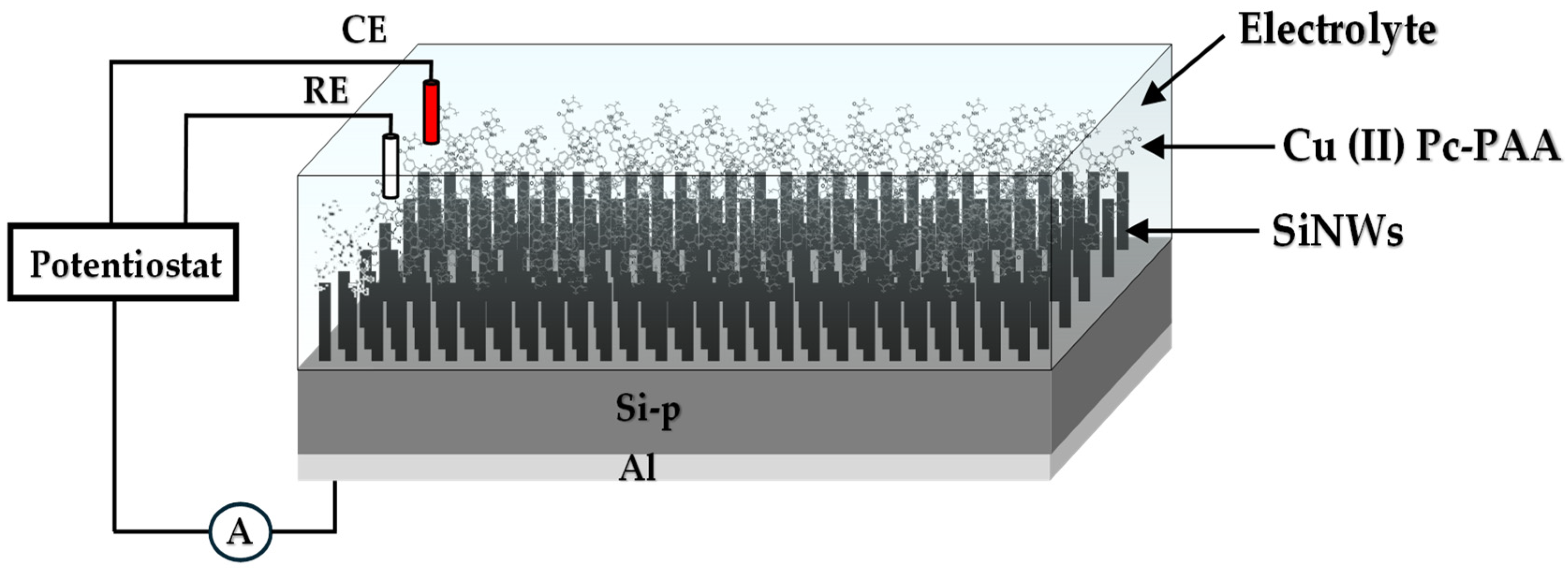
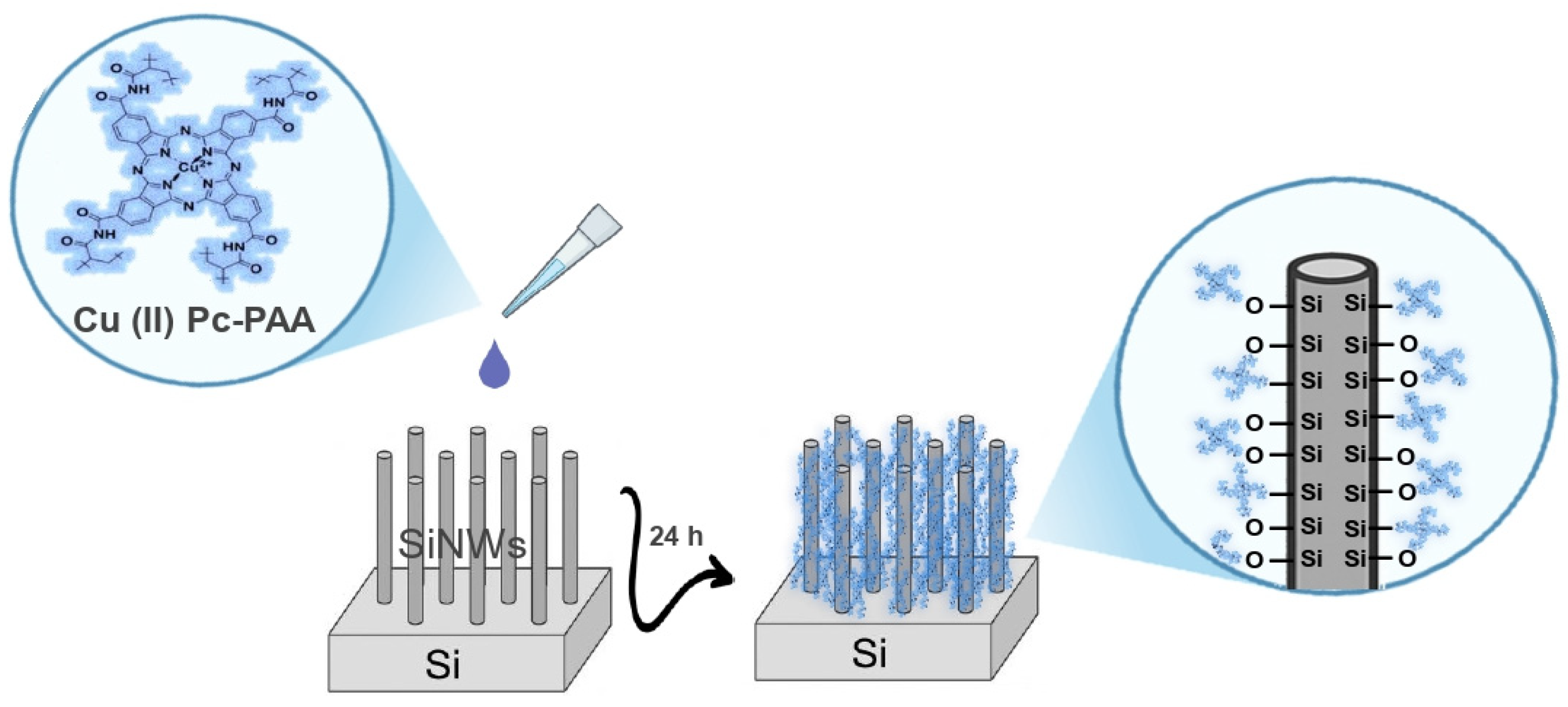
After thorough cleaning with acetone and drying under a nitrogen stream, 10 µL of the prepared Cu (II) Pc-PAA solution was drop-cast onto the electrodes surfaces and left to dry for 24 h. The Electrolyte–Insulator–Semiconductor (EIS) structure was then assembled within a custom-designed electrochemical cell, sealed with an O-ring and having a maximum volume 10 mL. Phosphate-buffered saline (PBS) was used as the electrolyte on the front side, as it provides a stable and physiologically relevant ionic environment while containing a known concentration of phosphate ions. This makes PBS an ideal model medium for assessing the sensor’s selectivity and sensitivity toward phosphate detection under controlled conditions. Moreover, since PBS is commonly employed in biological and biochemical experiments, effective phosphate detection in this medium enhances the relevance of the sensor for biomedical or clinical applications. An aluminum (Al) layer served as the ohmic contact on the back side of the device (
Figure 1). In our step, a fixed volume of 5 mL of freshly prepared PBS was used to ensure complete immersion of the electrodes and to prevent any loss of electrolyte during measurements.
The effect of Cu (II) Pc-PAA on the SiNW-based sensors was investigated using Mott–Schottky analysis. The measurements were conducted at a high frequency of 10 kHz, with the applied potential swept from −1 V to 1 V. All experiments were performed in 5 mL of freshly prepared phosphate-buffered saline (PBS, 10 mM, pH 7.2).
3. Results and Discussion
3.1. Structural Characterization
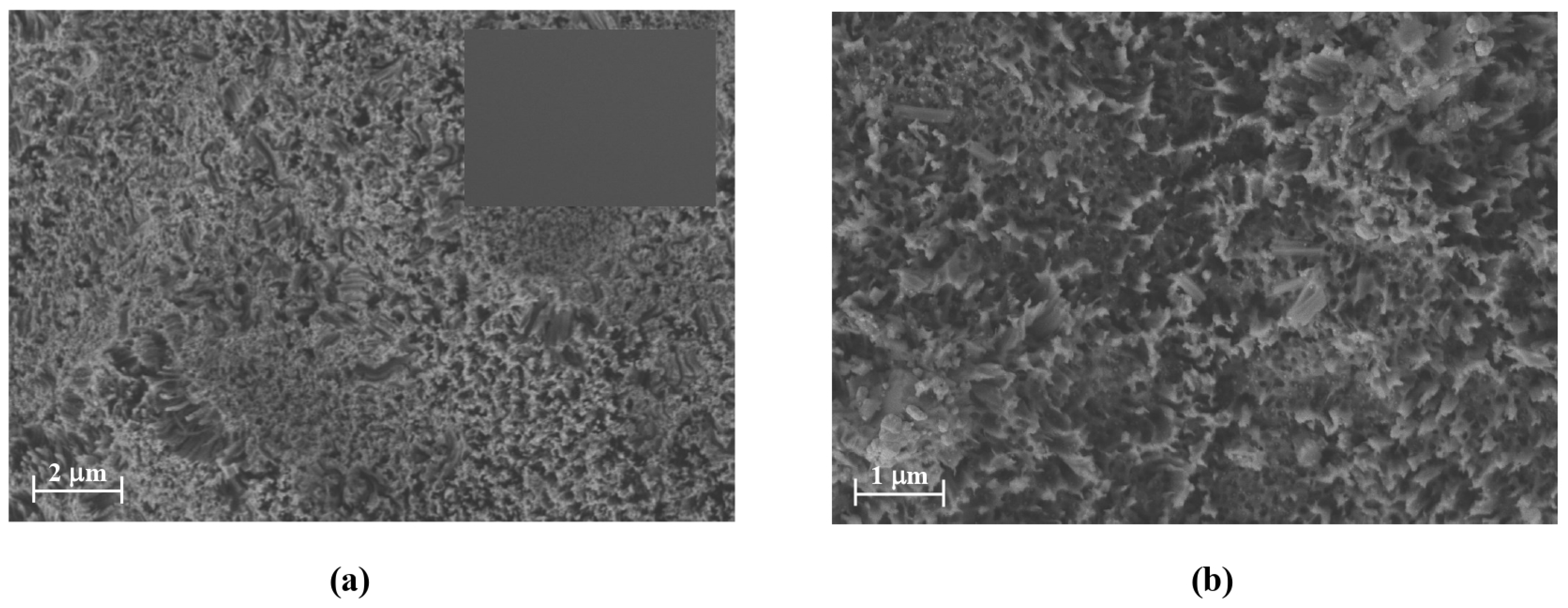
Top-view scanning electron microscopy (SEM) images of p-type silicon (Si-p) before and after a 15 min etching process are shown in
Figure 2.
The Si-p wafer initially exhibits a mirror-like surface, free from visible contamination. After etching, the formation of SiNWs is clearly observed. The top-view image (
Figure 2a) reveals a significantly rougher surface compared to the bare silicon, displaying forest-like arrays of vertically aligned SiNWs. In correlation with the size of the silver nanoparticles used, a range of pore sizes both smaller and larger was observed, randomly distributed across the surface. This irregular distribution generates a heterogeneous surface with distinct voids between individual nanowires, thereby enhancing both the porosity and the overall surface area of the material. The SiNWs exhibited diameters ranging from 7.78 to 10.66 nm, indicating moderate variability, with an overall spread of approximately 2.88 nm between the smallest and largest values. The majority of nanowires fell within the 8–10 nm range, suggesting reasonable diameter uniformity despite some heterogeneity in the growth process. These dimensional characteristics are in agreement with values reported in the literature for SiNWs synthesized under similar conditions, confirming the effectiveness and reproducibility of the applied growth method [
23].
After functionalization, the top-view SEM image (
Figure 2b) shows the SiNWs coated with the Cu (II) Pc-PAA layer, exhibiting subtle changes in surface roughness compared to the uncoated nanowires (
Figure 2a). The presence of the Cu (II) Pc-PAA layer introduced slight textural variation, resulting in a discernible alteration of the surface morphology. Additionally, the nanowires functionalized with the Cu (II) Pc-PAA membrane exhibited less distinct or slightly blurred circular tips, attributed to the conformal coating. Following surface functionalization, the average diameter of the increased from 9.05 nm to 10.87 ± 1.45 nm, confirming the successful deposition of the Cu (II) Pc-PAA layer. Furthermore, the apparent reduction in spacing between nanowire tips may result from the formation of interconnecting bridges or linkages between adjacent structures, induced by the polymeric coating. These interconnections could contribute to the less defined nanowire ends observed and are likely to enhance the structural integrity of the array, potentially improving its mechanical stability.
3.2. Optical Investigation
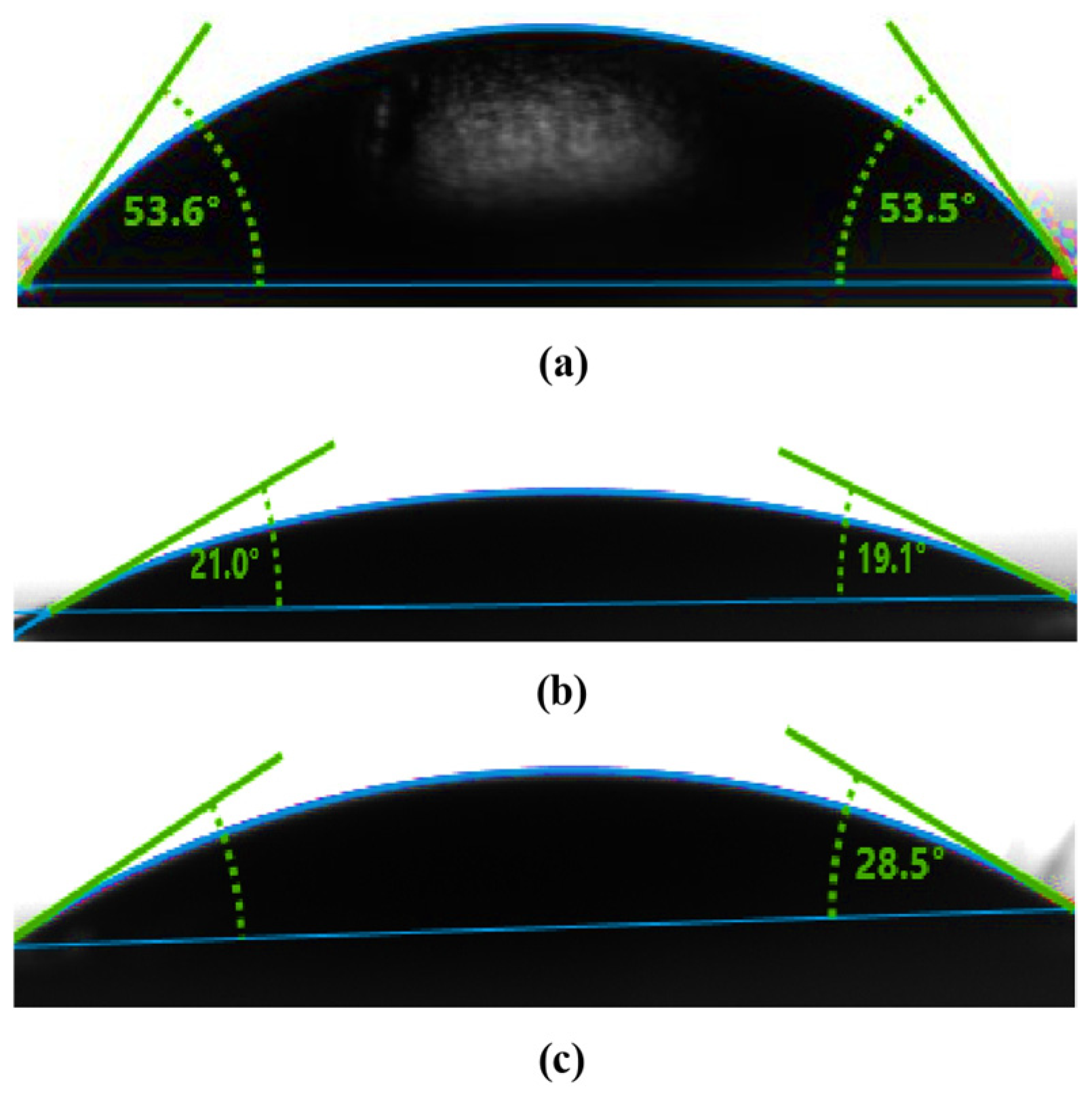
The progression of each modification step was monitored by characterizing the SiNWs before and after the functionalization using contact angle measurements (CAMs), as shown in
Figure 3.
A tangent method was employed to analyze the contact angles (CAs) of each surface, using a micrometric syringe to deposit droplets onto the substrates. High-resolution images of the droplets were then captured with a digital camera, enabling precise measurements of the contact angles. These measurements quantified the degree of hydrophobicity or hydrophilicity introduced at each modification stage, providing valuable insights into the surface energy of the nanowires. This detailed characterization was essential to understanding how each treatment influenced the SiNW surfaces and to support optimization of sensor performance for specific applications. The contact angle decreased from 53.54° to 20.03°after the etching process, indicating a significant increase in hydrophilicity (
Figure 3a,b). Consequently, the etched SiNWs exhibited enhanced water wettability, as reflected by the lower contact angle compared to bare silicon (Si).
This phenomenon can be explained by the Wenzel model, which describes how a liquid droplet on a rough surface tends to conform to the surface texture, thereby reducing the contact angle and enhancing wettability [
23]. The increased surface roughness induced by the etching process exposes a larger effective surface area, allowing water droplets to more easily penetrates the surface features.
Following functionalization of the substrate with Cu (II) Pc-PAA, the contact angle increased to 28.5° (
Figure 3c). This change is attributed to the modified surface chemistry, which decreases the material’s interaction with water [
24], rending the surface less wettable than the etched but unmodified. The observed progression in contact angle values highlights the tunability of SiNW surface properties. By controlling surface wettability, sensor performance can be enhanced through the optimization of specific interactions with targets analytes, depending on the hydrophobic or hydrophilic character of the functionalized surface.
3.3. Frequency Effect
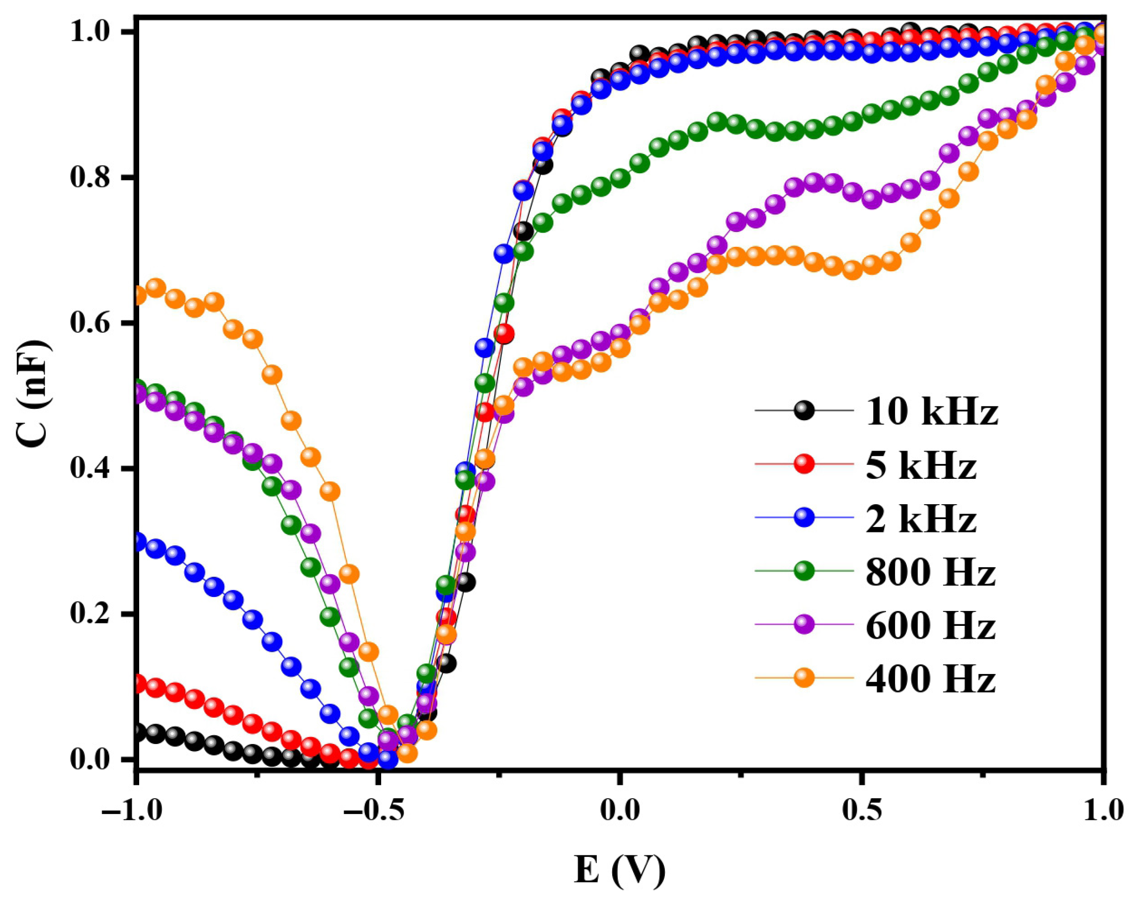
Capacitance–voltage (C-V) measurements were conducted at various frequencies ranging from 400 Hz to 10 kHz in phosphate-buffered saline (PBS, 10 mM, pH 7.2), as shown in
Figure 4.
At the lowest frequency (400 Hz), the C-V curves exhibited typical low-frequency behavior, revealing accumulation, depletion, and inversion regions, as previously reported [
24]. In the accumulation region, majority carriers (holes in p-type Si) gather at the semiconductor/oxide interface, resulting in a capacitance value close to that of the oxide layer (C
ox). In the inversion region, minority carriers (electrons in p-type Si) accumulate at the interface and can adequately respond to the slowly varying alternating current (AC) signal. This low-frequency response leads to the formation of a capacitance plateau similar to that observed in the accumulation region. The high capacitance values observed in both regions suggest that the oxide layer plays a dominant role in the system’s overall electrochemical response. This behavior is consistent with that of the Metal–Oxide–Semiconductor (MOS) structures under low-frequency AC excitation [
25]. Additionally, the C-V curves in the inversion region exhibited frequency dependence, reflecting the dynamics of mobile charge carriers under the applied potential. As a result, the space-charge and double-layer capacitances act in series, jointly determining the total measured capacitance.
At the highest frequency (10 kHz), the depletion region reaches its maximum width, and the measured capacitance is primarily governed by the oxide capacitance (Cox) in series with the depletion-layer capacitance. In this regime, the total capacitance becomes largely independent of the applied potential due to the limited temporal response of mobile minority carriers in the inversion region, which are unable to follow the high-frequency AC signal. As a result, their contribution diminishes, and the overall capacitance stabilizes near Cox. This transition from low- to high-frequency behavior marks the point at which mobile carriers exert minimal influence, and the oxide layer becomes the dominant component of the capacitive response. Such frequency-dependent characteristics provide valuable insight into the dielectric properties and carrier dynamics of the sensor structure. By selecting appropriate operating frequencies, one can enhance sensitivity and achieve more predictable sensor responses based solely on the stable characteristics of the oxide layer.
3.4. Etching Time Effect
Niklas et al. investigated the relationship between the dimension of silicon nanowires (SiNWs) and their sensitivity to surface charge variations in buffer solutions across different pH levels. Their findings showed that smaller SiNWs exhibited pronounced conductance changes in response to pH variations, while larger SiNWs demonstrated lower sensitivity. This enhanced sensitivity is attributed to the higher surface-to-volume ratio of smaller NWs, which amplifies their interactions with the surrounding environment. Therefore, reducing the width and/or height of SiNWs can further improve their sensitivity [
26].
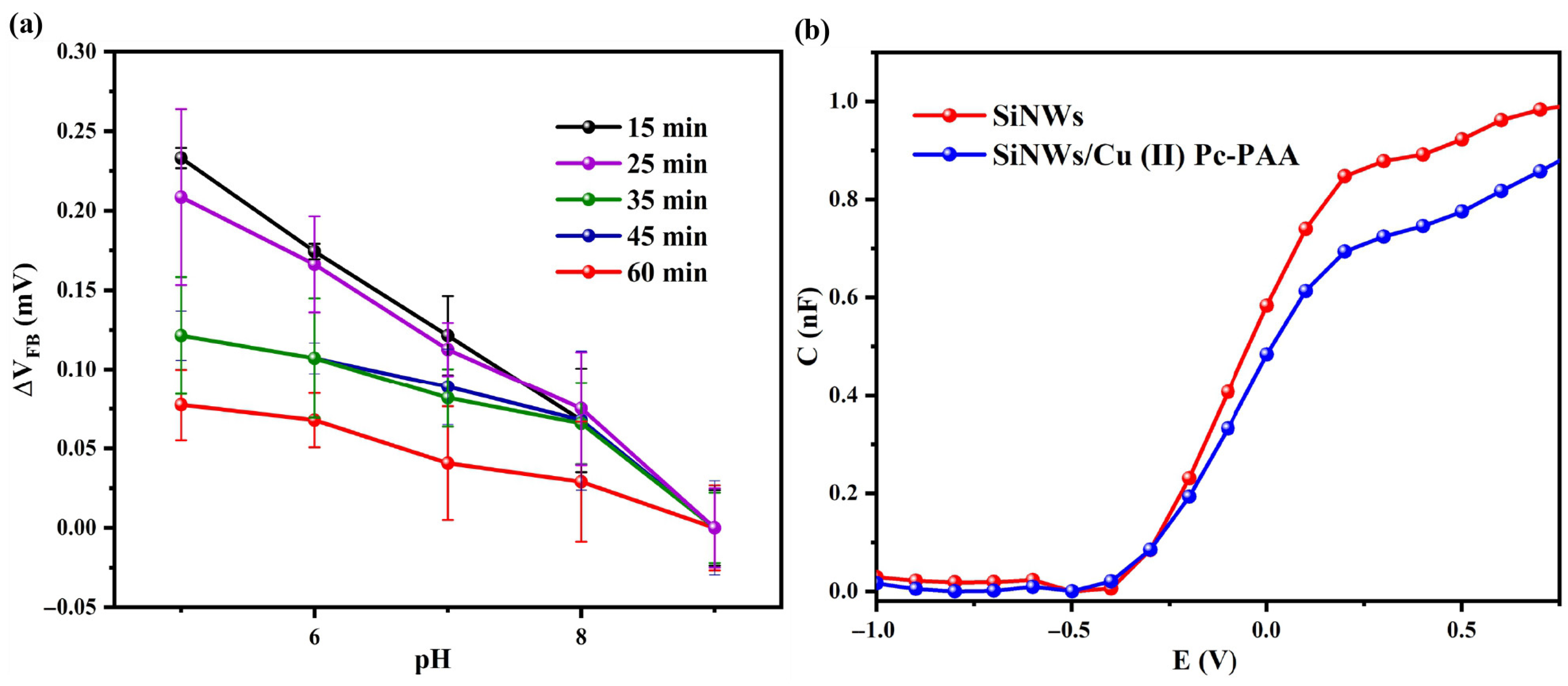
Figure 5a shows the Mott–Schottky plots of SiNWs fabricated via the MACE process with etching durations of 15, 25, 35, 45, and 60 min. The sensors were tested in 10 mM PBS solution at different pH values (5, 6, 7, 8, and 9) to evaluate their response to H
+ ions. The flat-band voltage (∆V
FB) shifted toward more positive values with increasing pH, indicating variations in surface proton concentration. The pH sensitivities were extracted from the slope of the ∆V
FB versus pH curves [
27], as summarized in
Table 1.
SiNWs fabricated with a 15 min etching duration exhibited the highest pH sensitivity, measured at 35.84 ± 0.94 mV/pH. This enhanced response is primarily attributed to an optimal surface-to-volume ratio, which increases the active surface area available for interaction with target molecules while preserving the structural integrity of the nanowires. The shorter etching duration appears to yield an ideal nanostructure morphology that facilitates efficient charge transfer and stable electrical behavior both of which are critical for reliable pH sensing. In contrast, longer etching durations (25–60 min) resulted in reduced sensitivity, likely due to over-etching, which may cause structural degradation or fusion of adjacent nanowires. Such morphological changes could decrease the effective surface area and weaken the sensor’s response to pH. Therefore, the 15 min etching duration represents an optimal compromise, maximizing accessible surface area while maintaining nanowire stability, ultimately improving overall sensor performance.
These findings underscore the critical role of the etching duration in optimizing the performance of SiNW-based pH sensors and demonstrate that precise control over fabrication parameters is essential for achieving maximum sensitivity. The results offer valuable insights into the design and development of highly sensitive electrochemical sensors based on SiNW architectures.
3.5. Mott–Schottky Analysis
Mott–Schottky (C-V) measurements of the electrochemical sensor based on SiNWs, before and after functionalization with the Cu (II) Pc-PAA sensitive layer, are shown in
Figure 5b.
In the accumulation region, the total capacitance decreased following functionalization of the transducer with Cu (II) Pc-PAA. This reduction is attributed to an increase in the effective thickness of the insulating layer [
28]. This relationship can be described by the following equation:
In Equation (1), C represents the total capacitance, is the dielectric permittivity, S is the surface = area of the working electrode, and e is the thickness of the insulating layer. The dielectric permittivity ε is defined as ε = ε0εr, where ε0 is the vacuum permittivity and εr is the relative permittivity of the insulating material.
The Cu (II) Pc-PAA is highly hydrophobic [
29], which considerably reduces the likelihood of film desorption when the electrode is immersed in an aqueous electrolyte solution. This hydrophobicity plays a crucial role in maintaining film integrity under electrochemical conditions. The Cu (II) Pc-PAA layer exhibited strong adhesion to the SiNW surfaces, primarily due to surface modifications that enhance molecular interactions and promote long-term sensor stability. This robust attachment is governed by the formation of covalent amide linkages (–CONH–) between the Cu (II) Pc-PAA molecules and functional groups on the SiNW surface, effectively preventing delamination or degradation during sensing operations [
30]. In addition to covalent bonding, the functional layer introduces specific functional groups strategically positioned on the nanowire surface, acting as active sites for selective analyte recognition and binding. Beyond covalent interactions, a dense network of non-covalent forces, including hydrogen bonding, electrostatic interactions, van der Waals forces, and π–π stacking, further reinforces interfacial adhesion. These interactions occur between the pendant groups of Cu (II) Pc-PAA structure and surface hydroxyl groups (-Si-OH), as well as directly with silicon atoms exposed on the surface of nanowire surface. Collectively, the combination of covalent and non-covalent interactions ensures stable and uniform adhesion of the functional coating to both oxidized and pristine regions of the SiNWs, thereby enhancing the overall stability and quality of the hybrid interface [
30] (
Figure 6).
Furthermore, the Cu (II) Pc-PAA layer establishes a favorable microenvironment that promotes the selective binding of phosphate ions, while effectively suppressing interference from competing species present in solutions.
This selective behavior, combined with the large surface area provided by the SiNW architecture, significantly enhances the sensor’s detection capabilities. The synergistic interaction between the sensitive Cu (II) Pc-PAA layer and the high-aspect-ratio SiNWs results in improved sensitivity, enhanced selectivity, and faster response times toward the target analyte [
30].
3.6. Sensor Performances
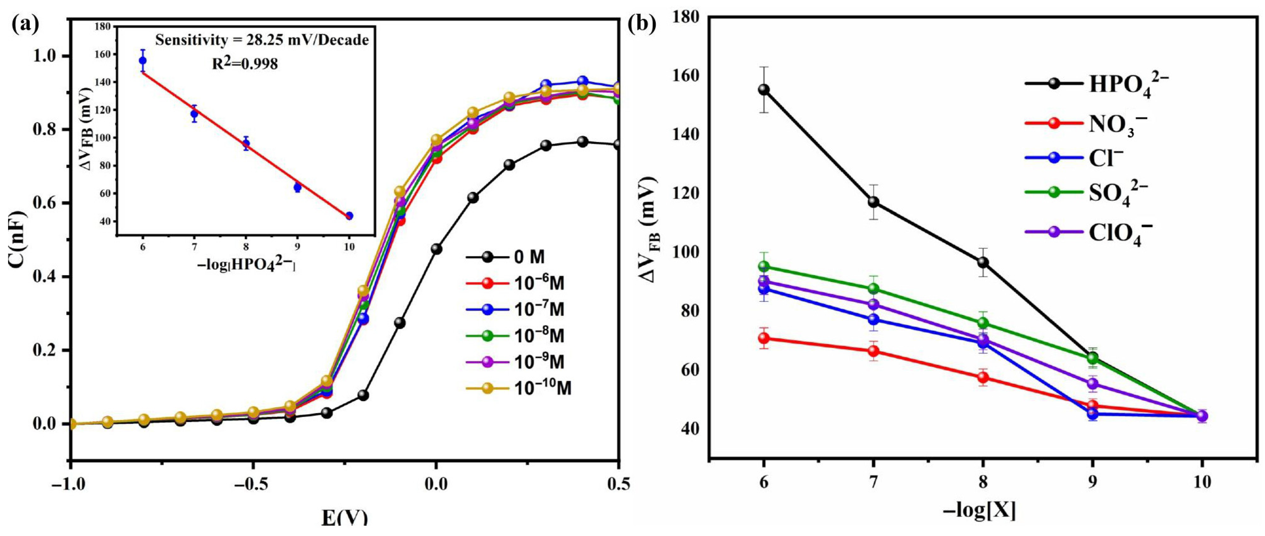
At higher frequencies, a noticeable shift in the flat-band voltage (∆VFB) was observed in the depletion region with increasing HPO
42− concentration (
Figure 7). This shift is primarily attributed to the axial coordination of HPO
42− ions to the copper (Cu) center of the phthalocyanine ring, which alters the surface potential of the Cu (II) Pc-PAA functional layer [
31]. Meanwhile, the capacitance in the accumulation region remained relatively stable, indicating that the primary sensing mechanism arises from surface potential modulation rather than changes in the bulk dielectric properties. This behavior suggests that the adsorption of charged species modifies the effective thickness of the sensitive layer, thereby influencing ∆V
FB more than the overall capacitance. To assess sensor performance, the variation in ∆V
FB was plotted as a function of HPO
42− concentration (
Figure 7a). From the linear region, the sensitivity was determined to be 28.25 mV/decade, consistent with Nernstian behavior for divalent ions. The sensor demonstrated a limit of detection (LOD) of 1.5 nM, with a detection range spanning from 10
−10 to 10
−6 M, demonstrating high effectiveness for phosphate detection at trace levels. Furthermore,
Figure 7b shows the variation in ∆V
FB as a function of −log [X] for different species, including phosphate and common interfering ions such as chloride (Cl
−), sulfate (SO
42−), nitrate (NO
3−), and perchlorate (ClO
4−). After three independent measurements, the reproducibility of our sensor was determined to be 1.53%, indicating excellent consistency and precision. The relative standard deviation (RSD) remained below 10%, confirming the good reproducibility of the sensor.
A comparison with various phosphate sensors reported in the literature highlights the diversity of interface materials and electrochemical techniques used for phosphate ion detection, along with their carrying performance characteristics. This includes screen-printed (MPP) graphene, MIP-phosphate electrodes, and laser-scribed graphene oxide, all employing differential pulse voltammetry (DPV), with limits of detection (LOD) 2.2 µM, 0.1 µM, and 0.4 µM, respectively [
6,
32,
33]. A Cobalt carbon electrode using linear sweep voltammetry (LSV) achieves an LOD of 1.43 ppm [
9], while sensor-based onCoQNRs/PBI/MWCNT/GCE and Cobalt-decorated graphene nanocomposite, using cyclic voltammetry (CV), reported LODs of 0.1 µM and an unspecified value, respectively [
34]. Notably, the Al/Si-p/SiNWs/Cu (II) Pc-PAA sensor developed in this study, using the Mott–Schottky technique, demonstrates superior performance with the lowest LOD of 0.0015 µM and a practical linear detection range from 10
−4 to 1 µM.
This remarkable sensitivity represents a significant advancement in phosphate ions detection technologies, particularly for applications requiring the measurement of extremely low concentrations. The range of linear detection reported in the literature varies from narrow intervals such as 1–20 µM (laser-scribed graphene oxide) to broader ranges like 0.1–105 µM (MIP-phosphate electrode), reflecting the diversity of operational windows tailored to specific analytical needs. These comparative findings underscore the exceptional performance of the sensor developed in this study, positioning it as a strong candidate for high sensitivity phosphate detection in complex and demanding environments.
Three electrochemical sensing interfaces for phosphate ion detection have been previously reported, each employing distinct detection mechanisms and electrode architectures, but all incorporating a copper (II) phthalocyanine derivative (Cu (II) Pc-PAA) as the active material. The Al-Cu/Si-p/ SiO
2/Si
2N
4/Cu (II) Pc-PAA interface, which utilizes impedance spectroscopy, demonstrates the widest linear detection range (0.01 to 1000 µM) and the detection limit of 0.0082 µM. In contrast, another configuration of the same structure exhibits the lowest detection limit of 0.001 µM, with a narrower linear range from 0.0001 to 0.1 µM, and achieves a sensitivity of 27.7 mV/Decade. Additionally,
Table 2 presents two interfaces employing the Mott–Schottky technique: Si-p/SiNWs/Cu (II) Pc-PAA and Al/Si-p/SiNWs/Cu (II) Pc-PAA. Both configurations exhibit identical limit of detection (0.0015 µM) and the same linear range (0.0001 to 1 µM) but differ slightly in sensitivity: 27.42 and 28.25 mV/Decade, respectively. The slight improvement suggests that the inclusion of the aluminum layer enhances the sensor’s electrochemical response. This systematic comparison highlights how subtle variations in material composition and detection techniques can influence key sensor performance metrics such as limit of detection (LOD), linear range, and sensitivity. The incorporation of SiNWs in the latter two interfaces offers a promising strategy to enhance the sensor’s surface area and detection capability. Our capacitive sensor, based on the Al/Si-p/SiNWs/Cu (II) Pc-PAA structure and employing Mott–Schottky techniques, achieves balanced performance: an LOD of 0.0015 µM, a moderate linear range (10
−4 to 1 µM) and a competitive sensitivity of 28.25 mV/Decade. Overall, the use of SiNWs enables a favorable compromise between sensitivity and operational range, making the sensor well-suited for applications requiring reliable phosphate ion detection at trace levels.
3.7. Interferences Studies
A key attribute of any electrochemical sensor is its specificity toward the target analyte. In this study, the sensor developed using the Al/Si-p/SiNWs/Cu (II) Pc-PAA structure, exhibited excellent selectivity and performance for the detection of HPO
42− ions compared to common interfering ions, such as chloride (Cl
−), sulfate (SO
42−), nitrate (NO
3−), and perchlorate (ClO
4−).
Figure 7b shows the shifts in flat-band voltage (ΔV
FB) induced by these ions, demonstrating minimal interference and highlighting the sensor’s strong and specific response to phosphate ions. The sensitivities toward NO
3−, Cl
−, SO
42−, and ClO
4− were significantly lower than that observed for HPO
42−, confirming the high specificity of the sensor for phosphate ion detection (
Table 3).
The high selectivity of the sensor can be attributed to the strong interaction between phosphate ions and the Cu (II) Pc-PAA sensing layer, which contains functional groups capable of selectively coordinating with HPO42−. This exceptional affinity leads to significantly higher sensitivity compared to other interfering species. The specificity of the sensor was rigorously evaluated against common interfering ions, including chloride (Cl−), sulfate (SO42−), nitrate (NO3−), and perchlorate (ClO4−), all of which induced minimal interference. These results confirm the strong selectivity of the developed sensor for phosphate detection. In addition to its specificity, the sensor exhibits robust stability, making it particularly suitable for real-world environmental applications, such as monitoring phosphate levels in natural water bodies (rivers, lakes, seas), where interference is often a major challenge.
Given its high sensitivity, low detection limit, and excellent selectivity, the proposed sensor is well-positioned for integration into portable, in situ environmental monitoring systems. Its reliable and repeatable performance in complex aqueous environments highlights its potential to support initiatives in water quality assessment, eutrophication control, and aquatic ecosystem protection.
4. Conclusions
In this study, we developed a high-performance electrochemical sensor based on silicon nanowires (SiNWs), functionalized with a novel copper (II) phthalocyanine derivative (Cu (II) Pc-PAA) as the sensing layer, for the selective detection of phosphate ions. The sensor exhibited outstanding performance across diverse operational conditions, with capacitance measurements performed at both low and high frequencies, offering valuable insights into its electrochemical behavior and dynamic response under varied environments.
Phosphate ions were reliably detected over a wide concentration range (10−10 to 10−6 M), achieving an impressive limit of detection (LOD) of 1.5 nM. The advanced analytical capability is attributed to the synergistic effects of the high surface area provided by the SiNWs architecture and the strong affinity of the Cu (II) Pc-PAA layer for phosphate ions. The resulting structure enabled enhanced interfacial interactions, high Nernstian sensitivity, and excellent measurement repeatability. Importantly, the sensor demonstrated strong selectivity against common interfering ions such as chloride (Cl−), sulfate (SO42−), nitrate (NO3−), and perchlorate (ClO4−), with minimal signal deviation. This high selectivity combined with its structural stability, positions the Al/Si-p/SiNWs/Cu (II) Pc-PAA sensor as a robust platform for real-world environmental applications. Altogether, these results confirm the strong potential of the proposed sensor for accurate, reliable, and in situ monitoring of phosphate levels in complex aqueous media, including rivers, lakes, and marine environments, where selective and sensitive detection remains a critical challenge for water quality management and environmental protection.
The exceptional sensitivity, selectivity, and low detection limit achieved by the developed sensor offer strong potential for broader environmental applications. Its ability to deliver reliable, repeatable measurements in complex aqueous environments makes it a valuable tool for environmental monitoring and pollution control, supporting efforts to protect aquatic ecosystems. Future optimizations could enable its integration into portable, autonomous, and in situ phosphate monitoring devices, critical for addressing environmental challenges such as eutrophication and ensuring effective water quality management. To further enhance its practical applicability, future research should focus on evaluating the sensor’s long-term stability, reproducibility across multiple fabrication batches, and real-time detection capabilities. Additionally, assessing its performance under varying environmental conditions, such as changes temperature, pH, and ionic strength, will be essential for robust deployment in diverse and dynamic aquatic systems. These efforts will pave the way for the development of a fully optimized sensor suitable for both natural and industrial water quality monitoring.
