Article

Enhanced NO2 Detection in ZnO-Based FET Sensor: Charge Carrier Confinement in a Quantum Well for Superior Sensitivity and Selectivity

1
Sensor Lab, Department of Information Engineering, University of Brescia, Via Valotti 9, 25133 Brescia, Italy
2
Laboratoire de Micro-électronique Appliquée, Université Djillali Liabès de Sidi Bel Abbès, Sidi Bel Abbès 22000, Algeria
*
Author to whom correspondence should be addressed.
Chemosensors 2025, 13(10), 358; https://doi.org/10.3390/chemosensors13100358
Submission received: 9 August 2025 / Revised: 22 September 2025 / Accepted: 29 September 2025 / Published: 1 October 2025
(This article belongs to the Special Issue Functionalized Material-Based Gas Sensing)

Abstract

NO2 is a toxic gas mainly generated by combustion processes, such as vehicle emissions and industrial activities. It is a key contributor to smog, acid rain, ground-level ozone, and particulate matter, all of which pose serious risks to human health and the environment. Conventional resistive gas sensors, typically based on metal oxide semiconductors, detect NO2 by resistance modulation through surface interactions with the gas. However, they often suffer from low responsiveness and poor selectivity. This study investigates NO2 detection using nanoporous zinc oxide thin films integrated into a resistor structure and floating-gate field-effect transistor (FGFET). Both Silvaco-Atlas simulations and experimental fabrication were employed to evaluate sensor behavior under NO2 exposure. The results show that FGFET provides higher sensitivity, faster response times, and improved selectivity compared to resistor-based devices. In particular, FGFET achieves a detection limit as low as 89 ppb, with optimal performance around 400 °C, and maintains stability under varying humidity levels. The enhanced performance arises from quantum well effects at the floating-gate Schottky contact, combined with NO2 adsorption on the ZnO surface. These interactions extend the depletion region and confine charge carriers, amplifying conductivity modulation in the channel. Overall, the findings demonstrate that FGFET is a promising platform for NO2 sensors, with strong potential for environmental monitoring and industrial safety applications.

1. Introduction

Gas sensors are increasingly important across fields such as environmental safety and healthcare. Metal–oxide (MOX) semiconductors are widely studied because they combine high sensitivity and rapid response with [1,2,3]. Most MOX sensors are implemented in resistor-type designs, valued for their straightforward structure and fabrication. However, the two-terminal configuration restricts their ability to adjust or optimize dynamic behaviors such as response and recovery.
Beyond their use in conventional resistor-type devices, recent research highlights the advantages of integrating MOX into transistor architectures for enhanced gas detection [4]. In particular, field-effect transistor (FET) platforms provide superior control over charge transport and enable modulation of sensing characteristics through biasing schemes or gate engineering. This allows for greater sensitivity, selectivity, and stability compared to traditional two-terminal chemiresistors. Several studies have demonstrated that incorporating MOX such as In2O3, WO3, or ZnO into FET designs leads to significantly improved sensing performance toward toxic gases including NO2, NH3, and O3. For example, Andringa et al. [5] reported a ZnO FET capable of detecting NO2 down to tens of parts per billion at 200 °C, attributing the response to charge trapping at the dielectric interface. Similarly, Shin et al. [6] showed that WO3 FETs with floating-gate configurations can exploit charge storage engineering to achieve large improvements in sensitivity and recovery dynamics compared to resistor-type sensors. Their work compares WO3 chemiresistor and FET gas sensors fabricated on the same wafer. The chemiresistor shows almost constant response across applied voltages, with sensitivity increasing slightly with NO2 concentration before reaching saturation. Unlike the chemiresistor, the FET device provides greater flexibility because its multi-terminal design allows the use of biasing strategies to adjust performance. By applying charge storage engineering, the FET achieves a much stronger response and higher sensitivity than the resistor device, demonstrating the clear advantage of transistor-based architectures for gas sensing. Recently, Shin et al. [4] developed a FET-type gas sensor by integrating co-sputtered zinc indium tin oxide (ZITO) as the active channel layer. The FET configuration allowed precise modulation of charge transport and facilitated a clear link between surface chemistry and electrical transduction. By varying the ZnO/ITO ratio, they tuned the channel properties, demonstrating that oxygen-vacancy-rich films enhanced NO2 response at higher operating temperature, while hydroxyl-rich films were more effective at lower temperature. The transistor design was crucial for extracting these differences, as the gate control amplified the sensitivity and provided stability compared to conventional chemiresistors. Their results highlight how material optimization combined with a FET platform can significantly improve detection performance and adaptability of metal-oxide gas sensors.
Recent studies have shown that the morphology of ZnO is a key factor influencing its gas-sensing properties [7,8].
ZnO nanostructures exhibit diverse forms, each tailored for specific gas sensing applications. Among them, the nanoporous variant stands out due to its enhanced surface area and abundance of active sites for gas adsorption. This structure allows for gas diffusion and increases the density of interaction sites, significantly boosting the sensor’s sensitivity and responsiveness to target gases. The large surface area of nanoporous ZnO facilitates more effective adsorption and desorption of gas molecules, thereby enhancing the sensor’s ability to detect low concentrations. Its nanoscale porosity also contributes to improved catalytic activity and faster response time, making this material well-suited for high-performance gas sensing applications. Y. Nagarjuna et al. [9] have fabricated such a nanoporous structure for a highly efficient ozone gas sensor using a high-power impulse magnetron sputtering process. The sensor demonstrated optimal performance at 200 °C, with a 638% response at 1 ppm O3, but showed reduced sensitivity as relative humidity increased. They explained this sensing mechanism of the nanoporous ZnO by the adsorption and desorption processes occurring on the material surface. In another study, D. Pleshek et al. [10] have developed highly porous ZnO films using a swelling-assisted sequential infiltration synthesis method based on block copolymer templates. The resulting coatings, with thicknesses ranging from 140 to 420 nm, exhibited up to 98% pore accessibility and presented improved ethanol sensing performance, highlighting their potential for low-temperature sensing applications.
Han et al. [11] developed NH3 sensors based on organic field-effect transistors (OFETs) using poly (methyl methacrylate) (PMMA) blended with ZnO nanoparticles as the gate dielectric layer. The ZnO/PMMA hybrid dielectric significantly enhanced sensing performance, showing nearly a tenfold increase in response compared to pure PMMA at 75 ppm NH3, along with notable shifts in threshold voltage and changes in field-effect mobility. Analysis revealed that the improved sensing was due to the ZnO/PMMA hybrid layer facilitating better interaction between NH3 and the conducting channel, with the sensors maintaining stability over 40 days in ambient conditions.
Incorporating nanoporous ZnO into various electronic structures and designs significantly enhances its sensitivity in gas-sensing applications. By integrating this nanostructured material into conductometric sensors, Schottky diodes, or field-effect transistors (FETs), the unique surface characteristics of the oxide can be fully exploited.
Such designs enhance catalytic activity and accelerate charge transfer processes resulting in improved selectivity, stability, and response time, making ZnO-based nanosensors more effective in detecting low concentrations of gases in real-time applications.
In this paper, we present the simulation and fabrication of nanoporous ZnO thin-film gas sensors, based on both conventional resistor and Floating Gate Field Effect Transistor (FGFET) structures. This study specifically examines the electron confinement effect within the transistor during the detection of NO2, aiming to demonstrate its advantages over traditional resistive sensors in terms of sensitivity, response time, and overall performance. Leveraging the gas-sensing properties of ZnO and the advanced functionality of FGFETs, we explore the interaction between NO2 and the nanoporous oxide surface. To achieve this, we employed Silvaco-Atlas software (Version 3.8.46.R) to simulate the electrical behavior, energy band profiles, and potential diagrams of both sensor types under NO2 exposure. In the next phase, we plan to experimentally validate the simulation results through the fabrication and testing of the two sensor prototypes.

2. Theoretical Details

2.1. Working Principle of ZnO Sensor

The gas sensing mechanism of ZnO toward NO2 relies on surface reactions that modify its electrical properties, enabling effective detection.
Initially, when ZnO is exposed to air, oxygen molecules adsorb onto the surface. Depending on the temperature and surface conditions, these adsorbed oxygen are ionized into various ionic species such as O 2 , O , and O 2 by the following equations [12].
O 2 ( g a s )   O 2 ( a d s )
O 2 a d s + e O 2 ( a d s )
O 2 a d s + e 2 O
O + e O 2
Typically, oxygen molecule ions are the dominant species at temperatures up to approximately 150 °C [13]. O species prevail between 150–300 °C [14], forming a single electropositive oxygen vacancy V O + [15] and O 2 species become dominant at temperatures above 300 °C [16] creating a double electropositive oxygen vacancy V O + + [15] as illustrated in Figure 1 [17]. This process of the extraction of electrons from the surface of the porous ZnO results in the formation of an electron depletion layer near the surface.
When NO2 gas is introduced, it can either directly adsorb onto the surface of the gas sensor or react with the pre-adsorbed oxygen species [18,19,20], as described by the following reactions:
N O 2 + e   N O 2
N O 2 + O   N O 2 + 1 2 O 2
N O 2 + O   2 O 2 + N O 2
These reactions further reduce the electron concentration at the ZnO surface, causing the depletion region to extend deeper into the material and increasing the resistance of the sensor, as the conductive path for the electron current becomes narrower.

2.2. Modeling Gas Diffusion and Surface Kinetics in Porous ZnO

The overall sensor response is affected by both surface reaction and gas diffusion rates. The rate of gas diffusion is determined by the microstructure of the sensing layer, the size of the target gas molecules, and Knudsen diffusion.
The Knudsen diffusion coefficient is expressed as [21,22]:
D k =   4 r 3 2 R T π M 1 2
where:
T: temperature.
r: pore radius.
M: molecular mass of the gas molecules.
R  = 8.314 J.mol−1.K−1: gas constant.
Sakai et al. [23] modeled the gas concentration in relation to the sensing porous film thickness deposited on a substrate using the following diffusion-reaction equation:
C A t = D k 2 C A x 2 k C A
where:
C A : concentration of the diffusing/reacting gas.
t: time.
x: spatial coordinate (along diffusion direction).
k : surface reaction rate.
D k : diffusion coefficient.
The equation applies considering that the diffusion follows the Knudsen mechanism. The gas concentration profile is derived by solving the equation assuming steady-state conditions (∂ C A /∂t = 0), which depends on the film thickness, surface reaction rate, and diffusion coefficient, obtaining the following equation.
C A = C A , S c o s h ( L x × m ) c o s h ( L × m )  
where:
C A , S : concentration of the gas at the surface.
L: film thickness.
m = k D k : the reaction-diffusion parameter that represents how strongly the reaction rate dominates over diffusion (it is also defined as the inverse characteristic diffusion length).
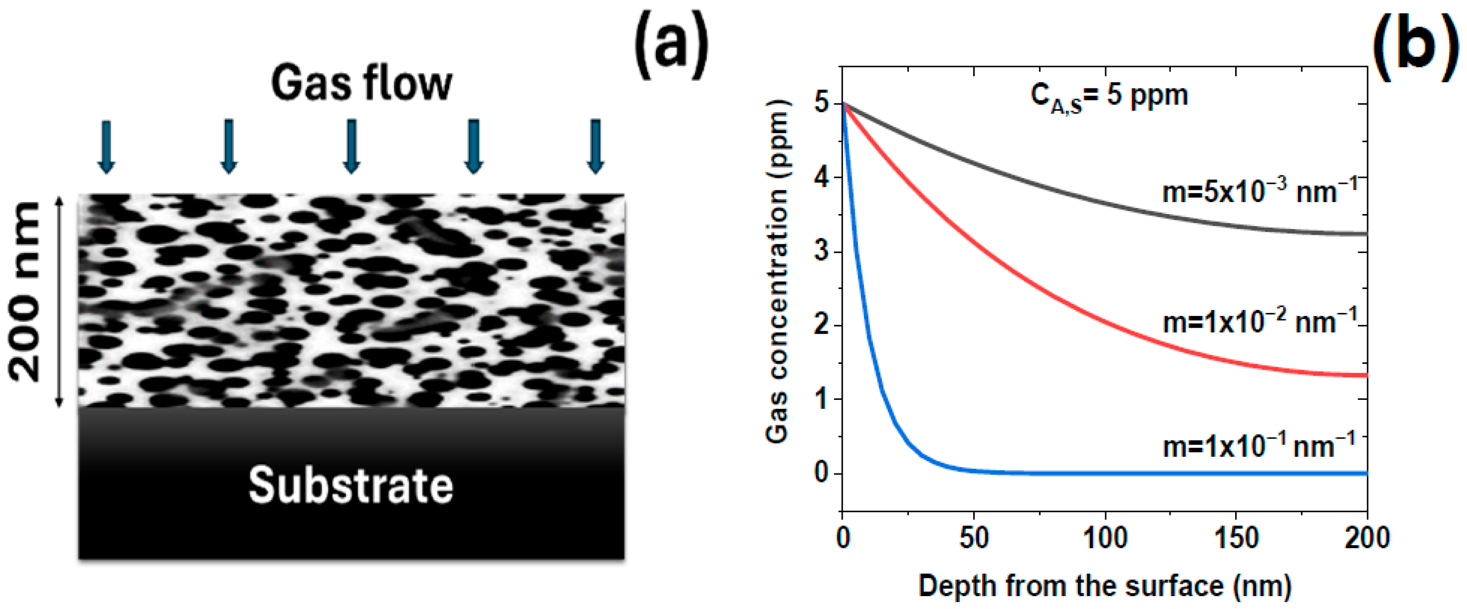
Using Sakai et al. model, a simulation of gas concentration within a porous film of 200 nm-thickness deposited on a substrate (Figure 2a) was performed for gas flow of 5 ppm, at different m values (Figure 2b). As can be seen in Figure 2b, the gas concentrations decrease exponentially with the depth from the surface. This decrease accelerates at higher m values indicating that most reactions between the gas and the sensing layer occur close to the surface.
Based on the above results, Silvaco-Atlas software was used to simulate FGFET and conventional resistor gas sensors incorporating a 200 nm ZnO thin film, by taking into consideration the gas behavior of m = 1 × 10 2 n m 1 . This value of m was estimated as an intermediate representative parameter, chosen to avoid bias toward either slow or fast diffusion limits. This parameter serves as an illustrative example to study the effect of charge-carrier confinement in a quantum well. It is not intended to represent an exact physical value but rather to emphasize the confinement effects. Silvaco-Atlas is a versatile tool for simulating and analyzing semiconductor devices and integrated circuits. It provides a comprehensive framework for modeling diverse devices using fundamental equations, including Poisson’s equation and the continuity equations for electron and hole transport.
The Poisson equation, which describes the relationship between the electrostatic potential and the spatial charge density, is expressed as:
d i v ε ψ = ρ
where ψ represents the electrostatic potential, ε denotes the permittivity, and ρ is the space charge density.
The continuity equations for electron and hole carriers are given by [24]:
n t = 1 q d i v   j n + g n r n  
p t = 1 q d i v   j p + g p r p  
where n and p are the electron and hole concentrations, j n and j p are the electron and hole current densities, g n and g p are the generation rates for electrons and holes, r n and r p are the recombination rates for electrons and holes, and q is the elementary electric charge.
Equations (11)–(13) provide the general framework for device simulation. However, Silvaco-Atlas also includes additional secondary equations to describe specific physical models for parameters like g n , r n , g p , and r p . The current density equations, or charge transport models, are typically obtained by applying approximations and simplifications to the Boltzmann transport equation. Depending on the assumptions, different transport models can be derived, including the drift-diffusion, energy balance transport, and hydrodynamic models [25].
Several physical models are implemented in the simulations. These include the Shockley–Read–Hall (SRH) recombination and Auger recombination rate models to account for trap-assisted tunneling and the minority recombination effects, Lombardi CVT model for electric field-, temperature-, and concentration-dependent mobility calculations, Fermi Dirac statistics for carrier distribution, FLDMOB to describe mobility under lateral electric field, and CONSRH (a defect-free SRH recombination model) for bandgaps.
Additionally, the effect of NO2 gas is incorporated by introducing the density of states (DOS) within the bandgap that act as electron acceptors. These states capture electrons from the conduction band, thereby altering the sensor’s electronic properties [26,27,28], as illustrated in Figure 1.
The DOS is composed of four bands: two tail bands (a donor-like valence band g T D ( E ) and an acceptor-like conduction band g T A ( E ) ), modeled using an exponential distribution, and two deep-level bands (one donor-like g G D ( E ) and one acceptor-like g G A ( E ) ), modeled using a Gaussian distribution. This can be expressed as follows [25]:
g T A E =   N T A   e x p E E c ω T A
g T D E = N T D   e x p E v E ω T D
g G A E = N G A   e x p E G A E ω G A 2
g G D E = N G D   e x p E E G D ω G D 2
where E represents the trap energy, E c denotes the conduction band energy, E v refers to the valence band energy, and ω symbolizes the characteristic decay energy. The subscripts T, G, A, and D correspond to tail states, Gaussian (deep level) states, acceptor states, and donor states, respectively.
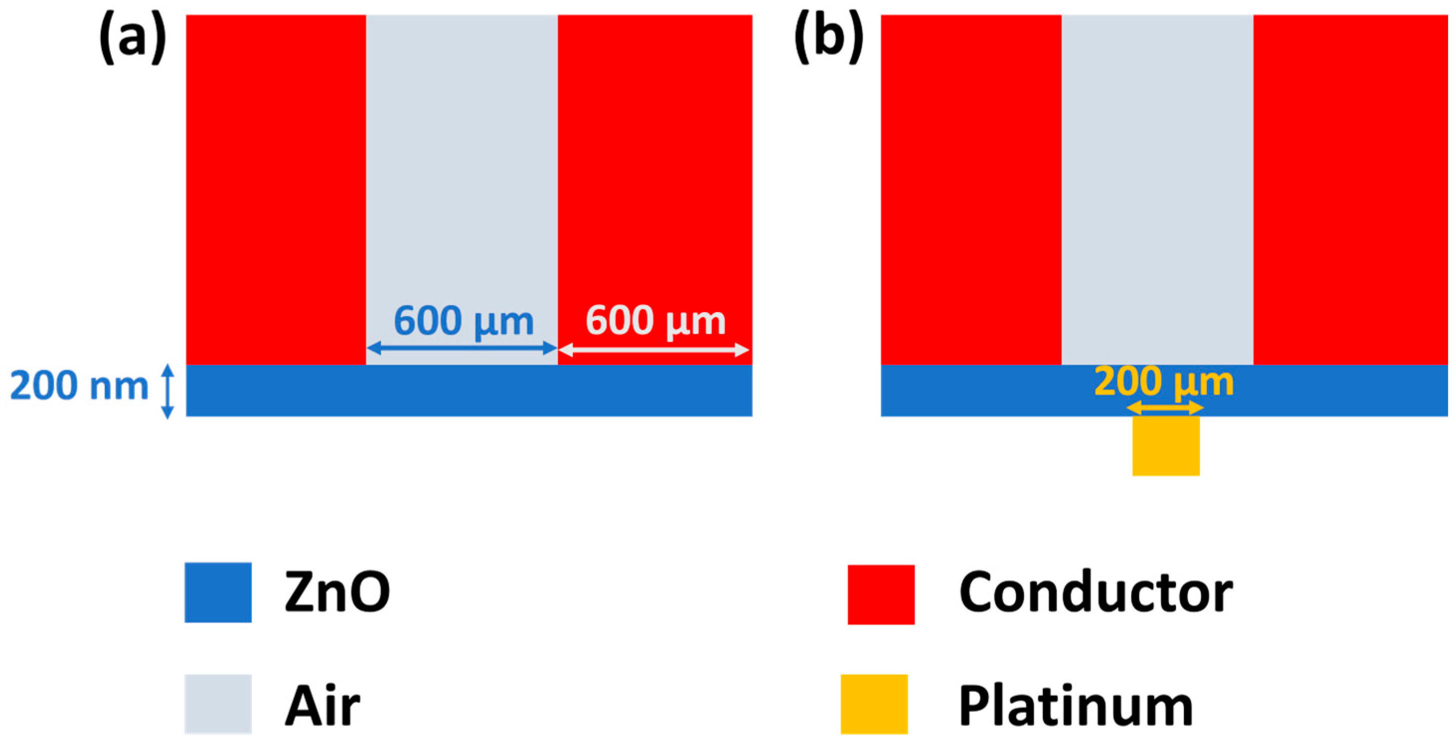
Figure 3a,b show the device architectures of the conventional resistive gas sensor and the FGFET-based gas sensor, respectively. Both configurations use a 200 nm-thick n-type ZnO sensing layer, with an intrinsic charge carrier concentration of 5 × 1017 cm−3. The two sensor structures share a common layout featuring a pair of top-deposited ohmic contacts, each 1 µm thick and 600 nm wide, spaced 600 nm apart on the ZnO surface.
In the FGFET design, a Schottky gate electrode made of platinum (Pt) is integrated beneath the ZnO layer. This gate is 100 nm thick and 200 µm wide. Additionally, an air gap is defined above the ZnO film, between the two ohmic contacts, to simulate the gas exposure environment.
During the simulation, Silvaco-Atlas assigns relevant physical and electrical properties to each material involved, including parameters such as bandgap energy, electron affinity, dielectric permittivity, and carrier mobility. These material-specific parameters are crucial for accurately modeling the electrical response and overall performance of the gas sensing devices.

3. Experimental Details

3.1. Fabrication Process

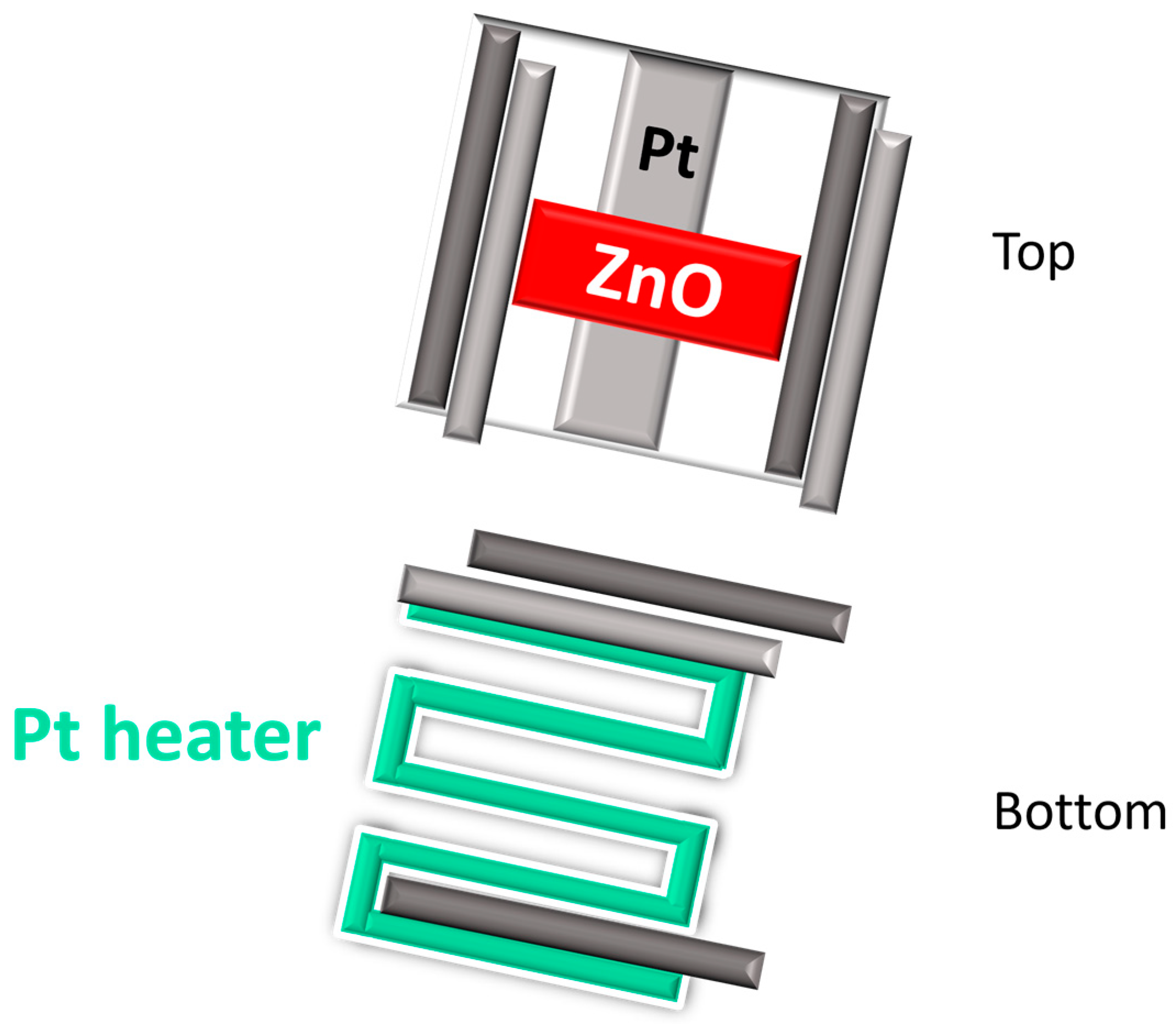
The FGFET and resistive gas sensor structures were fabricated following the simulation designs. Alumina (Al2O3) substrates (2 mm × 2 mm, 2N purity, Kyocera, Japan) were first cleaned ultrasonically in acetone for 20 min, rinsed with ethanol, and dried in synthetic air. For the FGFET structure, a 100 nm-thick Pt layer was deposited on the alumina substrate as a gate Schottky contact using DC magnetron sputtering. A 200 nm-thick Zn layer was then deposited on both sensor structures using the same method. The samples are oxidized at 500 °C for 1 h under a partial vacuum of 0.7 mbar, with a gas flow of 20 sccm O2 and 80 sccm Ar, resulting in the formation of nanoporous ZnO material. To form the ohmic electrodes, a 50 nm TiW layer followed by 1 µm of Pt was deposited using DC magnetron sputtering at 300 °C, ensuring strong adhesion to the alumina substrates. The TiW layer provided excellent ohmic contact while enhancing adhesion. On the backside of the samples, a 50 nm TiW adhesion layer is deposited, followed by a 1.5 µm-thick Pt heating element, also using DC magnetron sputtering (see Figure 4).
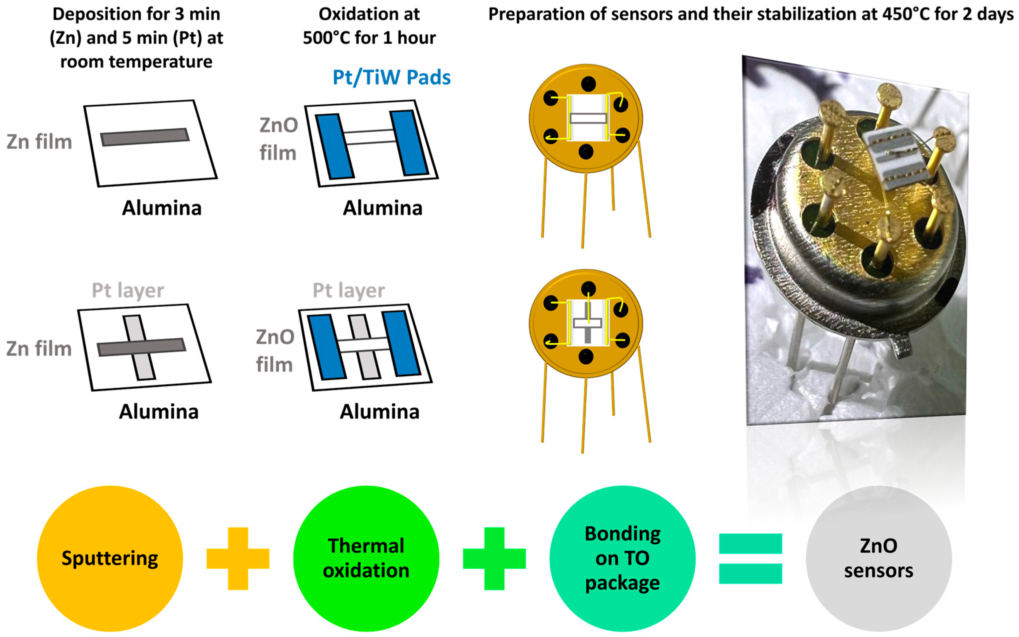
The samples were wire-bonded onto transistor outline (TO) packages using gold wires to form the sensing devices, labeled as ‘R’ for the resistor sensor and ‘TR’ for the FGFET sensor. The sensors were stabilized by aging at 450 °C for 48 h. Figure 5 illustrates the main steps in the fabrication process, from the deposition of the metallic layer to the sensors’ final readiness for gas testing.

3.2. Characterizations

The morphology of the ZnO sensing layers was characterized using a scanning electron microscope (SEM) with high-resolution (MIRA3 FEG-SEM, TESCAN). The images were captured at 7 kV, with a working distance of 10 mm and magnification of 10,000×.
To assess the gas-sensing performance of the fabricated FGFET and resistive ZnO-based sensors, functional tests were performed inside a stainless-steel climatic chamber (Angelantoni, Massa Martana, Italy, model MTC 120) with a volume of 1 L. This system accommodates up to eight sensors simultaneously, enabling parallel electrical characterization under controlled environmental conditions.
The sensor was mounted on a 6-pin transistor outline (TO) package as shown in Figure 5, although only four pins were used during the measurements:
  • Two pins were connected to the platinum heater on the backside of the alumina substrate, ensuring precise thermal control of the device;
  • The remaining two pins were connected to the Pt pads on the top ZnO surface for electrical signal measurement.
The TO packages were arranged in the climatic chamber in a consistent configuration, allowing for simultaneous application of heating and real-time conductance monitoring of the active sensing layer.
The target gas concentrations were prepared by diluting certified standard gases (SOL, Italy) with synthetic air using mass flow controllers to obtain the desired levels. The total gas flow was maintained at 200 standard cubic centimeters per minute (sccm) throughout all tests. Each measurement cycle included:
  • 30 min of exposure to the target analyte,
  • followed by 90 min of synthetic air flow to allow the sensor to return to its baseline conductance.
The electrical response of the sensors was measured by applying a constant voltage ranging from 1 V to 10 V (1 V in our measurement) using an Agilent E3631A DC power supply. The resulting current was continuously monitored using a Keithley 6485 picoammeter, enabling real-time calculation of conductance values.
Sensors were tested toward various oxidizing (e.g., NO2) and reducing gases (e.g., NH3, H2, ethanol) to evaluate selectivity, sensitivity, and repeatability. The relative humidity (RH) inside the chamber was controlled and varied between 0% (dry air) and 80%, to investigate the effect of moisture on sensor response.
All measurements were performed at controlled working temperatures ranging from 150 °C to 400 °C, adjusted using Thurlby Thandar PL330DP power supplies, while the ambient chamber temperature was kept constant at 20 °C. Sensors were preconditioned by thermal aging at 450 °C for 48 h before testing to ensure signal stability and repeatability.
The response ( Δ G G ) of each sensor was calculated using the following expressions:
Upon the introduction of the oxidizing (reducing) gas, the response of the devices is calculated as Δ G G = G a i r G g a s G g a s   ( Δ G G = G g a s G a i r G a i r ).

4. Results and Discussions

4.1. Modelling Results

The simulated current–voltage (I–V) characteristics of the fabricated sensor architectures were obtained using Silvaco-Atlas to assess and compare their electrical responses in the presence and absence of NO2.
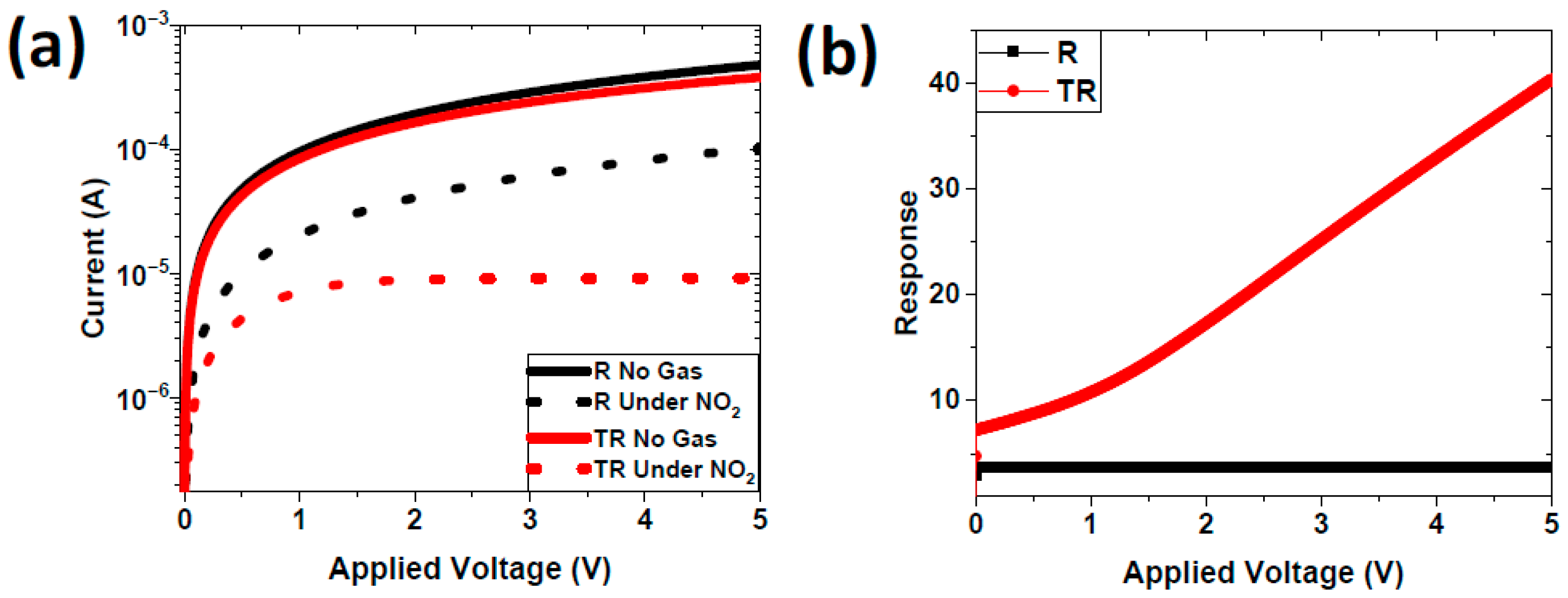
Figure 6a shows the I–V curves extracted from the ohmic contacts of the resistor and FGFET gas sensors, noted R and TR, respectively, with and without the presence of NO2 gas, at 300 °C.
Both structures display comparable I–V characteristics, with minor deviations at higher voltages likely caused by the gate effect. The current in both cases rises exponentially with increasing applied voltage. Upon exposure to NO2, both structures show a decrease in the current, with a larger reduction for the FGFET. This occurs because, when the applied voltage exceeds 1.5 V, the current of the FGFET remains nearly constant at approximately 8.85 × 10⁻⁶ A, making the reduction more pronounced at higher voltages, unlike the resistor, which exhibits a steady decrease with increasing the applied voltage.
These results demonstrate that the FGFET structure is substantially more sensitive to NO2 than the resistor sensor. This is further illustrated in Figure 6b, showing the response versus applied voltage calculated as follows,
R e s p o n s e = ( I N o   g a s I U n d e r   g a s ) / I U n d e r   g a s
The FGFET demonstrates a substantially stronger response to NO2 than the resistor sensor, and its sensitivity increases with applied voltage, unlike the resistor, which maintains a nearly constant response. The enhanced performance of the FGFET is attributed to its floating gate, which amplifies variations in surface charge induced by NO2 adsorption on the ZnO layer.
To gain further insight into these effects, the influence of NO2 on the energy band structure and potential distribution for both sensor configurations is examined in the following section.
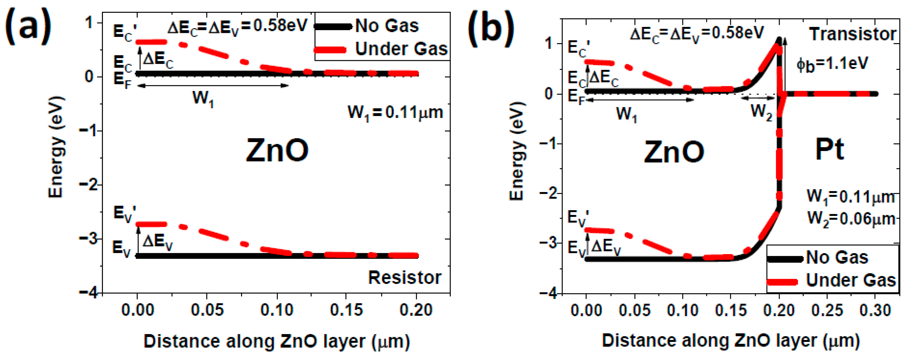
Figure 7a,b display the energy band diagram for the resistor and FGFET gas sensors, respectively, highlighting the impact of NO2 on their energy profiles. At the ZnO/Pt interface, a Schottky barrier with a height of ɸ b = 1.1   e V and a depletion region with a width of W 2 = 60   n m are established. Upon introducing NO2, significant band bending occurs in both devices as the gas molecules withdraw electrons from the ZnO surface, forming an electron depletion region with a width of W 1 = 110   n m . This induces a shift in the conduction and valence band edges (Ec and Ev) by 0.58 eV, resulting in more pronounced bending near the surface.
Furthermore, in the FGFET, the combined effect of the Schottky barrier and band bending generates a quantum well in the conduction channel, which confines charge carriers and amplifies the sensor’s response. This quantum well effect enhances the modulation of channel conductivity, rendering the FGFET significantly more sensitive to NO2 than the resistor-type sensor.
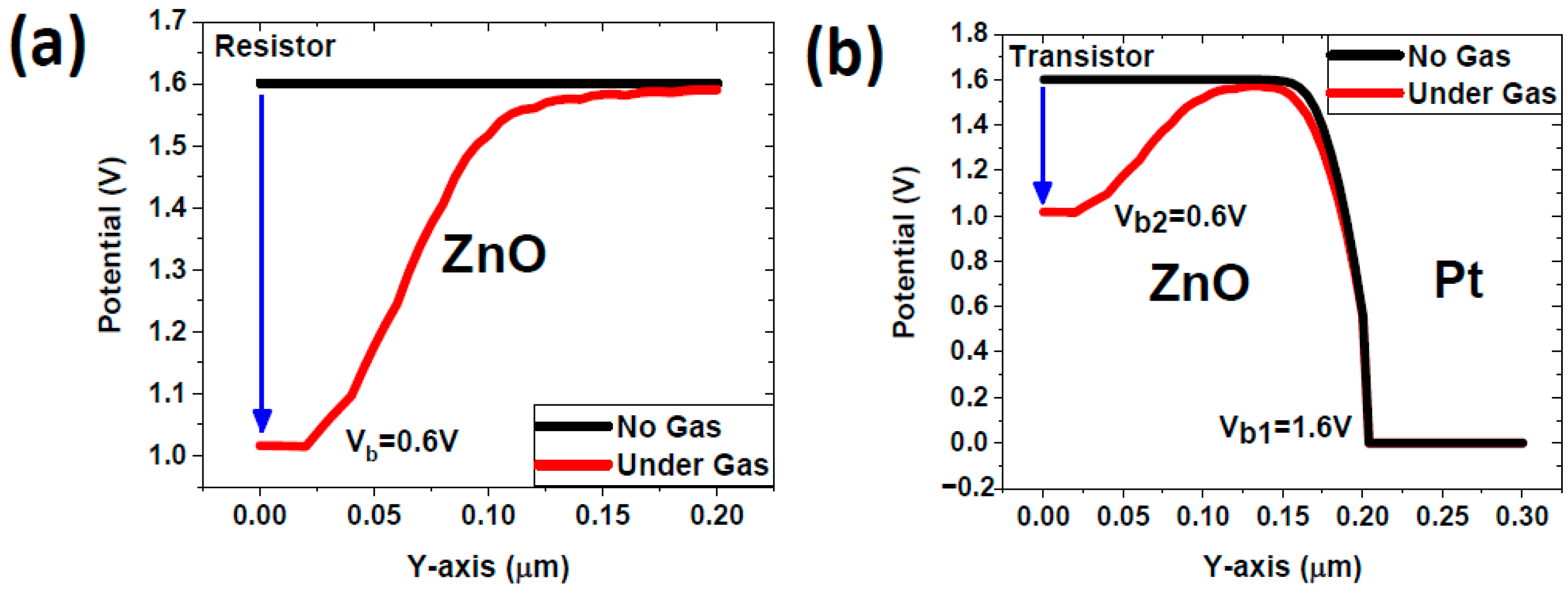
To further analyze this effect, the potential diagrams in Figure 8a,b illustrate the corresponding changes in the electrical potential for the resistor and FGFET gas sensors, respectively. The FGFET structure exhibits a potential barrier of 1.6 V at the interface ZnO/Pt due to the Schottky contact. Upon exposure to NO2, both structures display noticeable alterations in their potential profiles. The interaction with NO2 induces a decrease in the potential, resulting in a potential barrier of 0.6 V for both devices. This change is primarily caused by electron depletion at the ZnO surface, reflecting a reduced free electron concentration due to interactions with NO2 molecules.
As a result, the FGFET structure develops two potential barriers under NO2 exposure, narrowing the conductive channel. This narrowing more effectively restricts the flow of charge carriers compared to the conventional resistor, leading to a greater current reduction, as observed in Figure 6a. This behavior demonstrates that the FGFET architecture provides superior gas sensing performance compared to a standard resistor, making it a more effective choice for detecting gases such as NO2.
To validate the simulation findings, the FGFET and resistive gas sensor structures were also fabricated and experimentally characterized. The comparison between simulated and measured results allows for a comprehensive understanding of the sensor behavior under NO2 exposure.

4.2. Experimental Results

The experimental phase focused on reproducing the sensor structures and exposing them to NO2 gas. By comparing the measured electrical and sensing characteristics with simulation predictions, we aim to validate the enhanced response of the FGFET sensor and its superior sensitivity to NO2. These experimental results will offer further insights into the practical performance of both sensor architectures, supporting the simulation findings.
The ZnO layer was prepared by sputtering a Zn film onto the alumina substrate, followed by thermal oxidation. The color change from gray (metallic Zn) to transparent after oxidation provided an initial qualitative confirmation of ZnO formation. Furthermore, the cross-bar configuration of the sensor enabled clear observation of the distinct layers using SEM analysis. The SEM image in Figure 9a confirmed the presence and separation of the ZnO and Pt layers, validating the successful formation and integration of the ZnO film.
The ZnO layer exhibits a granular morphology with irregularly distributed grains and well-defined pore boundaries (see Figure 9b,c). Its porous nature and high surface-to-volume ratio make the material particularly suitable for gas sensing, promoting efficient adsorption of gas molecules and effective charge carrier transfer.
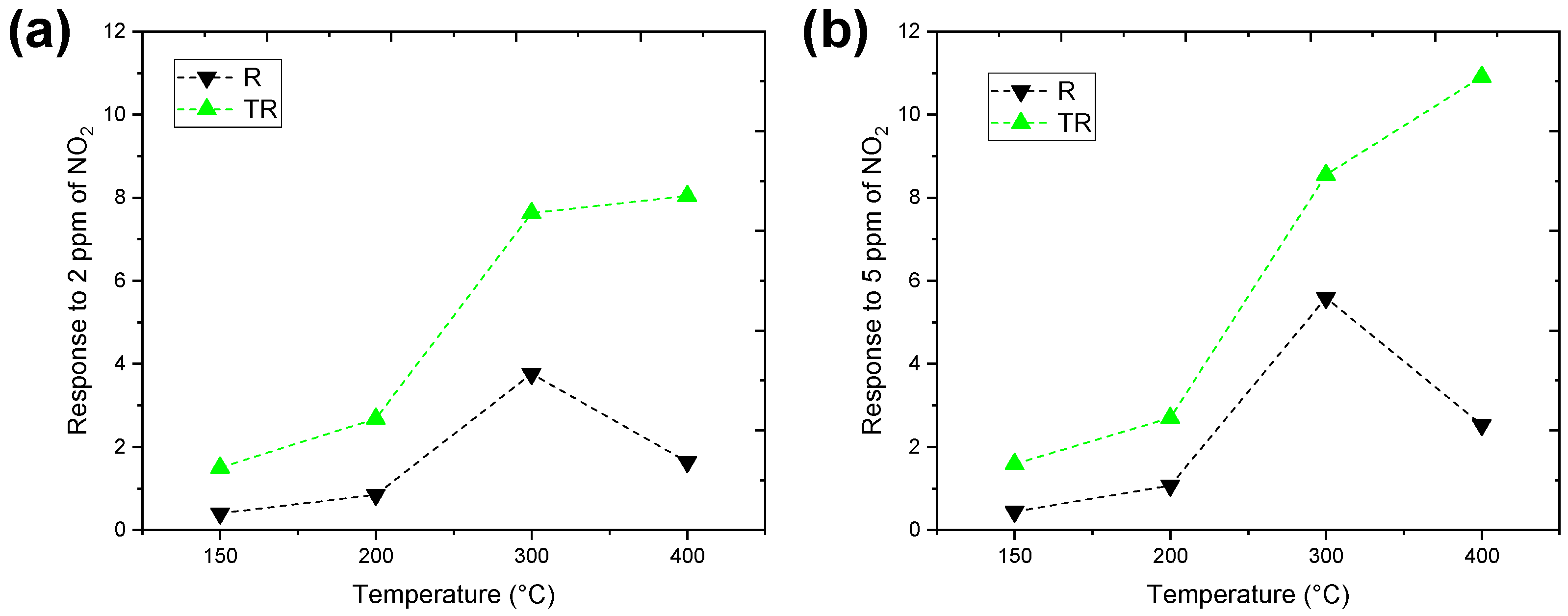
The sensors are tested for low concentrations of NO2 gas at different operating temperatures. Figure 10a,b describe their responses towards 2 ppm and 5 ppm, respectively, showing the highest sensitivities for the FGFET sensors. Unlike the resistor sensor, the TR device exhibits higher responses for NO2 gas detection at different operating temperatures with optimal performance observed at 400 °C.
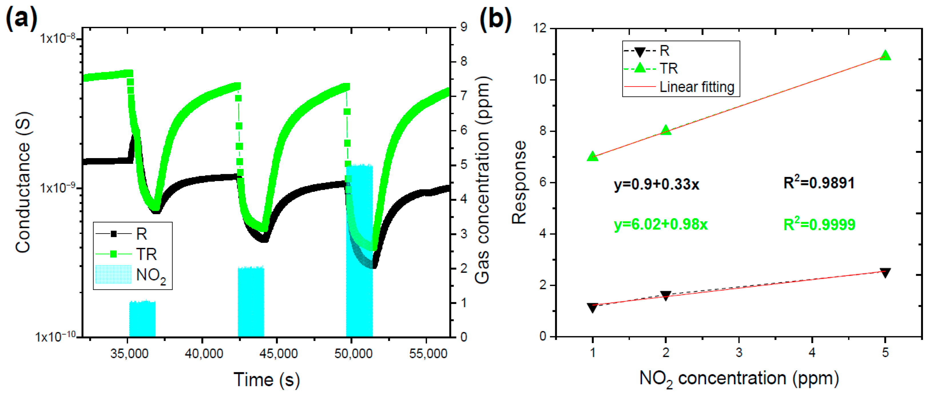
The dynamic response and calibration curves of the sensors to NO2 gas are shown in Figure 11. The observed changes in electrical conductance upon air and gas injection align with the n-type conductivity characteristic of ZnO, as depicted in Figure 11a. Figure 11b shows the calibration performance and sensitivity for R and TR sensors.
The sensing mechanism of ZnO, before and after exposure to NO2, is described above in the simulation part. Additionally, the nanoporous morphology of ZnO further enhances the gas sensing performance by providing abundant pores, which facilitate the diffusion of gas molecules and enlarge the specific surface area, offering more active sites for gas adsorption and reaction. This improves the kinetics of chemical reactions on the surface, leading to a good sensing performance.
The introduction of the Pt layer to ZnO structures to create FGFET devices for NO2 sensing results in the formation of two critical energy or potential barriers that significantly impact the sensor’s performance:
  • Schottky barrier at the ZnO/Pt interface: This barrier arises due to the difference in work function between ZnO and Pt [29]. The Schottky barrier establishes a potential difference that influences charge carrier dynamics within the FGFET structure.
  • Additional barrier due to NO2 interaction: Upon the introduction of NO2 gas, the molecules adsorb onto the ZnO surface, leading to an increase in electron depletion and the formation of an additional potential barrier.
These phenomena are theoretically substantiated and illustrated in Figure 7 and Figure 8. Furthermore, the interplay between these two barriers results in a quantum well formation within the conductive channel of the FGFET. The band bending induced by the Schottky barrier, in conjunction with the electron depletion from NO2 interaction, confines charge carriers within this quantum well. The confinement leads to enhanced charge carrier modulation, amplifying the sensitivity of the sensor to NO2 gas concentrations. As a result, the conductive channel becomes significantly influenced by the concentration of NO2, resulting in a robust sensing signal that accurately reflects environmental NO2 levels, as seen in Figure 11b. The sensitivity magnitude increases with varying the gas concentration from 1 to 5 ppm in a linear fashion with good R-squared values. This linear dependence emphasizes the reliability of our sensors in detecting the oxidizing gas.
The limit of detection (LOD) for NO2 was determined using the standard statistical method based on the signal-to-noise ratio, as defined by the following formula [30]:
L O D = 3 σ α
where σ the standard deviation of the baseline signal (conductance in air) and α is the slope of the calibration curve obtained from the linear fit of sensor response versus NO2 concentration. This approach ensures reliable estimation of the minimum detectable concentration with a 99% confidence level.
A limit of detection value as low as 1 ppm was obtained for the sensors where L O D R = 927   p p b and L O D T R = 89   p p b . These detectable NO2 concentrations meet the Occupational Safety and Health Administration (OSHA) regulations, proving the devices’ efficiency in indoor and environmental monitoring (The LOD values are below the short-term exposure limit STEL = 1 ppm). The TR architecture shows better reliability with 89 ppb as LOD which is less than 100 ppb, recognized as 1-h daily maximum concentrations of NO2 (averaged over 3 years), according to National Ambient Air Quality Standards (NAAQS).
It is noteworthy to highlight that when compared to other studies on ZnO sensors and transistor-based sensors as listed in Table 1, our FGFET device demonstrates superior sensing performance. In another work [5], Andringa et al. demonstrated ZnO FETs operating at 200 °C with a detection limit of ~40 ppb NO2 and response/recovery times of tens to a few hundred seconds. Their devices relied on gate biasing and exhibited incomplete recovery after NO2 removal due to charge trapping at the ZnO/dielectric interface. By contrast, our floating-gate ZnO FETs operate without external gate bias, show stable recovery over repeated cycles, with quantum confinement effects further amplifying the response.
While the highest response obtained for the FGFET sensor is 11 toward 5 ppm of NO2, Pan et al. [43] initially achieved a low response of 1.088 for ZnO nanowires, which was enhanced to a comparable value of 12 using a more complex process to fabricate ZnO hierarchical nanostructures. Their method involved cleaning a silicon wafer with a pre-deposited silicon dioxide layer, spin-coating with photoresist, UV exposure and development, metal deposition, lift-off in acetone, and annealing at 700 °C to form Au nanoparticles. Zn powder was then vaporized and deposited in the presence of an oxygen-argon gas mixture. In contrast, we achieved nearly the same responsiveness using a simpler and more scalable method. By sputtering thin films of Zn (200 nm) and Pt (100 nm) followed by thermal oxidation in air for 1 hour, we were able to produce a nanoporous structure with comparable sensitivity, making our process more suitable for large-scale and industrial applications.
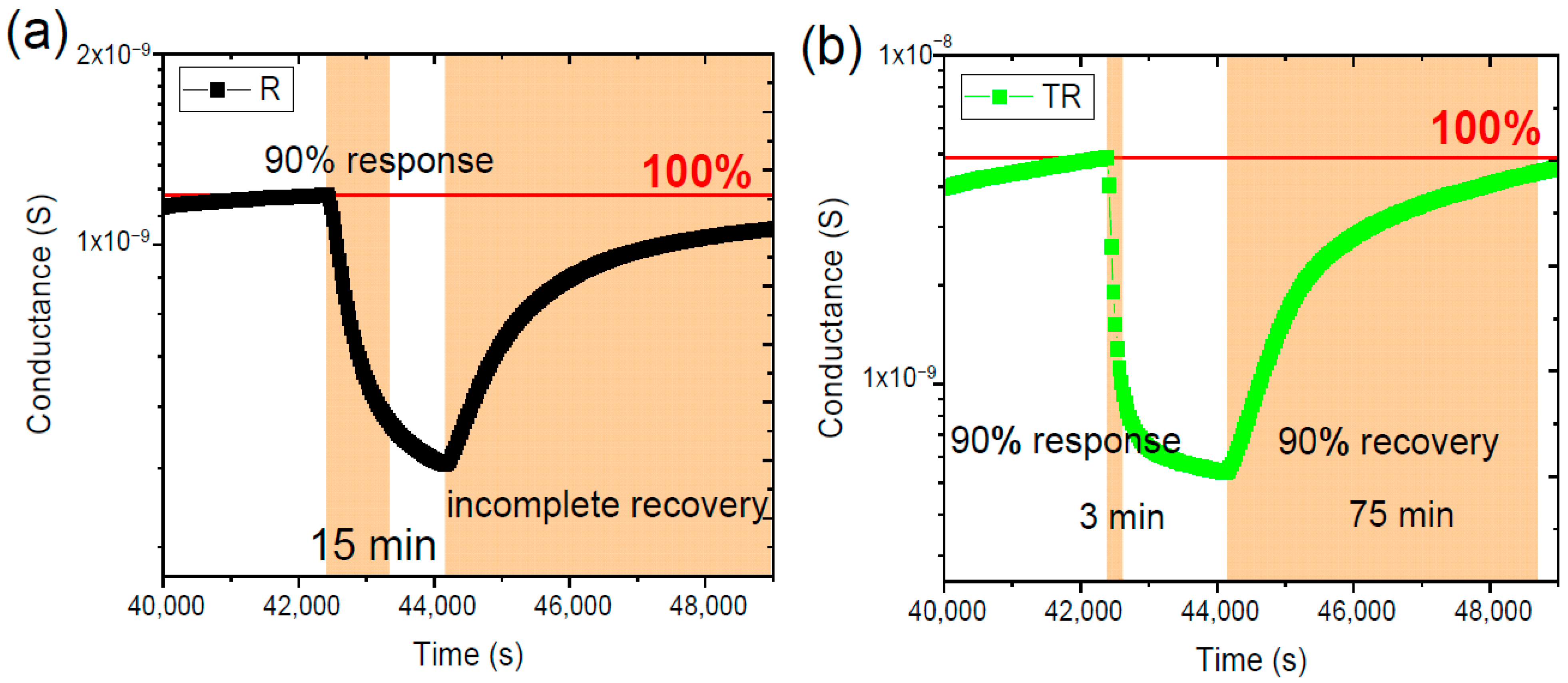
The performance of the FGFET and resistor gas sensors is evaluated in terms of response and recovery times, which are critical parameters for gas sensing applications. Response and recovery times are defined as the time the sensor takes to reach a 90% and 90% change in the total conductance after gas injection and air injection, respectively.
Figure 12 shows the dynamic response-recovery curve of each sensor to 2 ppm NO2 gas at the optimum temperature 400 °C. Since R sensor did not show full reversibility, it was not possible to calculate recovery at 90%.
TR presents shorter response/recovery time of 3/75 min, respectively, compared to the R sensor, which presents 15 min as response time and incomplete recovery. This is due to the enhanced sensing mechanism of the FGFET structure, by the confinement of the charge carrier in the conductive channel which can accelerate the catalytic activity of the sensor. It is worth noting that a chamber with 1L volume was used to locate the sensors. Using a 200 sccm flow it takes 5 min to completely fill and empty the chamber. Therefore, response and recovery times are limited by the volume of the chamber and in case of TR device may be significantly lower.
Besides that, NO2 has strong adsorption to the surface due to the strong binding energy of NO2 molecules and the difference in electron affinity between molecular oxygen (0.4 eV) and NO2 (2.3 eV) which makes the recovery incomplete [12].
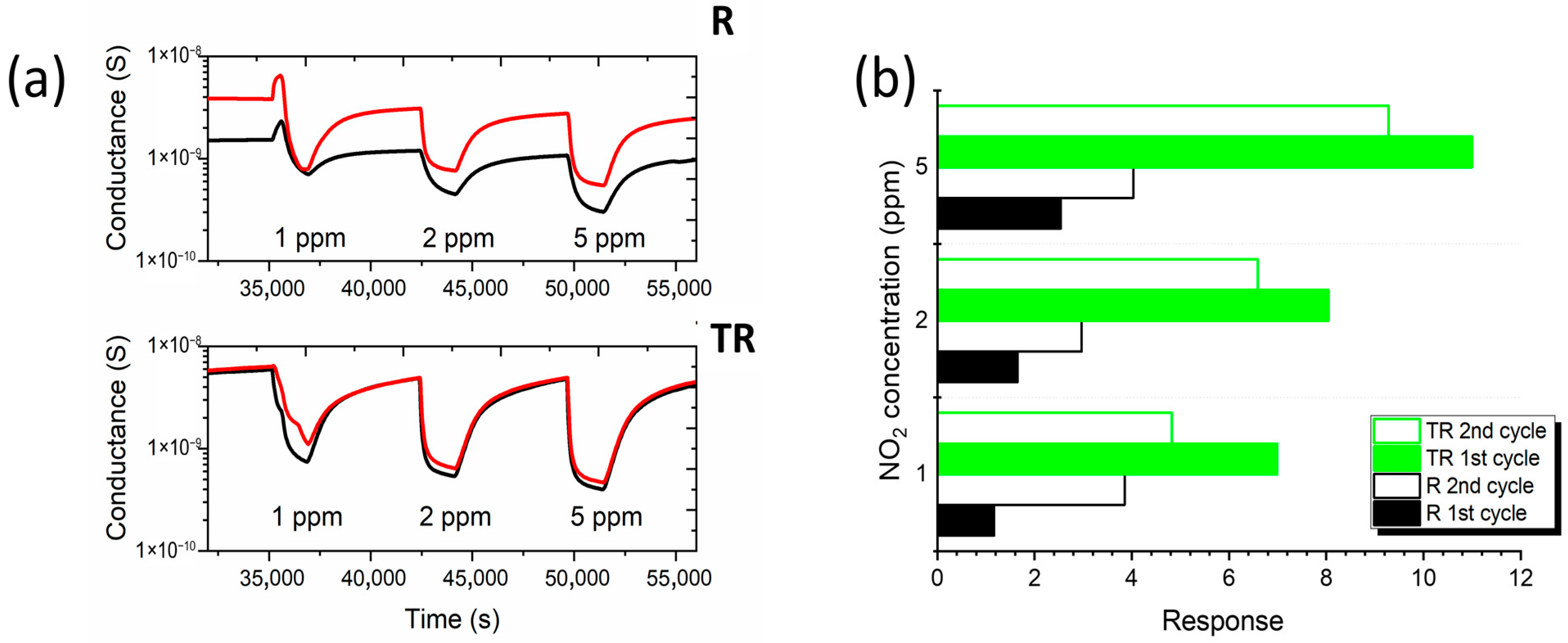
Repeatability in the context of gas sensing performance refers to the ability of a gas sensor to produce consistent and reliable results when exposed to the same concentration of a target gas under identical conditions over multiple tests. In other words, it measures the sensor’s ability to reproduce the same output when the same conditions are applied repeatedly. In Figure 13, the dynamic response of R and TR sensors for 2 cycles is presented (the black line corresponds to the first cycle, while the red line represents the second cycle).
A cycle is defined as one complete air/NO2 exposure/air purge sequence at fixed operating conditions (temperature, relative humidity, and a 1 V DC bias).
One can see the change in baseline conductance for R, accompanied by an increase in response for all concentrations in cycle 2. However, the baseline conductance is still constant for the TR device with a slight decrease in response.
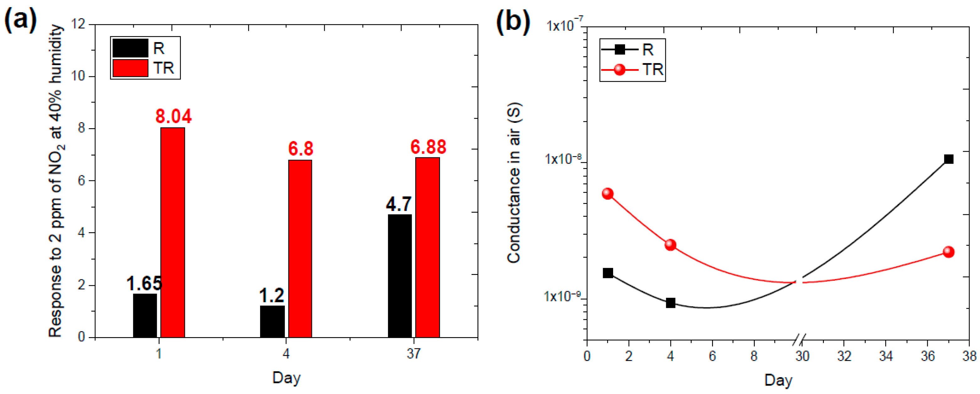
Storage stability is among the important parameters that shape the sensing device’s reliability. Figure 14 shows the response to 2 ppm of NO2 at the same conditions over 37 days.
The sensors exhibit solid stability during the first three days, with R maintaining stability at around 73%, while TR shows even greater stability, holding steady at approximately 85%. The slight decrease in their responses over time may be attributed to the adsorption of atmospheric moisture, which can passivate active surface sites or alter the charge transfer dynamics at the ZnO interface. This phenomenon is consistent with observations reported by Sik Choi et al. [45], who found that the response of their sensors declined from 11.57 to 8.52 after three months of storage due to moisture uptake from the air.
Over prolonged storage in ambient atmosphere, ZnO transistor sensors often suffer from deteriorated response due to moisture and oxygen adsorption, defect-state formation, and carrier trapping. For example, Amna et al. [46] stated that in organic FET-based sensors, exposure to moisture/oxygen during idle periods causes trapping of mobile charges and shifts in threshold voltage, ultimately reducing the drain current and degrading response.
Similarly, studies on ZnO thin-film transistors show that oxygen molecules adsorbed onto surfaces or grain boundaries pull electrons from the conduction channel, increasing the depletion layer and raising baseline resistance (see Figure 14b); this effect reduces the incremental modulation available when the device is exposed to NO2 or other oxidizing gases [47].
However, the pronounced increase in R sensor response after 37 days of storage can be rationalized by considering the effect of long-term moisture adsorption. Previous thermogravimetric studies on tetrapod-shaped ZnO [48] have shown that, under humid conditions, water molecules gradually diffuse into surface cavities and grain boundaries, where they interact with lattice oxygen species to form hydroxyl groups upon heating. The extent of this uptake depends strongly on the relative humidity of the storage environment. During subsequent measurements at operating temperature, the presence of these hydroxyl species modifies the electronic landscape of the sensing film, leading to a shift in its baseline conductivity. In R device, this is manifested as a lower initial resistance before NO2 exposure as shown in Figure 14b. The altered surface chemistry enhances the interaction between ZnO and NO2 molecules, thereby amplifying the response after storage compared with the freshly fabricated sensor.
This interpretation is consistent with the notion that humidity-induced hydroxylation and related surface reconfiguration during storage can activate additional charge-transfer pathways, which become evident as improved sensitivity in later tests.
The different behaviors after storage of the R and TR sensors reflect the influence of device architecture: the TR sensor maintains stability due to channel-dominated operation [49], while the R sensor is directly governed by surface chemistry and defect dynamics, including oxygen vacancy redistribution. The prolonged storage in ambient laboratory conditions may lead to the formation or redistribution of intrinsic defects such as oxygen vacancies, which act as shallow donors in ZnO, thereby increasing the carrier concentration and conductivity with thermal processing [50].
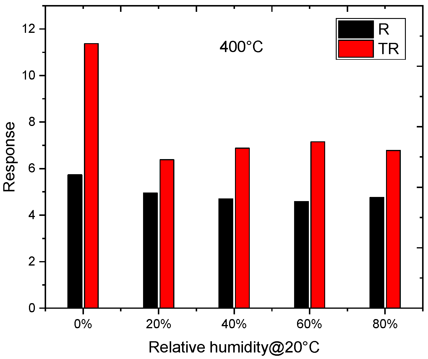
Studying the humidity effect on gas sensing devices is crucial for ensuring their accuracy, reliability, and performance in real-world conditions. It provides valuable insights into how environmental factors influence sensor operation and helps in optimizing sensor design to handle varying humidity levels effectively. Figure 15 describes the gas response of R and TR gas sensors to 2 ppm NO2 gas at 400 °C at different relative humidity.
As can be seen, the sensing response of the sensors exhibits the highest value in the dry environment and decreases with the presence of humidity, noting that transistors demonstrate better response compared to R sensor. This degradation in response is due to water molecules starting to occupy the sensor’s active sites, reducing the availability for NO2 adsorption [51]. The gas response of ZnO-based sensors to NO2 clearly depends on humidity. For the R sensor, the response decreases from 5.73 in dry air (0% RH) to 4.76 at 80% RH, corresponding to a 17% reduction due to water molecules competing with NO2 for adsorption sites and blocking reactive surface regions [52,53]. The TR sensor, while showing a higher dry response (11.37), drops more sharply to 6.78 at 80% RH, a reduction of ~40%, confirming its greater sensitivity to moisture interference.
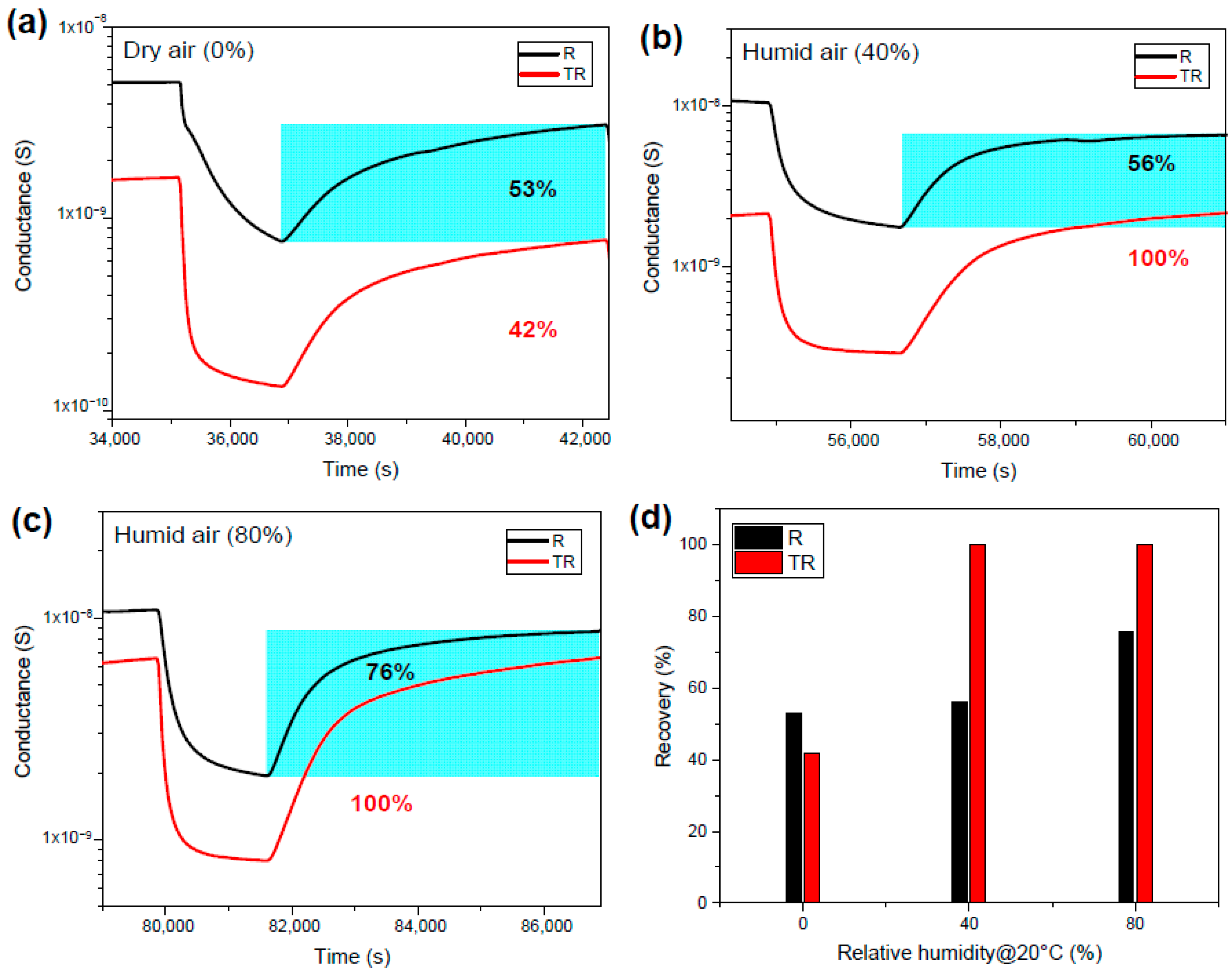
Overall, the presence of water vapor in the environment can interfere with the adsorption of NO2 molecules on the surface of ZnO, leading to a decrease in sensing response. Interestingly, as depicted in Figure 16, humidity has a beneficial impact on sensor performance, particularly in terms of recovery. The recovery is improved under humid air for all devices where TR presents full recovery at higher humidity levels (60% and 80%). This complete recovery of ZnO upon increasing humidity is primarily due to the hydration of the surface and the subsequent desorption of adsorbed gas. Water vapor interacts with the ZnO surface, displacing target gases like NO2, and cleansing the surface.
Other metal–oxide FET sensors have also been explored for NO2 detection. For instance, In2O3-based transistors have achieved sub-ppb detection limits (~0.27 ppb) with rapid response and recovery at relatively low temperatures (75 °C), highlighting their excellent properties when gate bias is optimized [54]. Likewise, WO3 FET employing horizontal floating-gate architecture uses charge-storage engineering to improve recovery and enhance discrimination against interfering gases [6]. Shin et al. have studied FGFET by applying an “erase” bias (ΔV = −2 V) to store excess holes in the floating gate, which raises the electron concentration at the WO3/passivation layer interface. This modulation leads to a 2.4 times larger change in voltage and a 3.2 times increase in sensitivity to NO2 compared to the non-engineered state. Also, recovery speed was improved by applying a pre-bias greater than the read bias. The study explains the enhanced response, sensitivity, and recovery using energy band diagrams, showing how the stored charge increases the density of carriers available for interaction with NO2 molecules, thus amplifying the sensing performance. Compared with these devices, our floating-gate ZnO FET operates without external gate bias, achieves stable recovery and good selectivity under varying humidity, and maintains enhanced sensitivity even after 37 days of storage, confirming its competitiveness among state-of-the-art MOX-FET gas sensors.
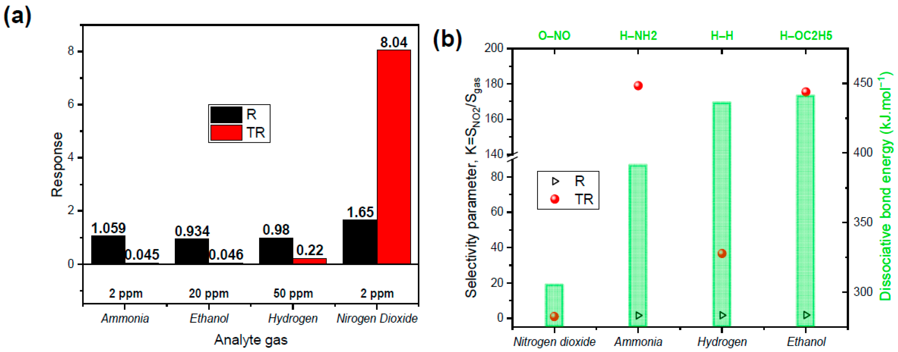
In the field of gas sensing, selectivity refers to the sensor’s ability to preferentially detect a specific target gas in the presence of other gases. A highly selective sensor responds primarily to the target gas with minimal interference or response to other gases in the environment. This property is crucial for accurate detection, as it ensures that the sensor can distinguish the target gas from potentially similar gases or background substances, leading to more reliable and precise measurements. To examine this parameter, we measure the sensitivity of our sensors to different gases shown in Figure 17. As can be seen, TR presents higher selectivity performance than R sensor, which shows very poor selectivity by exhibiting nearly identical responses toward ammonia, ethanol, hydrogen, and nitrogen dioxide.
The selectivity parameters K = S g a s S N O 2 for our sensors (R, TR) reveal significant differences in their ability to preferentially detect NO2 compared to the other gases. For R sensor, the selectivity values indicate that it has a moderate preference for NO2 over ammonia (K = 1.56), ethanol (K = 1.77), and hydrogen (K = 1.69) but the selectivity is not particularly high. In contrast, TR shows exceptionally high selectivity towards NO2 when compared to ammonia and ethanol, with values of 179 and 175, respectively. This indicates a remarkable ability of TR to distinguish NO2 from these gases. In general, the selectivity to NO2 is attributed not only to the high concentration of electron donor sites in the metal oxide [55] and the high electron affinity of NO2, which enables it to effectively withdraw electrons from ZnO and strongly modulate its conductivity, but also to thermodynamic factors related to the low bond dissociation energy of NO2 molecules (see Figure 17b). NO2 molecules possess a relatively low bond dissociation energy (305 kJ/mol), significantly lower than that of common interfering gases such as H2 (436 kJ/mol), NH3 (391 kJ/mol), and ethanol (441 kJ/mol). This means the oxidizing molecules can more readily dissociate and interact with the sensor surface, facilitating efficient adsorption and reaction [56].

5. Conclusions

FET architecture significantly enhances sensitivity, selectivity, stability, and response speed. Both simulation and experimental results confirm that the FET benefits from intrinsic electron confinement and quantum well effects, which amplify the sensing response even without external gate biasing. Moreover, the FET exhibits strong resilience under varying environmental conditions, including changes in humidity, making it a promising candidate for real-world applications such as urban air-quality monitoring, industrial safety, vehicle emission control, and personal exposure assessment. While the relatively high operating temperature may limit scalability due to power and heating requirements, it remains essential for achieving reliable NO2 detection. Future efforts will therefore focus on reducing this constraint through material modification or micro-hotplate integration, paving the way toward next-generation gas sensors that combine high performance with operational simplicity and low power demand.

Author Contributions

Conceptualization, H.H.; methodology, H.H. and H.P.; software, H.H. and Z.B.; validation, D.Z., E.C. and Z.B.; formal analysis, H.H. and M.B.A.; investigation, H.H.; resources, D.Z., E.C. and Z.B.; data curation, H.H. and M.B.A.; writing—original draft preparation, H.H.; writing—review and editing, M.B.A., H.P. and D.Z.; visualization, H.H.; supervision, D.Z. and E.C.; project administration, E.C.; funding acquisition, E.C. All authors have read and agreed to the published version of the manuscript.

Funding

This research was funded by M.U.R. under grant PRIN 2022RWYH2K “Sarcopenia-on-chip: an integrated platform based on chemical sensors, microfluidic devices, and machine learning algorithms for the development and testing of personalized treatment for sarcopenia disease (SELENE)”.

Institutional Review Board Statement

Not applicable.

Informed Consent Statement

Informed consent was obtained from all subjects involved in the study.

Data Availability Statement

The original contributions presented in this study are included in the article. Further inquiries can be directed to the corresponding author.

Conflicts of Interest

The authors declare no conflicts of interest.

References

  1. Khorramifar, A.; Karami, H.; Lvova, L.; Kolouri, A.; Łazuka, E.; Piłat-Rożek, M.; Łagód, G.; Ramos, J.; Lozano, J.; Kaveh, M.; et al. Environmental Engineering Applications of Electronic Nose Systems Based on MOX Gas Sensors. Sensors 2023, 23, 5716. [Google Scholar] [CrossRef]
  2. Gong, H.; Hu, J.; Wang, J.; Ong, C.; Zhu, F. Nano-crystalline Cu-doped ZnO thin film gas sensor for CO. Sens. Actuators B Chem. 2006, 115, 247–251. [Google Scholar] [CrossRef]
  3. Ismail, B.; Abaab, M.; Rezig, B. Structural and electrical properties of ZnO films prepared by screen printing technique. Thin Solid Film. 2001, 383, 92–94. [Google Scholar] [CrossRef]
  4. Shin, H.; Park, J.; Kim, D.; Choi, K.; Park, M.-K.; Hwang, J.; Lee, S.; Joo, Y.-C.; Jung, G.; Lee, J.-H. Optimization of co-sputtered zinc indium tin oxide-based MOSFET-type sensor for effective NO2 gas detection. Sens. Actuators B Chem. 2025, 428, 137262. [Google Scholar] [CrossRef]
  5. Andringa, A.-M.; Piliego, C.; Katsouras, I.; Blom, P.W.M.; Leeuw, D.M.D. NO2 Detection and Real-Time Sensing with Field-Effect Transistors. Chem. Mater. 2014, 26, 773–785. [Google Scholar] [CrossRef]
  6. Shin, W.; Hong, S.; Jeong, Y.; Jung, G.; Park, J.; Kim, D.; Lee, C.; Park, B.-G.; Lee, J.-H. Effect of charge storage engineering on the NO2 gas sensing properties of a WO3 FET-type gas sensor with a horizontal floating-gate. Nanoscale 2021, 13, 9009–9017. [Google Scholar] [CrossRef]
  7. Lee, J.-H. Gas sensors using hierarchical and hollow oxide nanostructures: Overview. Sens. Actuators B Chem. 2009, 140, 319–336. [Google Scholar] [CrossRef]
  8. Yamazoe, N.; Shimanoe, K. Roles of shape and size of component crystals in semiconductor gas sensors: I. Response to oxygen. J. Electrochem. Soc. 2008, 155, J85. [Google Scholar] [CrossRef]
  9. Nagarjuna, Y.; Hsiao, Y.-J.; Wang, S.-C.; Shao, C.-Y.; Huang, Y.-C. Nanoporous ZnO structure prepared by HiPIMS sputtering for enhanced ozone gas detection. Mater. Today Commun. 2023, 35, 106024. [Google Scholar] [CrossRef]
  10. Pleshek, D.; Tran, J.; Li, Y.; Shirani, A.; Shevchenko, E.V.; Berman, D. Swelling-assisted sequential infiltration synthesis of nanoporous ZnO films with highly accessible pores and their sensing potential for ethanol. ACS Appl. Mater. Interfaces 2021, 13, 35941–35948. [Google Scholar] [CrossRef]
  11. Han, S.; Huang, W.; Shi, W.; Yu, J. Performance improvement of organic field-effect transistor ammonia gas sensor using ZnO/PMMA hybrid as dielectric layer. Sens. Actuators B Chem. 2014, 203, 9–16. [Google Scholar] [CrossRef]
  12. Arbia, M.B.; Kim, S.-H.; Yoon, J.-B.; Comini, E. Preparation of NiO NWs by Thermal Oxidation for Highly Selective Gas-Sensing Applications. Sensors 2025, 25, 2075. [Google Scholar] [CrossRef]
  13. Li, M.; Li, B.; Meng, F.; Liu, J.; Yuan, Z.; Wang, C.; Liu, J. Highly sensitive and selective butanol sensors using the intermediate state nanocomposites converted from β-FeOOH to α-Fe2O3. Sens. Actuators B Chem. 2018, 273, 543–551. [Google Scholar] [CrossRef]
  14. Zhang, K.; Qin, S.; Tang, P.; Feng, Y.; Li, D. Ultra-sensitive ethanol gas sensors based on nanosheet-assembled hierarchical ZnO-In2O3 heterostructures. J. Hazard. Mater. 2020, 391, 122191. [Google Scholar] [CrossRef]
  15. Chen, M.; Wang, Z.; Han, D.; Gu, F.; Guo, G. High-sensitivity NO2 gas sensors based on flower-like and tube-like ZnO nanomaterials. Sens. Actuators B Chem. 2011, 157, 565–574. [Google Scholar] [CrossRef]
  16. Qin, W.; Yuan, Z.; Gao, H.; Zhang, R.; Meng, F. Perovskite-structured LaCoO3 modified ZnO gas sensor and investigation on its gas sensing mechanism by first principle. Sens. Actuators B Chem. 2021, 341, 130015. [Google Scholar] [CrossRef]
  17. Gurylev, V.; Perng, T.P. Defect engineering of ZnO: Review on oxygen and zinc vacancies. J. Eur. Ceram. Soc. 2021, 41, 4977–4996. [Google Scholar] [CrossRef]
  18. Sonker, R.K.; Sabhajeet, S.; Singh, S.; Yadav, B. Synthesis of ZnO nanopetals and its application as NO2 gas sensor. Mater. Lett. 2015, 152, 189–191. [Google Scholar] [CrossRef]
  19. Kumar, R.R.; Murugesan, T.; Dash, A.; Hsu, C.-H.; Gupta, S.; Manikandan, A.; Kumar Anbalagan, A.; Lee, C.-H.; Tai, N.-H.; Chueh, Y.-L. Ultrasensitive and light-activated NO2 gas sensor based on networked MoS2/ZnO nanohybrid with adsorption/desorption kinetics study. Appl. Surf. Sci. 2021, 536, 147933. [Google Scholar] [CrossRef]
  20. Yang, Z.; Jiang, L.; Wang, J.; Liu, F.; He, J.; Liu, A.; Lv, S.; You, R.; Yan, X.; Sun, P. Flexible resistive NO2 gas sensor of three-dimensional crumpled MXene Ti3C2Tx/ZnO spheres for room temperature application. Sens. Actuators B Chem. 2021, 326, 128828. [Google Scholar] [CrossRef]
  21. Li, J.; Cai, C.; Li, Z.-H. Knudsen diffusion differs from Fickian diffusion. Phys. Fluids 2021, 33, 042009. [Google Scholar] [CrossRef]
  22. Luo, Y.; Gao, J.; Fu, H.; Liu, S.; Hua, Z. A selective methane gas sensor based on SnO2 utilizing a reactive and porous substrate. Chin. J. Anal. Chem. 2025, 53, 100526. [Google Scholar] [CrossRef]
  23. Sakai, G.; Matsunaga, N.; Shimanoe, K.; Yamazoe, N. Theory of gas-diffusion controlled sensitivity for thin film semiconductor gas sensor. Sens. Actuators B Chem. 2001, 80, 125–131. [Google Scholar] [CrossRef]
  24. Arbia, M.B.; Helal, H.; Saidi, F.; Maaref, H. Investigation of 1.9 μm GINA Simulated as Intrinsic Layer in a GaAs Homojunction: From 25% Towards 32.4% Conversion Yield. J. Electron. Mater. 2020, 49, 6308–6316. [Google Scholar] [CrossRef]
  25. Silvaco International. ATLAS User’s Manual a 2D Numerical Device Simulator, 2004; Silvaco Int.: Santa Clara, CA, USA, 2016. [Google Scholar]
  26. Yang, G.W.; Seo, S.G.; Choi, S.; Kim, D.H.; Jin, S.H. Unscrambling for subgap density-of-states in multilayered MoS2 field effect transistors under DC bias stress via optical charge-pumping capacitance-voltage spectroscopy. IEEE Access 2021, 9, 73090–73102. [Google Scholar] [CrossRef]
  27. De, A.; Karmakar, A.; Ghosh, R.; Saha, P. (Eds.) Investigation of MoS2 based dual gate MOSFET as a H2 sensor considering catalytic metal gate approach. In 2022 IEEE VLSI Device Circuit and System (VLSI DCS); IEEE: New York, NY, USA, 2022. [Google Scholar]
  28. Choi, S.; Seo, S.G.; Yu, H.R.; Kim, S.Y.; Kim, D.H.; Jin, S.H. Hydrophobic Polymer Encapsulation Effects on Subgap Density of States in Multilayered Molybdenum Disulfide Field—Effect Transistors. Phys. Status Solidi (RRL)-Rapid Res. Lett. 2020, 14, 1900492. [Google Scholar] [CrossRef]
  29. Chirakkara, S.; Choudhury, P.R.; Nanda, K.K.; Krupanidhi, S.B. Understanding Pt–ZnO:In Schottky nanocontacts by conductive atomic force microscopy. Mater. Res. Express 2016, 3, 045023. [Google Scholar] [CrossRef]
  30. Franco, M.A.; Conti, P.P.; Andre, R.S.; Correa, D.S. A review on chemiresistive ZnO gas sensors. Sens. Actuators Rep. 2022, 4, 100100. [Google Scholar] [CrossRef]
  31. Modak, M.; Mahajan, S.; Shinde, M.; Rane, S.; Jagtap, S. Sensitive, selective and low detection limit of NO2 gas sensor based on Cu/ZnO/rGO nanocomposites. J. Mater. Sci. Mater. Electron. 2022, 33, 26205–26224. [Google Scholar] [CrossRef]
  32. Jain, S.; Karmakar, N.; Shah, A.; Shimpi, N.G. Development of Ni doped ZnO/polyaniline nanocomposites as high response room temperature NO2 sensor. Mater. Sci. Eng. B 2019, 247, 114381. [Google Scholar] [CrossRef]
  33. Hjiri, M.; Alkaoud, A.; Neri, G. Low operating temperature of UV photo-activated In-doped ZnO NO2 sensors. Appl. Phys. A 2023, 129, 861. [Google Scholar] [CrossRef]
  34. Jaballah, S.; Hjiri, M.; Zahmouli, N.; Albargi, H.B.; Dhahri, R.; Dahman, H.; Mir, L.E.; Neri, G. Room temperature UV-Vis activated NO2 gas sensor-based Mg-doped zinc oxide nanopowders. J. Mater. Sci. Mater. Electron. 2023, 34, 137. [Google Scholar] [CrossRef]
  35. Hjiri, M.; Neri, G. Photo-Activated Ga-ZnO Gas Sensor for NO2 Detection at Near Ambient Temperature. J. Inorg. Organomet. Polym. Mater. 2023, 34, 3374–3383. [Google Scholar] [CrossRef]
  36. Han, T.-H.; Bak, S.-Y.; Kim, S.; Lee, S.H.; Han, Y.-J.; Yi, M. Decoration of CuO NWs Gas Sensor with ZnO NPs for Improving NO2 Sensing Characteristics. Sensors 2021, 21, 2103. [Google Scholar] [CrossRef]
  37. Mun, Y.; Park, S.; An, S.; Lee, C.; Kim, H.W. NO2 gas sensing properties of Au-functionalized porous ZnO nanosheets enhanced by UV irradiation. Ceram. Int. 2013, 39, 8615–8622. [Google Scholar] [CrossRef]
  38. Gonzalez-Chavarri, J.; Parellada-Monreal, L.; Castro-Hurtado, I.; Castaño, E.; Mandayo, G.G. ZnO nanoneedles grown on chip for selective NO2 detection indoors. Sens. Actuators B Chem. 2018, 255, 1244–1253. [Google Scholar] [CrossRef]
  39. Chen, X.; Shen, Y.; Zhang, W.; Zhang, J.; Wei, D.; Lu, R.; Zhu, L.; Li, H.; Shen, Y. In-situ growth of ZnO nanowire arrays on the sensing electrode via a facile hydrothermal route for high-performance NO2 sensor. Appl. Surf. Sci. 2018, 435, 1096–1104. [Google Scholar] [CrossRef]
  40. Vijjapu, M.T.; Surya, S.G.; Yuvaraja, S.; Zhang, X.; Alshareef, H.N.; Salama, K.N. Fully Integrated Indium Gallium Zinc Oxide NO2 Gas Detector. ACS Sens. 2020, 5, 984–993. [Google Scholar] [CrossRef]
  41. Knobelspies, S.; Bierer, B.; Daus, A.; Takabayashi, A.; Salvatore, G.A.; Cantarella, G.; Ortiz Perez, A.; Wöllenstein, J.; Palzer, S.; Tröster, G. Photo-Induced Room-Temperature Gas Sensing with a-IGZO Based Thin-Film Transistors Fabricated on Flexible Plastic Foil. Sensors 2018, 18, 358. [Google Scholar] [CrossRef]
  42. Kim, K.S.; Ahn, C.H.; Jung, S.H.; Cho, S.W.; Cho, H.K. Toward Adequate Operation of Amorphous Oxide Thin-Film Transistors for Low-Concentration Gas Detection. ACS Appl. Mater. Interfaces 2018, 10, 10185–10193. [Google Scholar] [CrossRef] [PubMed]
  43. Pan, X.; Zhao, X.; Chen, J.; Bermak, A.; Fan, Z. A fast-response/recovery ZnO hierarchical nanostructure based gas sensor with ultra-high room-temperature output response. Sens. Actuators B Chem. 2015, 206, 764–771. [Google Scholar] [CrossRef]
  44. Kumar, A.; Jha, P.; Singh, A.; Chauhan, A.K.; Gupta, S.K.; Aswal, D.K.; Muthe, K.P.; Gadkari, S.C. Modeling of gate bias controlled NO2 response of the PCDTBT based organic field effect transistor. Chem. Phys. Lett. 2018, 698, 7–10. [Google Scholar] [CrossRef]
  45. Sik Choi, M.; Young Kim, M.; Mirzaei, A.; Kim, H.-S.; Kim, S.-i.; Baek, S.-H.; Won Chun, D.; Jin, C.; Hyoung Lee, K. Selective, sensitive, and stable NO2 gas sensor based on porous ZnO nanosheets. Appl. Surf. Sci. 2021, 568, 150910. [Google Scholar] [CrossRef]
  46. Amna, B.; Ozturk, T. Organic field-effect transistor-based sensors: Recent progress, challenges and future outlook. J. Mater. Chem. C 2025, 13, 8354–8424. [Google Scholar] [CrossRef]
  47. Khan, N.D. An Investigation of the Performance and Stability of Zinc Oxide Thin-Film Transistors and the Role of High-k Dielectrics. Ph.D. Thesis, De Montfort University, Leicester, UK, 2010. [Google Scholar]
  48. Bai, Z.; Xie, C.; Hu, M.; Zhang, S.; Zeng, D. Effect of humidity on the gas sensing property of the tetrapod-shaped ZnO nanopowder sensor. Mater. Sci. Eng. B 2008, 149, 12–17. [Google Scholar] [CrossRef]
  49. Shin, W.; Jung, G.; Hong, S.; Jeong, Y.; Park, J.; Kim, D.; Jang, D.; Kwon, D.; Bae, J.-H.; Park, B.-G.; et al. Proposition of deposition and bias conditions for optimal signal-to-noise-ratio in resistor- and FET-type gas sensors. Nanoscale 2020, 12, 19768–19775. [Google Scholar] [CrossRef]
  50. Feng, W.-W.; Cho, S.; Wang, M.-S.; Dung, D.D. Co-contribution of hydrogen impurities and native defects might be the answer for the n-type conductivity in ZnO. Phys. Lett. A 2016, 380, 480–484. [Google Scholar] [CrossRef]
  51. Wang, J.; Shen, Y.; Li, X.; Xia, Y.; Yang, C. Synergistic effects of UV activation and surface oxygen vacancies on the room-temperature NO2 gas sensing performance of ZnO nanowires. Sens. Actuators B Chem. 2019, 298, 126858. [Google Scholar] [CrossRef]
  52. Ben Arbia, M.; Helal, H.; Comini, E. Recent Advances in Low-Dimensional Metal Oxides via Sol-Gel Method for Gas Detection. Nanomaterials 2024, 14, 359. [Google Scholar] [CrossRef]
  53. Kaneti, Y.V.; Yue, J.; Jiang, X.; Yu, A. Controllable synthesis of ZnO nanoflakes with exposed (1010) for enhanced gas sensing performance. J. Phys. Chem. C 2013, 117, 13153–13162. [Google Scholar] [CrossRef]
  54. Yeom, G.; Kwon, D.; Shin, W.; Park, M.-K.; Kim, J.-J.; Lee, J.-H. Fast-response/recovery In2O3 thin-film transistor-type NO2 gas sensor with floating-gate at low temperature. Sens. Actuators B Chem. 2023, 394, 134477. [Google Scholar] [CrossRef]
  55. Marikutsa, A.; Rumyantseva, M.; Konstantinova, E.A.; Gaskov, A. The Key Role of Active Sites in the Development of Selective Metal Oxide Sensor Materials. Sensors 2021, 21, 2554. [Google Scholar] [CrossRef] [PubMed]
  56. Pakdel, H.; Borsi, M.; Ponzoni, M.; Comini, E. Enhanced Gas Sensing Performance of CuO-ZnO Composite Nanostructures for Low-Concentration NO2 Detection. Chemosensors 2024, 12, 54. [Google Scholar] [CrossRef]
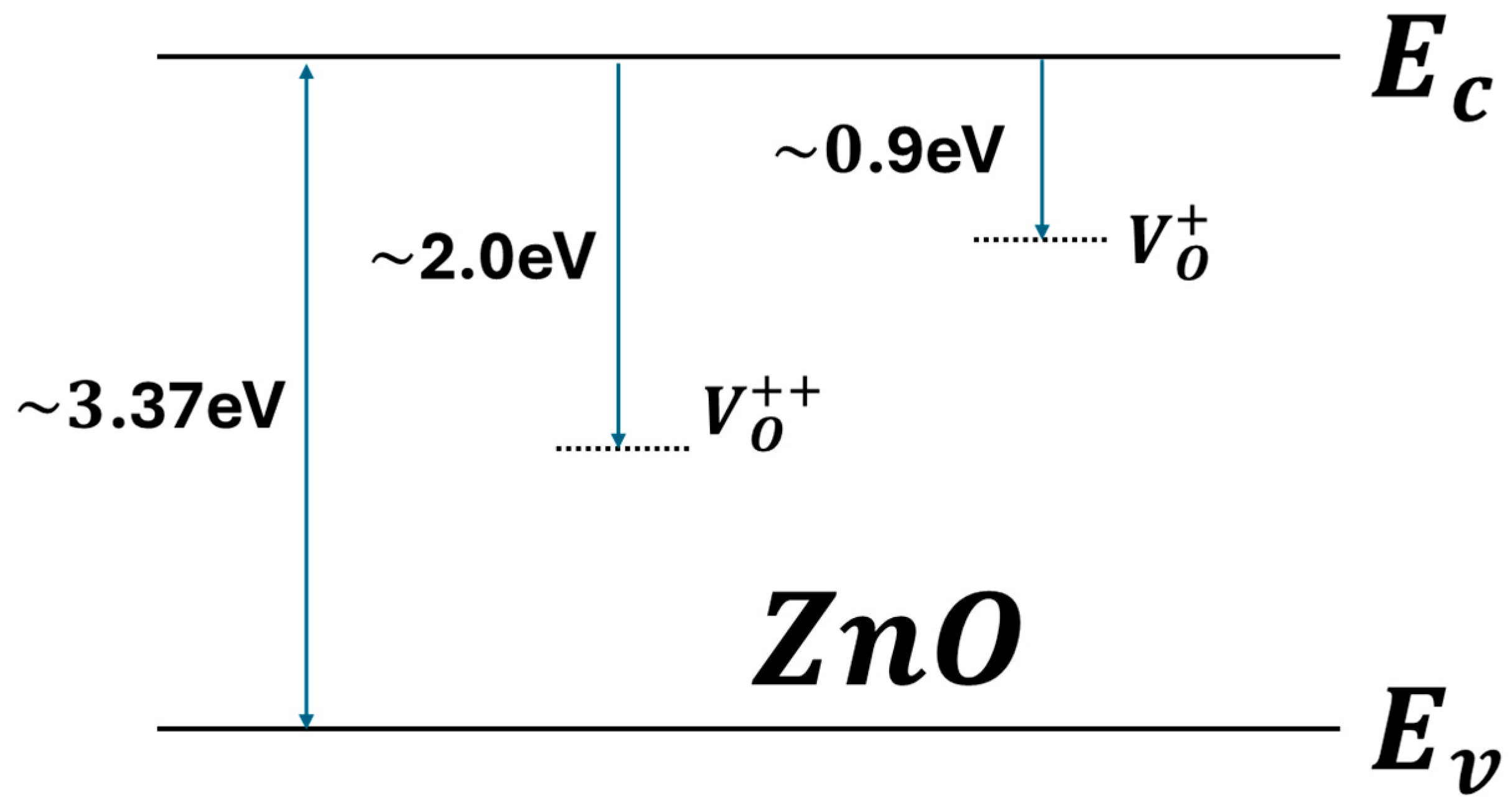
Figure 1. Energy band gap of ZnO with energy levels of oxygen vacancies V O + and V O + + .
Chemosensors 13 00358 g001
Figure 2. (a) Schematic illustration of a porous thin film exposed to gas flow. (b) Simulated Gas diffusion profile across sensing layer depth at different m values.
Chemosensors 13 00358 g002
Figure 3. Graphic structure of the resistor (a) and FGFET (b) based gas sensors.
Chemosensors 13 00358 g003
Figure 4. Top and bottom view of the sensor configuration (Transistor).
Chemosensors 13 00358 g004
Figure 5. Schematic illustration of sensors’ fabrication.
Chemosensors 13 00358 g005
Figure 6. (a) Current versus applied voltage before and after exposure to NO2 and (b) gas sensing response of the resistor and FGFET devices toward NO2.
Chemosensors 13 00358 g006
Figure 7. Energy band profile of the (a) resistor- and (b) FGFET-based gas sensors, along the y-axis.
Chemosensors 13 00358 g007
Figure 8. Potential diagram of the resistor (a) and FGFET (b) based gas sensors, along the y-axis. Blue arrows indicate the potential change after gas exposure.
Chemosensors 13 00358 g008
Figure 9. SEM images of ZnO structure (a) on Pt (b) and on alumina substrate (c).
Chemosensors 13 00358 g009
Figure 10. Gas response of the resistor and FGFET sensors at different operating temperatures to (a) 2 ppm and (b) 5 ppm of NO2 gas at 40% of relative humidity@20 °C.
Chemosensors 13 00358 g010
Figure 11. (a) The dynamic response-recovery curves of ZnO sensors to 1–5 ppm NO2 gas at 400 °C and 40% of relative humidity@20 °C. (b) The linear fitting curve to relative response in (a).
Chemosensors 13 00358 g011
Figure 12. Dynamic response to 2 ppm NO2 gas at 400 °C and 40% of relative humidity@20 °C for (a) resistor and (b) transistor devices.
Chemosensors 13 00358 g012
Figure 13. (a) Repeatability performance to NO2 gas at 400 °C and 40% of relative humidity@20 °C: cycle 1 (black line) and cycle 2 (red line). (b) Histogram representation of sensitivity extracted from (a): filled rectangles and empty rectangles describe the first and second cycles, respectively.
Chemosensors 13 00358 g013
Figure 14. (a) Storage stability performance to 2 ppm NO2 gas at 400 °C and 40% of relative humidity@20 °C. (b) Baseline conductance evolution of the sensors over 37 measurement days.
Chemosensors 13 00358 g014
Figure 15. Response dependency on relative humidity levels at 400 °C, under exposure to 2 ppm NO2.
Chemosensors 13 00358 g015
Figure 16. Dynamic response-recovery curves to 2 ppm in dry (a) and humid (bc) environments with (d) representative histogram of recovery dependency on humidity levels at 400 °C.
Chemosensors 13 00358 g016
Figure 17. (a) Gas response of the ZnO sensor at 400 °C and 40% RH. Responses were recorded at the concentrations indicated in the legend. (b) Selectivity factor, defined as the response to each gas normalized to the response to NO2. Empty triangles correspond to the R sensor, while red circles represent the TR sensor. The bond-dissociation energy values for the relevant bonds are represented as green histograms for comparison.
Chemosensors 13 00358 g017
Table 1. Summary of previously reported metal oxide-based gas sensors and transistors to 5 ppm of NO2.
Device TypeSubstrateSensing LayerSensing ConditionResponseLOD (ppb)References
Conductometric sensorAluminaZnO thin film400 °C2.54 (1)927Present work
Resistive sensorAluminaZnO film250 °C1.42 (2)NA *[31]
Resistive sensorGlassNi-doped ZnO/PANi nanocompositeRT **0.14 (3)NA[32]
Resistive sensorAluminaZnO100 °C, under UV exposure  <1.5 (2)NA[33]
Resistive sensorAluminaMg-doped ZnO400 °C
30 °C, under UV exposure
1.01 (2)
≈1.5 (2)
NA
NA
[34]
Resistive sensorAluminaZnO300 °C, under UV exposure1.5 (2)NA[35]
Resistive sensorNAZnO NPs decorated on CuO NWs250 °C1.17 (4)NA[36]
Resistive sensorOxidized Si substrate ZnO nanosheetsRT, under UV exposure (1.2 mW/cm2)≈1.37 (2)NA[37]
Resistive sensorOxidized Si substrate Au-functionalized ZnO nanosheetsRT, under UV exposure (0.35 mW/cm2)
RT, under UV exposure (1.2 mW/cm2)
≈1.33 (2)
≈4.55 (2)
NA
NA
[37]
Resistive sensorAluminaZnO nanoneedles195 °C1.04 (5)80[38]
Resistive sensorAluminaZnO Nanowires250 °C3.3 (2)NA[39]
Thin Film TransistorPt/AluminaZnO thin film400 °C11 (1)89Present work
Thin Film TransistorSiO2/SiIndium Gallium Zinc Oxide thin filmRT−0.998 (6)100[40]
Thin Film Transistor Flexible Plastic FoilIndium Gallium Zinc Oxide thin filmRT<1.5 (7)NA[41]
Thin Film TransistorSiO2/SiIndium Gallium Zinc Oxide thin film100 °C<4 (8)NA[42]
Thin Film TransistorSilicon chipZnO nanowiresRT1.088 (2)NA[43]
Organic Field Effect TransistorBOPETPCDTBT polymerRT≈0.5 (6)1000[44]
* NA: not available, ** RT: room temperature. (1)  S = G g a s G a i r G a i r , (2)  S = R g a s R a i r , (3)  S = R g a s R a i r R g a s , (4)  S = R a i r R g a s , (5)  S = R g a s R a i r R a i r , (6)  S = I g a s I a i r I a i r , (7)  S = I a i r I g a s , (8)  S = d l o g I g a s d t d l o g I a i r d t d l o g I a i r d t .
Disclaimer/Publisher’s Note: The statements, opinions and data contained in all publications are solely those of the individual author(s) and contributor(s) and not of MDPI and/or the editor(s). MDPI and/or the editor(s) disclaim responsibility for any injury to people or property resulting from any ideas, methods, instructions or products referred to in the content.