Article

Layer-by-Layer Film Based on Sn3O4 Nanobelts as Sensing Units to Detect Heavy Metals Using a Capacitive Field-Effect Sensor Platform

by
Paulo V. Morais
1,2,
Pedro H. Suman
1,
Michael J. Schöning
3,4,
José R. Siqueira, Jr.
2,* and
Marcelo O. Orlandi
1
1
Department of Engineering, Physics and Mathematics, Institute of Chemistry, São Paulo State University (UNESP), Araraquara 14800-060, SP, Brazil
2
Laboratory of Applied Nanomaterials and Nanostructures (LANNA), Institute of Exact Sciences, Natural and Education, Federal University of Triângulo Mineiro (UFTM), Uberaba 38064-200, MG, Brazil
3
Institute of Nano- and Biotechnologies (INB), FH Aachen, Campus Jülich, 52428 Jülich, Germany
4
Institute of Biological Information Processing (IBI-3), Forschungszentrum Jülich, 52425 Jülich, Germany
*
Author to whom correspondence should be addressed.
Chemosensors 2023, 11(8), 436; https://doi.org/10.3390/chemosensors11080436
Submission received: 29 June 2023 / Revised: 21 July 2023 / Accepted: 2 August 2023 / Published: 5 August 2023

Abstract

:
Lead and nickel, as heavy metals, are still used in industrial processes, and are classified as “environmental health hazards” due to their toxicity and polluting potential. The detection of heavy metals can prevent environmental pollution at toxic levels that are critical to human health. In this sense, the electrolyte–insulator–semiconductor (EIS) field-effect sensor is an attractive sensing platform concerning the fabrication of reusable and robust sensors to detect such substances. This study is aimed to fabricate a sensing unit on an EIS device based on Sn3O4 nanobelts embedded in a polyelectrolyte matrix of polyvinylpyrrolidone (PVP) and polyacrylic acid (PAA) using the layer-by-layer (LbL) technique. The EIS-Sn3O4 sensor exhibited enhanced electrochemical performance for detecting Pb2+ and Ni2+ ions, revealing a higher affinity for Pb2+ ions, with sensitivities of ca. 25.8 mV/decade and 2.4 mV/decade, respectively. Such results indicate that Sn3O4 nanobelts can contemplate a feasible proof-of-concept capacitive field-effect sensor for heavy metal detection, envisaging other future studies focusing on environmental monitoring.

Graphical Abstract

1. Introduction

Identifying and detecting heavy metals in water, soil, and the atmosphere is highly relevant to environmental monitoring, safety, and food quality control. Among the 35 metals found in nature, 23 are considered heavy metals due to their intrinsic properties, including high atomic weight, density, and tensile strength [1,2]. Heavy metals are nonbiodegradable materials with high toxicity to human health due to metal bond formation with the thiol group of proteins [3,4,5]. Lead (Pb) is an element used in the manufacturing process of various products, including paints, ammunition, solder, pipes, and batteries. However, lead water pollution is one of the most worrisome, and the United States Environmental Protection Agency (EPA) and the World Health Organization (WHO) have reported lead concentration limits in drinking water of 0.072 μmol/L (15 µg/L) and 0.048 μmol/L (10 µg/L), respectively [6,7]. Also, this heavy metal is considered an “environmental health hazard” compound ranked in the top 10 on the Substance Priority List of the Agency for Toxic Substances and Disease Registry (ATSDR) based on its toxicity and potential for air, water, and soil contamination in the ionic state (Pb2+) [3].
Nickel (Ni) is a lustrous and silvery toxic metal easily found in the Ni0 or Ni2+ states in wastewater from industrial machine components, electronics, jewelry, stainless steel kitchen utensils, dental or orthopedic implants, coins, and magnets [8,9]. Due to its bio-accumulation capacity, wastewater containing high Ni concentrations can pollute plants, which leads to contamination risks from food consumption by humans and animals. The nickel potential as an immunotoxin, immunomodulatory allergen, and carcinogenic agent can affect a person’s health [8,9]. Regarding nickel pollution in water, the EPA recommends Ni levels less than 1.7 µmol/L (0.1 mg/L) in drinking water [10]. Furthermore, the reference amounts for nickel in serum and urine reported by the WHO are 0.2 μg/L and 1–3 μg/L [11].
The combination of nanomaterials in field-effect devices (FEDs) allows the integration of sensor arrays on a single chip favoring the development of sensitive, smaller, low-weight, and low-cost devices. In this sense, the electrolyte–insulator–semiconductor (EIS) field-effect capacitor is a simple and robust sensing platform for detecting heavy metals. The layer-by-layer (LbL) method can be employed to modify an EIS surface by incorporating nanomaterials (e.g., metal oxides) arranged with polyelectrolytes to form specific sensing units (receptor layers). This method is advantageous as the correct choice and combination of materials incorporated on the chip may lead to EIS sensors with improved properties in terms of sensitivity, limit of detection, and output signal response [12,13,14,15]. For example, EIS devices modified with LbL films containing ZnO [16] and CoFe2O4 [17,18] materials have recently demonstrated enhanced properties for detecting inorganic and organic substances.
Other employed nanomaterials for modifying EIS devices using the LbL technique may result in promising new devices. In particular, tin dioxide (SnO2)-based materials have been extensively used in various applications, such as gas sensors [19] and anode material in lithium-ion batteries [20,21], owing to their excellent optoelectronic properties and chemical sensitivity. In addition, some works have also reported the application of SnO2 for the detection and adsorption of heavy metals [22,23,24]. However, unusual stoichiometries of tin oxide are still poorly studied, which may be related to challenges in the synthesis process of this nanomaterial. As a variant, Sn3O4 represents a mixed-valence tin oxide exhibiting n-type conductivity and a bandgap of ~2.6 eV. On the other hand, Sn3O4 has been exploited in limited applications, including gas sensors and photocatalysts [19,25,26,27,28]. Thus, there is a wide range of possibilities for further investigations on Sn3O4 materials considering the larger surface area and specific properties, such as chemical structure with two oxidation states, energy gap in the visible portion of the electromagnetic spectrum, and great stability at temperatures lower than 723 K [29]. In this context, the incorporation of sensing layers over EIS chips by combining Sn3O4 nanobelts with polyelectrolytes (e.g., polyallylamine hydrochloride (PAH), polyacrylic acid (PAA), and polyvinylpyrrolidone (PVP)) using the LbL method is a suitable alternative to achieve a heavy metal sensor with improved properties.
This work reports the fabrication of EIS devices modified with an LbL film by combining Sn3O4 nanobelts complexed with polyacrylic acid (PAA) alternated with a polyvinylpyrrolidone (PVP) polyelectrolyte for Pb2+ and Ni2+ ion detection. The surface of the LbL film was characterized by SEM (scanning electron microscopy) analyses, and electrochemical studies were performed using capacitance–voltage (C–V) and constant capacitance (ConCap) measurements. To the best of our knowledge, this system, based on an LbL film containing Sn3O4 nanobelts, is the first report on Pb2+ and Ni2+ ion detection contemplating a proof-of-concept capacitive field-effect sensor for environmental monitoring and sensing applications.

2. Materials and Methods

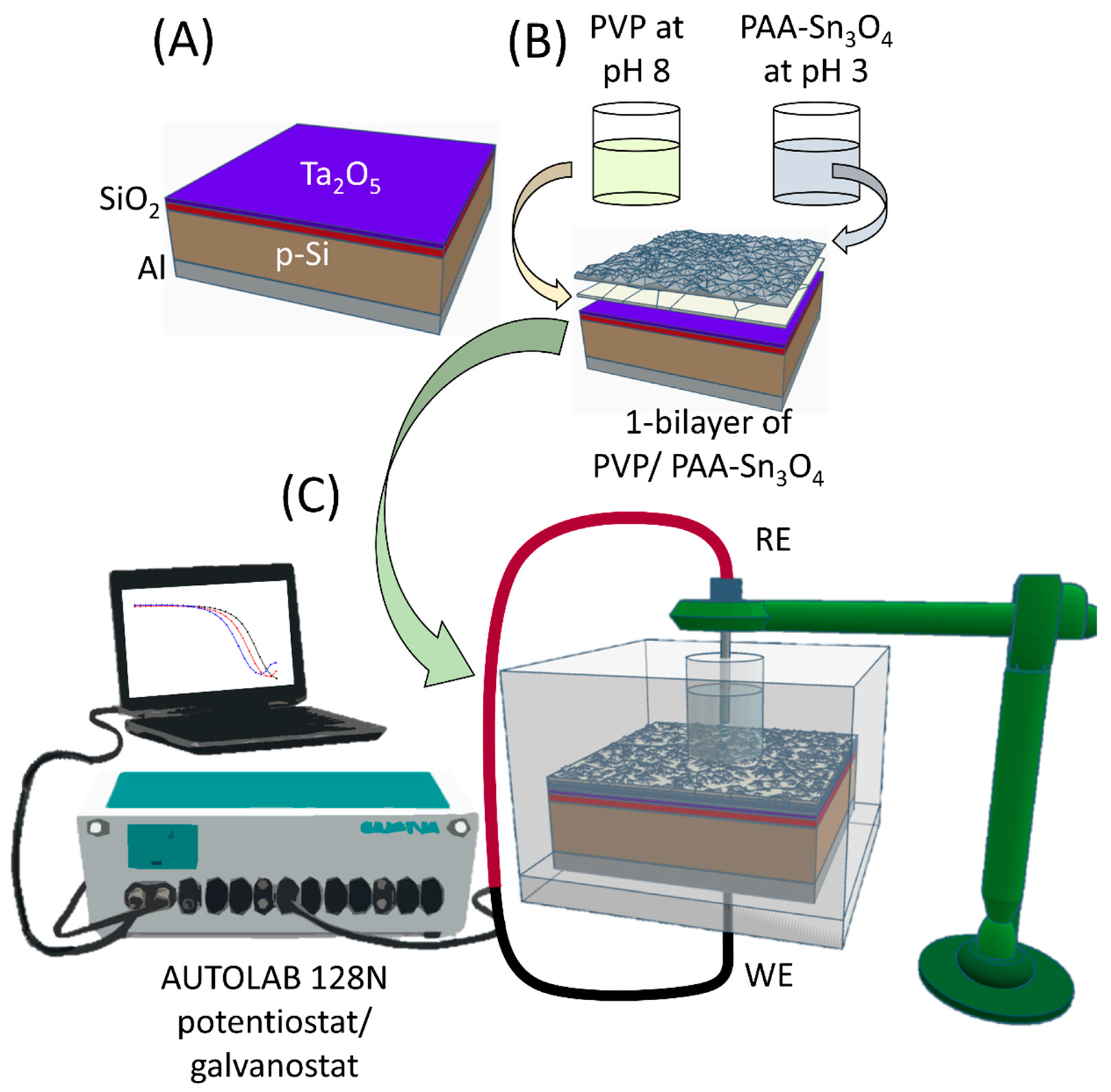
2.1. Synthesis of Sn3O4 Nanobelts

Sn3O4 nanobelts were synthesized from the carbothermal reduction method according to experimental parameters previously reported [25]. In brief, SnO2 (Sigma-Aldrich, St. Louis, MO, USA, 99.9% purity) and carbon black (Union Carbide, Houston, TX, USA, >99% purity) powders were mixed, followed by heating at 1135 °C in a tubular furnace with a controlled synthesis atmosphere. The obtained Sn3O4 nanobelts were analyzed by X-ray diffraction (XRD, Shimadzu, Kyoto, Japan, model XRD 6000), field-emission scanning electron microscopy (FE-SEM, JEOL, Tokyo, Japan, model 7500F), high-resolution transmission electron microscopy (HR-TEM, Philips, Netherlands, model CM200), and specific surface area by the Brunauer–Emmett–Teller (BET, Philips, Netherlands, model CM200) method (see results in references [25,30]).

2.2. Fabrication of the EIS Chips

EIS chips with a p-Si-SiO2-Ta2O5 structure were fabricated according to a well-established method reported by Schöning and coworkers [31]. In summary, the chip production is based on the following processes: (i) the SiO2 insulating layer with a 30 nm thick is formed by thermal oxidation under O2 atmosphere at 1050 °C for 30 min on a p-doped 〈100〉 silicon wafer substrate (356–406 µm thick) with a specific resistance of ρ = 1–5 Ω·cm; (ii) a 30 nm Ta layer is deposited on top of the SiO2 layer via electron beam evaporation, followed by thermal oxidation in an oxygen atmosphere at 520 °C for 2 h to form a pH-sensitive Ta2O5 film with a thickness of ca. 60 nm; (iii) on the rear side of the p-Si, a contact layer of Al film with a thickness of 300 nm is electron beam evaporated; (iv) finally, the wafer is cut into single chips of 1 cm × 1 cm sizes.

2.3. Fabrication and Characterization of the LbL Films

Polyacrylic acid (PAA, 25 wt% solution in water; Alfa Aesar, Haverhill, MA, USA) and polyvinylpyrrolidone (PVP, MW = 40,000 g/mol; Sigma Aldrich) were used for the fabrication of the LbL film. PAA and PVP solutions with concentrations of 1 mg/mL were prepared using ultrapure deionized water, and their pHs were adjusted to 3 and 8, respectively. In sequence, 7.5 mg of Sn3O4 nanobelts were dispersed in 10 mL of PAA solution in an ultrasonic tip DES500 (Unique Group, Rio de Janeiro, Brazil) using 500 Watts of ultrasonic power for 3 min, reaching a stable dispersion.
The LbL film was fabricated in duplicate and deposited on top of the electrolyte–insulator–semiconductor (EIS) sensor with a p-Si-SiO2-Ta2O5 structure (Figure 1A) measuring 1 cm2 in size. Figure 1B shows a representation of the LbL film sandwich. First, the EIS device surface was cleaned with acetone, followed by ethanol and ultrapure deionized water in an ultrasonic bath for 5 min at each step. Then, the sensor chip was inserted in a homemade, acrylic, O-ring-sealed electrochemical measuring cell used as a template. Subsequently, 500 µL of the PVP solution and the PAA-Sn3O4 dispersion were dropped into the reservoir over the chip alternately for 10 min. After each deposition, the liquid was removed, and the chip was rinsed with deionized water and dried with nitrogen. This process resulted in 1 bilayer with a PVP/PAA-Sn3O4 structure. Using this procedure, a pair of LbL films containing 5 bilayers was fabricated and named EIS-Sn3O4. The morphological characteristics of the EIS-Sn3O4 device surface were studied using field-emission scanning electron microscopy (FE-SEM; JEOL (Tokyo, Japan), model 7500F).

2.4. Electrochemical Characterization for Pb2+ and Ni2+ Ion Detection

The electrochemical measurements were performed three times for the duplicated set of EIS sensors using an impedance analyzer AUTOLAB 128N potentiostat/galvanostat (MetrohmAutoLab, Utrecht, Switzerland) controlled by NOVA software version 1.11. The sensor chip is mounted in a homemade, acrylic, O-ring-sealed measurement cell connected to an Ag/AgCl double-junction (3 M KCl) reference electrode (RE) (Metrohm, Switzerland), which is inserted into the analyte solution that is in contact with the outermost bilayer of the PVP/PAA-Sn3O4 LbL film; the sensor chip serves as working electrode (WE), as shown in the scheme in Figure 1C. Standard buffer solutions at pH 4, 7, and 10 were purchased from SpeeSol (Brazil) for electrochemical characterization. Capacitance–voltage (C–V) measurements were performed in each buffer solution in a potential range of −2.0 V to 0.6 V (vs. Ag/AgCl). Using the flat band region from the C–V curves, constant capacitance (ConCap) curves were obtained by monitoring the output potential around 40 nF from successive C–V measurements lasting 8 min from pH 10 to pH 4. Nickel and lead ion solutions were prepared using nickel nitrate (Ni(NO3)2.6H2O; Sigma Aldrich) and lead acetate (Pb(C2H3O2)2.3H2O; Synth) in phosphate buffer solution (PBS, pH 7) with concentrations ranging from 2.4 μM to 482 μM for Pb2+ ions and 8.5 μM to 426 μM for Ni2+ ions. First, C–V measurements were carried out from −2.0 V to 0.6 V. Then, dynamic constant capacitance (ConCap) analyses were performed by monitoring the output potential for 5 min, considering the flat band region around 43–40 nF. Calibration curves were generated using the ConCap curves, and the sensitivities toward the Pb2+ and Ni2+ ions were calculated taking the average values from their calibration curves for a duplicate set of bare and modified EIS sensors.

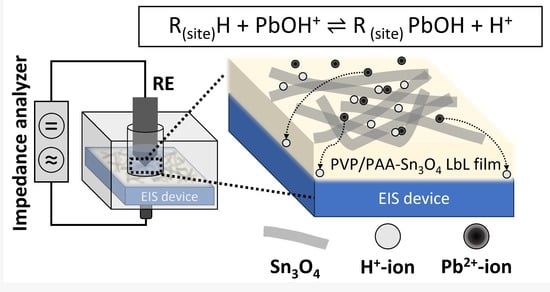
3. Results and Discussion

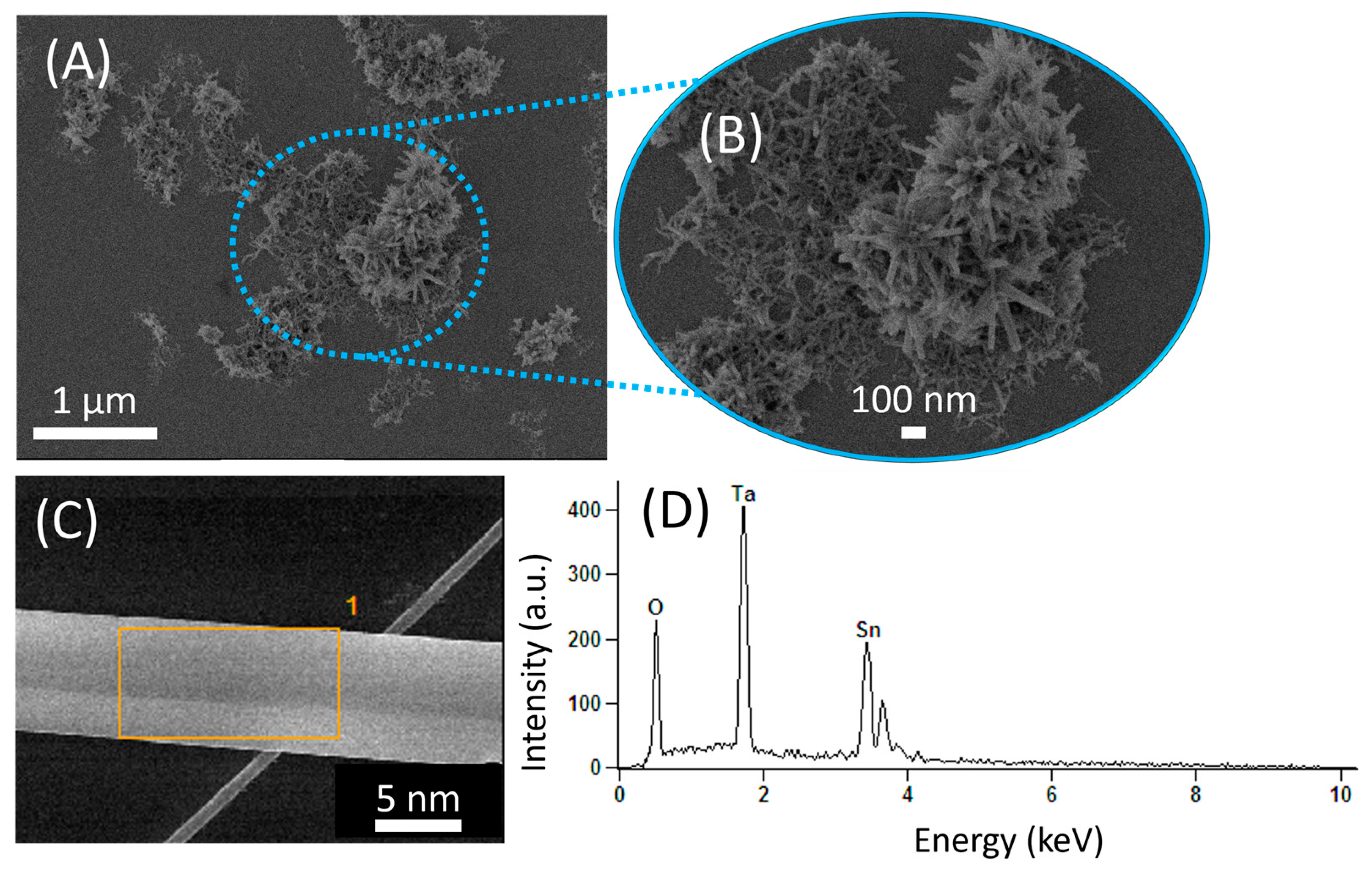
3.1. Surface Characterization of the LbL Film

Figure 2A,B show the FE-SEM images of a five-bilayer LbL film containing the Sn3O4 nanobelts on the EIS sensor chip. The microscopy and energy-dispersive X-ray spectroscopy (EDS) analyses revealed clusters of nanostructured Sn3O4 (from 100 nm to 400 nm) randomly arranged on the film, as seen in the enlarged dashed blue circle (Figure 2A,B). The formation of these clusters could be related to (I) the reduction in the size of the nanobelts, which may result from the ultrasonic power combined with the time required to obtain a stable dispersion of Sn3O4 in PAA solution; (II) the fact that Sn3O4 presents a high agglomeration tendency of one-dimensional (1D) nanostructures resulting from physical and chemical interactions, including van der Waals forces; (III) the possibility that during the formation of the layers through electrostatic interactions between PAA and PVP polymers, packaging of Sn3O4 nanomaterials may have occurred, which may be related to (II). Considering the agglomerated nanostructures observed, the prepared LbL film tends to exhibit a higher roughness and surface area, favoring the interaction of metallic ions with the nanobelt’s surface. Figure 2C presents the FE-SEM image of Sn3O4 nanostructures on LbL film after the deposition of five bilayers on the EIS chip. The elemental chemical analysis performed on the EIS chip (orange-marked region in Figure 2C) by EDS confirms the presence of Sn and O, along with Ta from the chip (Ta2O5), indicating the absence of contaminants in the prepared sensor chip.

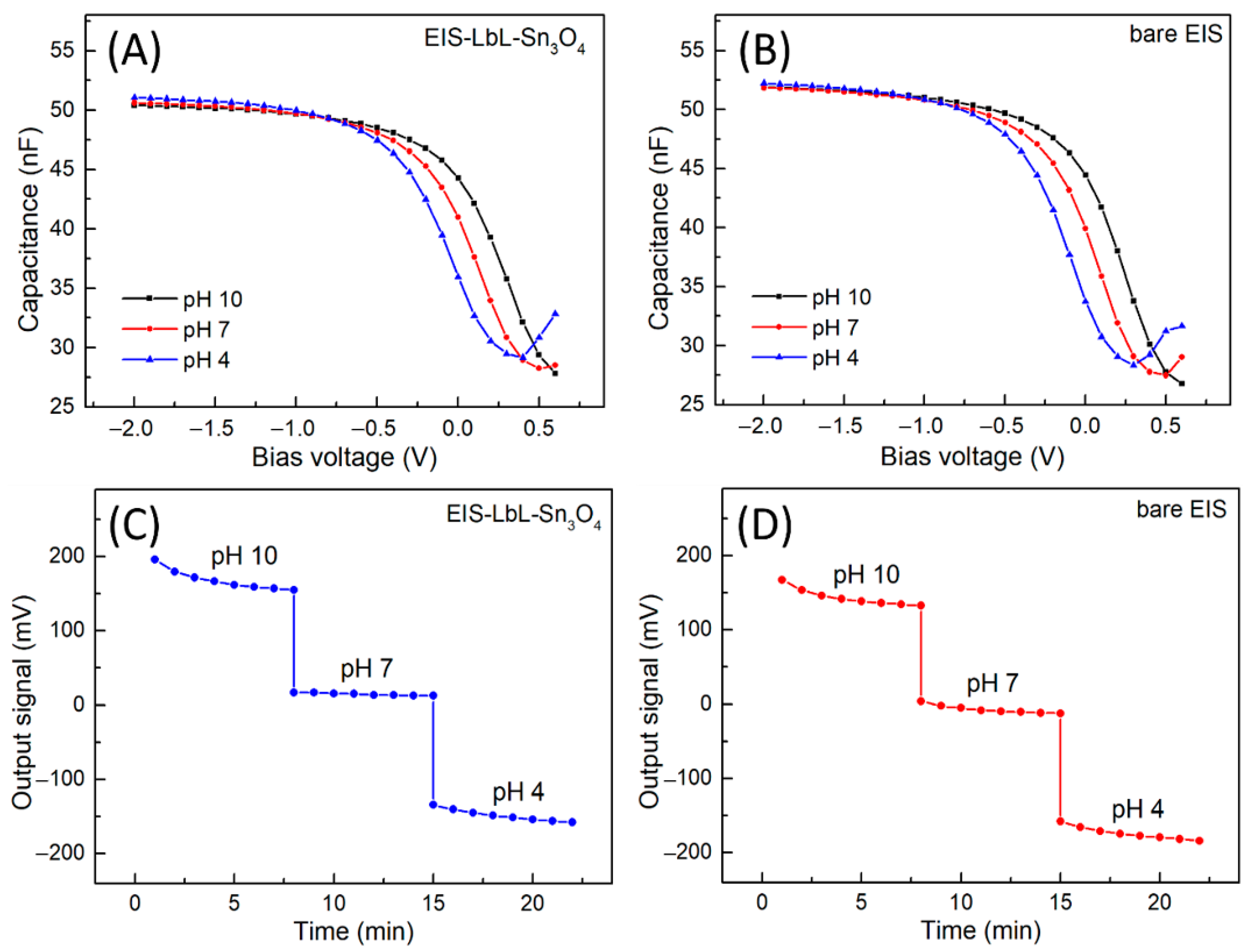
3.2. Electrochemical Characterization of the LbL Film

Figure 3 shows the C–V and ConCap curves for a five-bilayer EIS-Sn3O4 and a bare EIS sensor measured in a pH range of 4 to 10. The C–V curves (Figure 3A,B), occurring within a potential window of −2.0 V to 0.6 V (vs. Ag/AgCl), present a shift in the depletion region of both sensors (around −0.5 V to 0.5 V). The shift in this flat band region occurred for increasing positive potentials according to the pH increase due to concentration changes of the H+ ions that interact with the Ta2O5 sensor surface.
The dynamic temporal sensor response obtained from the ConCap curves is depicted in Figure 3C,D for EIS-Sn3O4 and bare EIS sensors, respectively. The measurements started from pH 10 to pH 4 in distinct potential levels, which tended toward stabilization during each concentration step. The EIS-Sn3O4 and bare EIS sensors exhibited comparable data from the ConCap curves in the pH range studied. At pH 10, the EIS-Sn3O4 sensor presented an average potential of ca. 150 mV. Then, the average potential changed to 0 mV and −150 mV as the pH decreased to 7 and 4, respectively. These results indicate that the modulation of the capacitance by the varying H+ ion concentration occurs according to the interaction between the ions and the Ta2O5 gate insulator surface (see also site binding theory [15,32]). The pH sensitivity was calculated for bare EIS and EIS-Sn3O4 sensors based on the averaged potentials measured for each pH value. Bare EIS resulted in a sensitivity of 52.9 mV/pH, while the EIS-Sn3O4 sensor reached 52.8 mV/pH. The achieved pH sensitivities are consistent with experimental data for Ta2O5 (55–58 mV/pH), as described in the literature [16,32,33].
In addition, the electrochemical characterization revealed that the sensitivity of the Ta2O5 surface toward H+ ions was not hampered by the growth of the LbL film with the PVP/PAA-Sn3O4 architecture on the field-effect sensor. The use of adequate concentrations of polymer and metal oxide for the film fabrication ensured that the surface of the sensor chip was not blocked by the interaction of H+ ions. This behavior was also noted in previous reports [13,16,17,18,34,35].

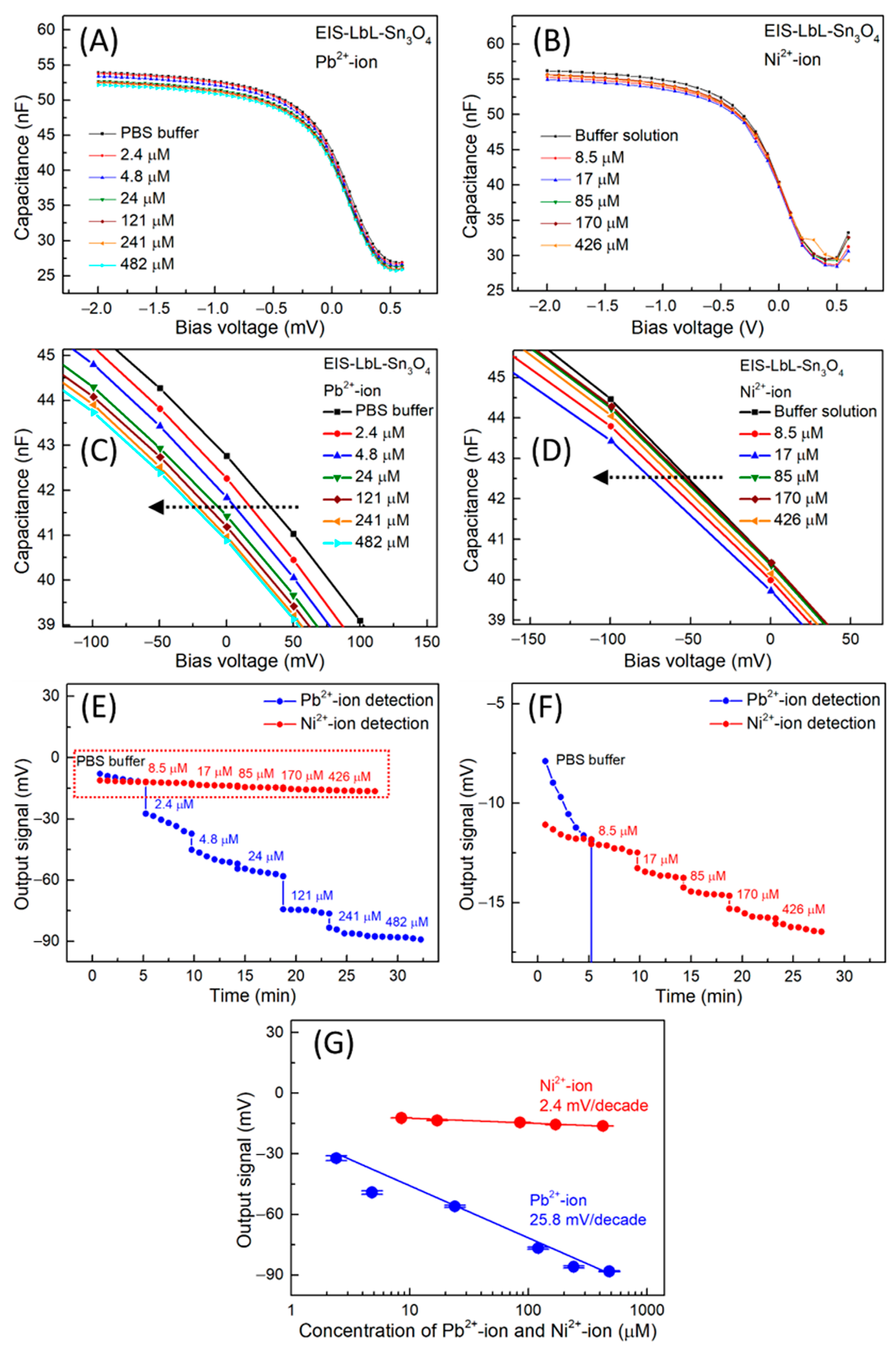
3.3. Detection of Pb2+ and Ni2+ Ions

Figure 4A,B present the C–V curves toward Pb2+ and Ni2+ ion detection using the EIS-Sn3O4 sensor. From these curves, one can note a variation of flat band capacitance in the depletion region with increasing analyte concentration when starting with buffer solution (PBS, pH 7). More precisely, a sequential variation for more negative potentials was verified from around −100 mV to around 100 mV in accordance with the increasing Pb2+ ion amount in the solution (Figure 4C, see also the direction of the arrow). It is important to note that this effect followed the same profile seen in the pH curves.
The interaction mechanism in the EIS-Sn3O4 sensor with Pb2+ ions can be attributed to the presence of the Sn3O4 nanobelts in the LbL film: In metal oxides, such as Fe3O4, SnO2, and TiO2, the interaction between the oxide surface and heavy metal ions occurs through an ion exchange reaction [36,37]. In an aqueous environment with pH 7, hydroxyl groups form available sites on the Sn3O4 surface. For solutions containing Pb2+ ions, the competition between H+ ions and Pb2+ ions results in an exchange of these ions in the sites releasing H+ ions in the solution [37]. The reaction that describes this interaction mechanism is expressed as follows:
RH + PbOH +     RPbOH + H +
where R represents the surface sites. In this way, the released H+ ions interact on the EIS surface, modulating the potential in the flat band region according to the increase in the Pb2+ ion concentration.
In contrast, only a small shift was observed, from −150 mV to 0.0 mV, in the C–V measurements for Ni2+ ion detection (Figure 4D). Here, based on surface reactions, the lower sensitivity exhibited by the EIS-Sn3O4 sensor may be associated with a weak exchange reaction between Ni2+ and H+ ions from the active sites on the film surface. This behavior could be related to the lower electronegativity of nickel than lead cations [38].
The ConCap curves obtained for different Pb2+ and Ni2+ ion concentrations are compared in Figure 4E. Starting with nearly equal potentials of bare EIS and EIS-Sn3O4 sensors for PBS buffer solution, the potential decreased for more negative values by increasing the respective ion concentration. Well-distinct plateaus were achieved for different concentrations of Pb2+ and Ni2+ ions (Figure 4E,F; here, “F” represents an enlarged view of “E” to illustrate the Ni2+ ion sensitivity). The calibration plots obtained from the ConCap curves are overviewed in Figure 4G: the EIS-Sn3O4 sensor exhibited an average sensitivity of 25.8 ± 0.5 mV/decade (R2 = 0.99) toward Pb2+ ions, and 2.4 ± 0.1 mV/decade (R2 = 0.99) for Ni2+ ions, which is a 10-fold difference.
These results clearly indicate the positive effect on the EIS sensitivity induced by the Sn3O4 LbL film with a higher affinity for Pb2+ ions. The limit of detection (LOD) toward Pb2+ ions was calculated using the equation (3xSD)/θ, where SD corresponds to the standard deviation of 10 C–V curves in buffer solution obtained from the flat band voltage for each sensor, and θ is the sensitivity calculated from the slope of the calibration curve. The LOD was estimated to be about 0.17 μM (34 μg/L) for the EIS-Sn3O4 sensor. Considering its practical application for lead detection, the EIS-Sn3O4 sensor presented a LOD close to the concentration limit recommended by the EPA (15 µg/L) and WHO (10 µg/L), and was also comparable with sensors using CuNPs/RGO [39], Fe3O4 [40], and MnFe2O4 [41], reported in the literature on Pb2+ ion detection.
As a control, the same procedure to detect Pb2+ and Ni2+ ions was also employed for a bare EIS sensor. As expected, the EIS-based Ta2O5 insulator gate did not exhibit strong cross-sensitivity towards these heavy metal ions. The LOD toward Pb2+ ions for the bare EIS sensor was estimated at ca. 1.2 μM (240 μg/L), which is seven times higher compared to the EIS-Sn3O4 sensor. This result demonstrates that the modification of the EIS sensor with Sn3O4 nanobelts in the form of LbL films was favorable to create a receptor sensing layer with improved sensitivity to detect heavy metals.
In this way, based on subsidiary reports [17,18,34], it can be inferred that the improved performance for heavy metal detection exhibited by the five-bilayer EIS-Sn3O4 sensor may be attributed to the ideal combination in terms of film architecture and amount of materials between PAA-Sn3O4 and PVP layers. The previous concentration analyzed to prepare a stable dispersion of nanobelts, and their subsequent distribution over the chip surface, permitted an adequate density/area coverage of the PAA-Sn3O4/PVP LbL film. The latter leads to an ideal condition of minimal resistance to ion transport between the exchange competition between H+ ions and Pb2+ ions, resulting in an enhanced EIS sensor.
Therefore, it is relevant to note the novel subjects and perspectives for environmental sensing introduced by the studied system, which is a proof of concept. Sensitive layers, based on LbL films of metal oxides, incorporated into an EIS device has been demonstrated to be advantageous, forming a viable and practical sensing platform. Furthermore, knowing the robustness and long lifetime of a device composed of an LbL film fabricated on an EIS sensing platform, the same EIS-Sn3O4 device may serve as sensing platform to be applied to further experiments for the detection of other heavy metal ions (e.g., Cd2+, Cu2+, and Hg2+) [13,16,17,18,35].

4. Conclusions

In conclusion, LbL films containing Sn3O4 nanobelts and polyelectrolytes were used to modify an EIS sensor chip as sensitive layers, and were tested to detect Pb2+ and Ni2+ ions. The successful immobilization of Sn3O4 nanobelts on the EIS sensor surface was confirmed by FE-SEM images. Electrochemical characterizations revealed that the sensitivity of the Ta2O5 gate insulator surface of the capacitive field-effect sensor was not impaired by the LbL film. The nanobelt-assisted sensor enabled the detection of Pb2+ and Ni2+ ions, conducted at pH 7. The electrochemical measurements showed a Pb2+ ion sensitivity of 25.1 mV/decade with a LOD of 0.17 μM (34 μg/L), which is comparable with other sensors reported in the literature. In contrast, the EIS-Sn3O4 sensor presented a lower sensitivity to the Ni2+ ion, which implies selectivity towards the Pb2+ ion. Moreover, EDS analysis proved that Pb2+ and Ni2+ ions are not adsorbed on surface of the LbL film after the electrochemical measurements, permitting the sensor to be reusable.
Future experiments will deal with long-term studies of the sensors, as well as the enlargement of the EIS-Sn3O4 sensor, to detect other interesting heavy metals, such as mercury, cadmium, and copper. Furthermore, this study has expanded the range of applications of Sn3O4 nanomaterials, which may help pave the way for their use in combination with other nanomaterials, such as carbon nanotubes and graphene, to develop sensors with improved properties for environmental monitoring.

Author Contributions

Conceptualization, P.V.M. and J.R.S.J.; methodology, P.V.M. and P.H.S.; formal analysis, P.V.M. and P.H.S.; investigation, P.V.M. and P.H.S.; resources, M.J.S., J.R.S.J. and M.O.O.; data curation, J.R.S.J., M.J.S. and M.O.O.; writing—original draft preparation, P.V.M. and P.H.S.; writing—review and editing, J.R.S.J., M.J.S. and M.O.O.; supervision, J.R.S.J. and M.O.O.; funding acquisition, M.O.O. All authors have read and agreed to the published version of the manuscript.

Funding

CAPES (Grant 88882.330127/2019-01), FAPEMIG (Grant APQ-01464-18), FAPESP (Grants 2017/26219-0 and 2016/20808-0), and CNPq (Grants 437785/2018-1, 426490/2018-5, and 152155/2022-8).

Institutional Review Board Statement

Not applicable.

Informed Consent Statement

Not applicable.

Data Availability Statement

Not applicable.

Acknowledgments

The authors acknowledge CAPES, FAPEMIG, FAPESP and CNPq for their financial support. The authors are grateful to the Rede Mineira de Química Network (Brazil), and to H. Iken for fabricating the Al/Si/SiO2/Ta2O5 sensor chips. TEM and FE-SEM facilities were provided by the IQ-UNESP.

Conflicts of Interest

The authors declare no conflict of interest.

References

  1. Ghosh, S.; Dissanayake, K.; Asokan, S.; Sun, T.; Rahman, B.M.A.; Grattan, K.T.V. Lead (Pb2+) Ion Sensor Development Using Optical Fiber Gratings and Nanocomposite Materials. Sens. Actuators B Chem. 2022, 364, 131818. [Google Scholar] [CrossRef]
  2. Jaishankar, M.; Tseten, T.; Anbalagan, N.; Mathew, B.B.; Beeregowda, K.N. Toxicity, Mechanism and Health Effects of Some Heavy Metals. Interdiscip. Toxicol. 2014, 7, 60–72. [Google Scholar] [CrossRef] [Green Version]
  3. Gumpu, M.B.; Sethuraman, S.; Krishnan, U.M.; Rayappan, J.B.B. A Review on Detection of Heavy Metal Ions in Water—An Electrochemical Approach. Sens. Actuators B Chem. 2015, 213, 515–533. [Google Scholar] [CrossRef]
  4. Cui, L.; Wu, J.; Ju, H. Electrochemical Sensing of Heavy Metal Ions with Inorganic, Organic and Bio-Materials. Biosens. Bioelectron. 2015, 63, 276–286. [Google Scholar] [CrossRef]
  5. Sang, S.; Zhang, H.; Sun, Y.; Jian, A.; Zhang, W. Facile Synthesis of Carbon-Encapsulated Fe3O4 Core/Shell Nanospheres for Application in Pb(II) Electrochemical Determination. Int. J. Electrochem. Sci. 2017, 12, 1306–1317. [Google Scholar] [CrossRef]
  6. EPA Basic Information about Lead in Drinking Water. Available online: https://www.epa.gov/ground-water-and-drinking-water/basic-information-about-lead-drinking-water#regs (accessed on 9 November 2022).
  7. World Health Organization. Biological Monitoring of Metals; World Health Organization: Geneva, Switzerland, 1994. [Google Scholar]
  8. Ezeonuegbu, B.A.; Machido, D.A.; Whong, C.M.Z.; Japhet, W.S.; Alexiou, A.; Elazab, S.T.; Qusty, N.; Yaro, C.A.; Batiha, G.E.-S. Agricultural Waste of Sugarcane Bagasse as Efficient Adsorbent for Lead and Nickel Removal from Untreated Wastewater: Biosorption, Equilibrium Isotherms, Kinetics and Desorption Studies. Biotechnol. Rep. 2021, 30, e00614. [Google Scholar] [CrossRef]
  9. Padilla, V.; Serrano, N.; Díaz-Cruz, J.M. Determination of Trace Levels of Nickel(II) by Adsorptive Stripping Voltammetry Using a Disposable and Low-Cost Carbon Screen-Printed Electrode. Chemosensors 2021, 9, 94. [Google Scholar] [CrossRef]
  10. EPA National Primary Drinking Water Regulations: Nickel. Available online: https://nepis.epa.gov/Exe/ZyNET.exe/9100PO2K.TXT?ZyActionD=ZyDocument&Client=EPA&Index=1995+Thru+1999&Docs=&Query=&Time=&EndTime=&SearchMethod=1&TocRestrict=n&Toc=&TocEntry=&QField=&QFieldYear=&QFieldMonth=&QFieldDay=&IntQFieldOp=0&ExtQFieldOp=0&XmlQuery= (accessed on 9 November 2022).
  11. World Health Organization. Nickel in Drinking-Water; World Health Organization: Geneva, Switzerland, 2021. [Google Scholar]
  12. Poghossian, A.; Schöning, M.J. Capacitive Field-Effect EIS Chemical Sensors and Biosensors: A Status Report. Sensors 2020, 20, 5639. [Google Scholar] [CrossRef]
  13. Oliveira, D.A.; Gasparotto, L.H.S.; Siqueira, J.R., Jr. Processing of Nanomaterials in Layer-by-Layer Films: Potential Applications in (Bio)Sensing and Energy Storage. An. Acad. Bras. Ciências 2019, 91, 1–17. [Google Scholar] [CrossRef]
  14. Poghossian, A.; Schöning, M.J. Recent Progress in Silicon-Based Biologically Sensitive Field-Effect Devices. Curr. Opin. Electrochem. 2021, 29, 100811. [Google Scholar] [CrossRef]
  15. Oliveira, O.N.; Iost, R.M.; Siqueira, J.R., Jr.; Crespilho, F.N.; Caseli, L. Nanomaterials for Diagnosis: Challenges and Applications in Smart Devices Based on Molecular Recognition. ACS Appl. Mater. Interfaces 2014, 6, 14745–14766. [Google Scholar] [CrossRef]
  16. Morais, P.V.; Gomes, V.F.; Silva, A.C.A.; Dantas, N.O.; Schöning, M.J.; Siqueira, J.R., Jr. Nanofilm of ZnO Nanocrystals/Carbon Nanotubes as Biocompatible Layer for Enzymatic Biosensors in Capacitive Field-Effect Devices. J. Mater. Sci. 2017, 52, 12314–12325. [Google Scholar] [CrossRef]
  17. Morais, P.V.; Orlandi, M.O.; Schöning, M.J.; Siqueira, J.R., Jr. Layer-by-Layer Films with CoFe2O4 Nanocrystals and Graphene Oxide as a Sensitive Interface in Capacitive Field-Effect Devices. ACS Appl. Nano Mater. 2022, 5, 5258–5267. [Google Scholar] [CrossRef]
  18. Morais, P.V.; Silva, A.C.A.; Dantas, N.O.; Schöning, M.J.; Siqueira, J.R., Jr. Hybrid Layer-by-Layer Film of Polyelectrolytes-Embedded Catalytic CoFe2O4 Nanocrystals as Sensing Units in Capacitive Electrolyte-Insulator-Semiconductor Devices. Phys. Status Solidi 2019, 216, 1900044. [Google Scholar] [CrossRef]
  19. Suman, P.H.; Felix, A.A.; Tuller, H.L.; Varela, J.A.; Orlandi, M.O. Comparative Gas Sensor Response of SnO2, SnO and Sn3O4 Nanobelts to NO2 and Potential Interferents. Sens. Actuators B Chem. 2015, 208, 122–127. [Google Scholar] [CrossRef]
  20. Li, L.; Zhang, C.; Chen, W. Fabrication of SnO2–SnO Nanocomposites with p–n Heterojunctions for the Low-Temperature Sensing of NO2 Gas. Nanoscale 2015, 7, 12133–12142. [Google Scholar] [CrossRef] [PubMed]
  21. Li, Y.-X.; Guo, Z.; Su, Y.; Jin, X.-B.; Tang, X.-H.; Huang, J.-R.; Huang, X.-J.; Li, M.-Q.; Liu, J.-H. Hierarchical Morphology-Dependent Gas-Sensing Performances of Three-Dimensional SnO2 Nanostructures. ACS Sens. 2017, 2, 102–110. [Google Scholar] [CrossRef]
  22. Chen, H.; Yang, X.; Feng, W. Cadmium-Ion Detection: A Comparative Study for a SnO2, MoS2, SnO2/MoS2, SnO2-MoS2 Sensing Membrane Combination with a Fiber-Optic Mach–Zehnder Interferometer. Appl. Opt. 2021, 60, 799–804. [Google Scholar] [CrossRef]
  23. Gu, R.; Zhao, Y.; Fu, H.; Yang, J.; Hu, Z.; Li, L.; Li, H.-Y.; Huang, Q.; Chen, B.; Liu, H. Nanocrystalline SnO2-Modified Electrode for Ultra-Sensitive Mercury Ion Detection. IEEE Sens. J. 2022, 22, 7590–7598. [Google Scholar] [CrossRef]
  24. Kaur, H.; Bhatti, H.S.; Singh, K. Pr Doped SnO2 Nanostructures: Morphology Evolution, Efficient Photocatalysts and Fluorescent Sensors for the Detection of Cd2+ Ions in Water. J. Photochem. Photobiol. A Chem. 2020, 388, 112144. [Google Scholar] [CrossRef]
  25. Suman, P.H.; Longo, E.; Varela, J.A.; Orlandi, M.O. Controlled Synthesis of Layered Sn3O4 Nanobelts by Carbothermal Reduction Method and Their Gas Sensor Properties. J. Nanosci. Nanotechnol. 2014, 14, 6662–6668. [Google Scholar] [CrossRef] [PubMed]
  26. Chen, D.; Yu, W.; Wei, L.; Ni, J.; Li, H.; Chen, Y.; Tian, Y.; Yan, S.; Mei, L.; Jiao, J. High Sensitive Room Temperature NO2 Gas Sensor Based on the Avalanche Breakdown Induced by Schottky Junction in TiO2-Sn3O4 Nanoheterojunctions. J. Alloys Compd. 2022, 912, 165079. [Google Scholar] [CrossRef]
  27. He, Y.; Li, D.; Chen, J.; Shao, Y.; Xian, J.; Zheng, X.; Wang, P. Sn3O4: A Novel Heterovalent-Tin Photocatalyst with Hierarchical 3D Nanostructures under Visible Light. RSC Adv. 2014, 4, 1266–1269. [Google Scholar] [CrossRef]
  28. Yang, R.; Song, G.; Wang, L.; Yang, Z.; Zhang, J.; Zhang, X.; Wang, S.; Ding, L.; Ren, N.; Wang, A.; et al. Full Solar-Spectrum-Driven Antibacterial Therapy over Hierarchical Sn3O4/PDINH with Enhanced Photocatalytic Activity. Small 2021, 17, 2102744. [Google Scholar] [CrossRef]
  29. Jose Damaschio, C.; Berengue, O.M.; Stroppa, D.G.; Simon, R.A.; Ramirez, A.J.; Herwig Schreiner, W.; Chiquito, A.J.; Leite, E.R. Sn3O4 Single Crystal Nanobelts Grown by Carbothermal Reduction Process. J. Cryst. Growth 2010, 312, 2881–2886. [Google Scholar] [CrossRef]
  30. Orlandi, M.O.; Suman, P.H.; Silva, R.A.; Arlindo, E.P.S. Carbothermal Reduction Synthesis: An Alternative Approach to Obtain Single-Crystalline Metal Oxide Nanostructures BT. In Recent Advances in Complex Functional Materials: From Design to Application; Longo, E., La Porta, F.A., Eds.; Springer International Publishing: Cham, Switzerland, 2017; pp. 43–67. ISBN 978-3-319-53898-3. [Google Scholar]
  31. Schöning, M.J.; Brinkmann, D.; Rolka, D.; Demuth, C.; Poghossian, A. CIP (Cleaning-in-Place) Suitable “Non-Glass” PH Sensor Based on a Ta2O5-Gate EIS Structure. Sens. Actuators B Chem. 2005, 111–112, 423–429. [Google Scholar] [CrossRef]
  32. Schöning, M.J.; Poghossian, A. Bio FEDs (Field-Effect Devices): State-of-the-Art and New Directions. Electroanalysis 2006, 18, 1893–1900. [Google Scholar] [CrossRef]
  33. Schöning, M.J. “Playing around” with Field-Effect Sensors on the Basis of EIS Structures, LAPS and ISFETs. Sensors 2005, 5, 126–138. [Google Scholar] [CrossRef] [Green Version]
  34. Sousa, M.A.M.; Siqueira, J.R., Jr.; Vercik, A.; Schöning, M.J.; Oliveira, O.N. Determining the Optimized Layer-by-Layer Film Architecture with Dendrimer/Carbon Nanotubes for Field-Effect Sensors. IEEE Sens. J. 2017, 17, 1735–1740. [Google Scholar] [CrossRef]
  35. Siqueira, J.R., Jr.; Molinnus, D.; Beging, S.; Schöning, M.J. Incorporating a Hybrid Urease-Carbon Nanotubes Sensitive Nanofilm on Capacitive Field-Effect Sensors for Urea Detection. Anal. Chem. 2014, 86, 5370–5375. [Google Scholar] [CrossRef]
  36. Rehman, M.; Rehman, W.; Waseem, M.; Hussain, S.; Haq, S.; Rehman, M.A. Adsorption Mechanism of Pb2+ Ions by Fe3O4, SnO2, and TiO2 Nanoparticles. Environ. Sci. Pollut. Res. 2019, 26, 19968–19981. [Google Scholar] [CrossRef] [PubMed]
  37. Moradi, A.; Najafi Moghadam, P.; Hasanzadeh, R.; Sillanpää, M. Chelating Magnetic Nanocomposite for the Rapid Removal of Pb(Ii) Ions from Aqueous Solutions: Characterization, Kinetic, Isotherm and Thermodynamic Studies. RSC Adv. 2017, 7, 433–448. [Google Scholar] [CrossRef] [Green Version]
  38. Fialova, D.; Kremplova, M.; Melichar, L.; Kopel, P.; Hynek, D.; Adam, V.; Kizek, R. Interaction of Heavy Metal Ions with Carbon and Iron Based Particles. Materials 2014, 7, 2242–2256. [Google Scholar] [CrossRef]
  39. Li, D.; Wang, C.; Zhang, H.; Sun, Y.; Duan, Q.; Ji, J.; Zhang, W.; Sang, S. A Highly Effective Copper Nanoparticle Coupled with RGO for Electrochemical Detection of Heavy Metal Ions. Int. J. Electrochem. Sci. 2017, 12, 10933–10945. [Google Scholar] [CrossRef]
  40. Fan, H.-L.; Zhou, S.-F.; Gao, J.; Liu, Y.-Z. Continuous Preparation of Fe3O4 Nanoparticles through Impinging Stream-Rotating Packed Bed Reactor and Their Electrochemistry Detection toward Heavy Metal Ions. J. Alloys Compd. 2016, 671, 354–359. [Google Scholar] [CrossRef]
  41. Han, X.-J.; Zhou, S.-F.; Fan, H.-L.; Zhang, Q.-X.; Liu, Y.-Q. Mesoporous MnFe2O4 Nanocrystal Clusters for Electrochemistry Detection of Lead by Stripping Voltammetry. J. Electroanal. Chem. 2015, 755, 203–209. [Google Scholar] [CrossRef]
Figure 1. (A) Scheme of the bare EIS device with p-Si-SiO2-Ta2O5 structure. (B) Representation of one bilayer for a PVP/PAA-Sn3O4 LbL film fabricated on the EIS surface. (C) Scheme showing the experimental apparatus for electrochemical measurements using the EIS-Sn3O4 sensor.
Chemosensors 11 00436 g001
Figure 2. (A) FE-SEM image of a five-bilayer LbL film containing Sn3O4 nanobelts on the EIS chip, and (B) its enlarged image of nanobelt agglomeration. (C) FE-SEM image of Sn3O4 showing the region analyzed by EDS, followed by (D) the elemental EDS spectrum.
Chemosensors 11 00436 g002
Figure 3. (A,B) C–V and (C,D) ConCap curves for pH detection ranging from 4 to 10 for the EIS-LbL-Sn3O4 and bare EIS sensors.
Chemosensors 11 00436 g003
Figure 4. Example C–V curves of an EIS-Sn3O4 sensor for (A) Pb2+ and (B) Ni2+ ion detection. Enlarged depletion regions from C–V curves for (C) Pb2+ and (D) Ni2+ ion detection. ConCap recording for Pb2+ and Ni2+ ion detection (E) and enlarged view (F) for Ni2+, as well as resulting calibration curves (G).
Chemosensors 11 00436 g004
Disclaimer/Publisher’s Note: The statements, opinions and data contained in all publications are solely those of the individual author(s) and contributor(s) and not of MDPI and/or the editor(s). MDPI and/or the editor(s) disclaim responsibility for any injury to people or property resulting from any ideas, methods, instructions or products referred to in the content.

