Article

Three Generations of Surface Nanocomposites Based on Hexagonally Ordered Gold Nanoparticle Layers and Their Application for Surface-Enhanced Raman Spectroscopy

by
Shireen Zangana
1,2,
Tomáš Lednický
3 and
Attila Bonyár
1,2,*
1
Department of Electronics Technology, Faculty of Electrical Engineering and Informatics, Budapest University of Technology and Economics, 1111 Budapest, Hungary
2
Wigner Research Centre for Physics, 1525 Budapest, Hungary
3
CEITEC—Central European Institute of Technology, Brno University of Technology, 61200 Brno, Czech Republic
*
Author to whom correspondence should be addressed.
Chemosensors 2023, 11(4), 235; https://doi.org/10.3390/chemosensors11040235
Submission received: 28 February 2023 / Revised: 5 April 2023 / Accepted: 6 April 2023 / Published: 10 April 2023
(This article belongs to the Special Issue Nanocomposites for SERS Sensing)

Abstract

:
The fabrication technology of surface nanocomposites based on hexagonally ordered gold nanoparticle (AuNP) layers (quasi-arrays) and their possible application as surface-enhanced Raman spectroscopy (SERS) substrates are presented in this paper. The nanoparticle layers are prepared using a nanotextured template formed by porous anodic alumina (PAA) and combined with gold thin-film deposition and subsequent solid-state dewetting. Three types of hexagonal arrangements were prepared with different D/D0 values (where D is the interparticle gap, and D0 is the diameter of the ellipsoidal particles) on a large surface area (~cm2 range), namely, 0.65 ± 0.12, 0.33 ± 0.10 and 0.21 ± 0.09. The transfer of the particle arrangements to transparent substrates was optimized through three generations, and the advantages and disadvantages of each transfer technology are discussed in detail. Such densely packed nanoparticle arrangements with high hot-spot density and tunable interparticle gaps are very beneficial for SERS applications, as demonstrated with two practical examples. The substrate-based enhancement factor of the nanocomposites was determined experimentally using a DNA monolayer and was found to be between 4 × 10⁴ and 2 × 10⁶ for the different particle arrangements. We also determined the sensing characteristics of a small dye molecule, rhodamine 6G (R6G). By optimizing the experimental conditions (e.g., optimizing the laser power and the refractive index of the measurement medium with an ethylene-glycol/water mixture), concentrations as low as 10−16 M could be detected at 633 nm excitation.

1. Introduction

Surface-enhanced Raman spectroscopy (SERS) is a powerful analytical technique widely used in the fields of chemistry [1], biology [2], materials science [3], point-of-care and clinical diagnostics [4,5], environmental monitoring [6,7] and food quality and safety [8]. This surface-sensitive technique provides high sensitivity and selectivity for detecting molecules adsorbed onto metallic surfaces. The Fleischmann group, who first observed SERS on a roughened silver electrode [9], reported a Raman scattering enhancement by a factor of 105–106. Since this observation, researchers’ interest has rapidly grown to develop and improve this technique. The enhancement of Raman signals in SERS can now result in enormous amplifications (up to 1010–1011 [10]), leading to even single-molecule detection limits [11], which has opened new opportunities for detecting and analyzing trace amounts of molecules, expanding its possible applications even wider [12].
Electromagnetic enhancement is the primary mechanism for enhancing the Raman signal in SERS [13]. It results from the interaction between the incident electromagnetic field and the localized surface plasmon resonances (LSPRs) of metallic nanostructures. The electromagnetic field of the incident light induces an oscillation of the electrons in the metal, generating a highly localized and enhanced electromagnetic field at the surface of the nanostructure. This enhanced field, in turn, enhances the Raman signal of the adsorbed molecule by several orders of magnitude.
On the other hand, the chemical enhancement mechanism arises from the charge transfer or resonance effects between the adsorbed molecule and the metallic nanostructure. This mechanism can enhance the Raman signal of some specific molecules, such as those containing unsaturated bonds or functional groups, and can contribute to the overall enhancement observed in SERS [14,15].
Understanding the mechanisms of Raman scattering enhancement in SERS is crucial for designing and optimizing SERS substrates for various applications. Factors such as the morphology, size, and composition of the metallic nanostructures and the distance between the molecule and the surface can all significantly influence the yield of Raman scattering in SERS by affecting the two main enhancement mechanisms. Considering the electromagnetic enhancement, maximizing the hot-spot density of the utilized nanostructures is of utmost importance.
In recent years, we have developed a technology to control and maximize the hot-spot density on large surface areas by using hexagonally ordered AuNP layers prepared on porous anodic alumina templates [16]. The main advantage of this technology is the uniformly controlled particle size and interparticle gap on a large (cm2) surface area with which the plasmonic coupling between the particles and their plasmon absorbance spectrum can be influenced. The nanoparticle arrangement can be transferred to a transparent support material, such as PDMS (polydimethylsiloxane) or epoxy, forming a surface nanocomposite. With the second generation of these nanocomposites, successful applications, such as LSPR sensors or SERS substrates, have been reported for nucleic acid detection [16,17].
In the present paper, for the first time, a third generation of nanocomposites is reported that utilizes a thin SiO2 film as a transfer substrate, glued to a microscopic slide acting as a support material. With this technological advancement, the thermal stability of the substrates improves significantly, enabling the utilization of the substrates at excitation wavelengths close to the plasmon absorption peak of the nanostructures (e.g., 633 nm).
As well as presenting the fabrication technology in detail, two application areas of both the second and the third generation of nanocomposites is demonstrated. With the help of DNA monolayers, the substrate-specific enhancement factor (SSEF) is determined for nanoparticle arrangements with different densities, demonstrating the importance of interparticle gaps on the SERS enhancement. Secondly, using the third generation of nanocomposites, we demonstrate how the relationship between the laser excitation wavelength and the plasmon absorbance peak of the substrate influences the obtainable Raman signals, and, by optimizing these parameters, we demonstrate an ultralow molecular limit of detection (LOD) for rhodamine 6G.

2. Materials and Methods
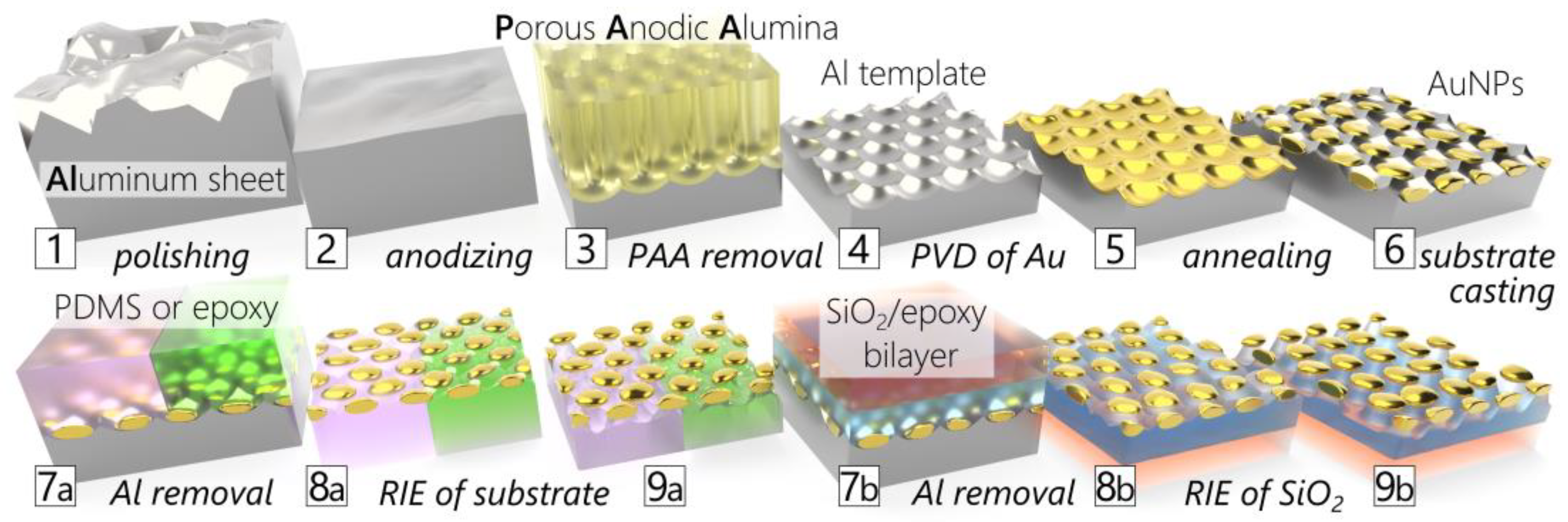
2.1. Fabrication

The fabrication technology of three generations of gold nanoparticle (AuNP) composites is illustrated in Figure 1. The fabrication of the aluminum template and the synthesis of AuNP layers (Figure 1: 1–6) are the same for all generations. These steps are described in detail in our previous works [16,17], including the optimization of the process parameters and additional distributions of AuNPs. In summary, a 250 μm thick high-purity (99.999%) aluminum sheet (Goodfellow Cambridge Ltd., Huntingdon, UK) was cleaned, vacuum-annealed (550 °C, 15 h), and mechanically and electrochemically polished (Figure 1: 1–2). Then, the sheet was anodized (40 V, 0.3 M oxalic acid, 8 °C, 20 h) to form well-ordered porous anodic alumina (PAA) that was selectively etched, resulting in a nanobowled Al template (Figure 1: 2–4). AuNPs were synthesized by a template-assisted solid-state dewetting of the magnetron-sputtered Au film (Figure 1: 4–6). The size of AuNPs can be increased by repeating this process. The three AuNP distributions created using subsequent annealing of 8 nm + 7 nm + 5.5 nm thick Au films is presented and discussed in Section 3.1. Afterward, the synthesized AuNP arrangements were transferred to a transparent and dielectric substrate to utilize their optical properties (Figure 1: 7–9). Before transfer, AuNPs were O2:Ar (80:20) plasma-cleaned for 5 min at 300 W and 50 Pa.
This work presents three technological generations using different substrates: bulk-casted polydimethylsiloxane (PDMS), epoxy, and a thin film of SiO2. The first (PDMS) and second (epoxy) generations use a bulk substrate as support (Figure 1: 7a–9a). For the first generation, the adhesion of AuNPs to PDMS needed to be promoted by a (3-mercaptopropyl)trimethoxysilane (MPTMS) layer. It was deposited by drop-casting over AuNPs (0.5 μlcm−2) in ethanol (99.8%, 20 mL) and left for 1 h with gentle stirring. Immediately before PDMS casting, it was washed with ethanol and dried with nitrogen. PDMS was prepared using a two-part elastomer kit (SYLGARD® 184, Dow Chemical, Midland, MI, USA) with a standard mixing ratio of 10:1, degassed, cast in a thickness of ~5 mm, and cured at 80 °C for min. 2 h. Similarly, in the second generation, a two-compound epoxy resin (Elan-tron EC 570 and W363, ratio 100:33) was cast directly on the AuNP surface and cured at 50 °C for 12 h. Both SYLGARD® 184 PDMS and Elan-tron EC 570 and W363 were purchased from ELCHEM Co., Zruč nad Sázavou, Czech Republic.
The third generation utilized thin SiO2 film as a substrate glued to a microscopic slide acting as a support. The SiO2 film (~300 nm) was partly deposited (~20 nm) by e-beam evaporation (0.05 nm/s, 10−4 Pa) to avoid cross-contamination of the PECVD chamber by Au. The rest of the thickness was deposited in PECVD (40 min, ICP = 600 W, 400 Pa, 3:13 sccm of SiH4:N2O, PlasmaPro 100, Oxford Instruments Plasma Technology, Yatton, UK). The PECVD process was chosen to avoid cracking of the film due to high stress, which is common for evaporated films. The resulting sandwich structure (Al/AuNPs/SiO2) was glued by a general-purpose two-compound epoxy (Loctite 3430) to a 1 mm thick microscopic glass slide (Figure 1: 7b).
Then, the Al template was selectively etched (Figure 1: 7–8, same for all generations) in an HCl (35% w/w) and CuCl2 (2 M) water solution. Before, the aluminum sheet was gently scratched to promote the etching speed, and a Kapton tape was applied to avoid corrosion of the support. After that, the sample was subsequently immersed in FeCl3 (2 M) and H3PO4 (10%, 40 °C) water solution for 5 min to remove copper and aluminum oxide residues.
Transferred AuNPs were still embedded in the substrate (Figure 1: 8), which would hinder their accessibility and, thus, the performance of the sensor. Therefore, the final step was the controlled removal of the substrate by reactive ion etching (RIE). For all generations, a PlasmaPro 80 (Oxford Instruments Plasma Technology, Yatton, United Kingdom) was used: PDMS (80 s, 50 W, 6.7 Pa, SF6:O2 5:1, 60 sccm), epoxy (40 s, 50 W, 6.7 Pa, O2, 50 sccm) [16], SiO2 precleaning (60 s, 100 W, 13.3 Pa, O2, 20 sccm), and SiO2 etching (120 s, 100 W, 4 Pa, Ar:CHF3:O2 6:3:1, 50 sccm). Lastly, samples were cut to appropriate sizes by a razor (PDMS), a circular saw (epoxy), and a dicing saw (SiO2), washed with isopropyl alcohol, and dried with nitrogen. The prepared nanocomposites are shown in Figure 2.

2.2. Substrate Characterization

The plasmon wavelength of the fabricated substrate was investigated using a Cary 400 UV-VIS spectrophotometer. Scanning electron microscopy (SEM) was performed with a high-resolution SEM (Verios 460 L, Thermo Fisher Scientific, Brno, Czech Republic) in the immersion, using secondary electron (SE) mode and an acceleration voltage of 5 keV. Scanning transmission electron microscopy (STEM) was performed with a dual-beam SEM/FIB system (Helios NanoLab 660, Thermo Fisher Scientific, Brno, Czech Republic) using a STEM detector in bright-field (BF) mode and an operating voltage of 23 keV. The evaluation of the AuNP size was performed by image processing software (Adobe Photoshop, Gwyddion) as presented in the Supplementary Materials data.

2.3. Sample Preparation for SERS Measurements

Before any SERS measurement, the first step was always the cleaning of the SERS substrates with O2 plasma at 20 W, 40 Pa for 15 s in a Diener Electronic (Ebhausen, Germany) Atto plasma surface treatment machine.
Rhodamine 6G, DNA oligomers and ethylene-glycol were purchased from Sigma Aldrich Ltd. (part of Merck KGaA, Darmstadt, Germany). For the experiments R6G of 1 × 10⁻⁴ M was added to a solution of ethylene glycol/water mixtures in different ratios (25%, 50%, 75%, and 100%).
For the DNA experiments a 20-bases-long sequence (CGTACATCTTCTTCCTTTTT(ThiC6)) was used to coat the surface of the gold nanoparticles with a DNA monolayer. The coating solution contained 1 μM DNA in a buffer consisting of 0.75 M NaCl and 50 μM Na2HPO4 (pH 6.8) in deionized water. Immobilization of DNA was performed overnight after drop-coating the SERS substrates and sealing them inside a humidified Petri dish. The same buffer was used to clean the substrates before the SERS experiments.

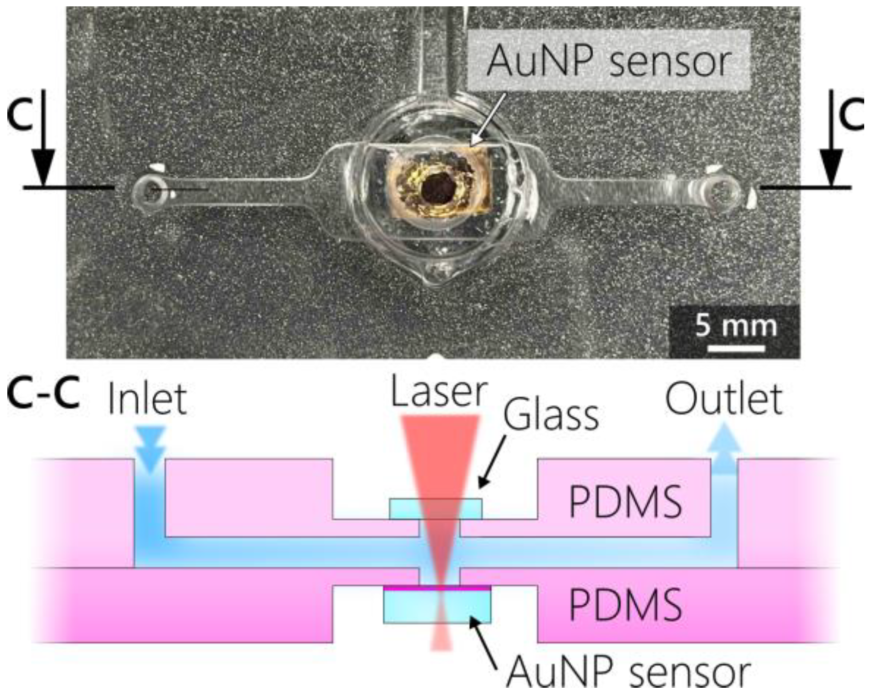
2.4. PDMS Microfluidic Cell Fabrication

For the experiments performed on the third generation of nanocomposites with the R6G solutions (Section 3.4), a PDMS microfluidic cell was prepared by mixing SYLGARD® 184 silicone elastomer with its corresponding curing agent in a 5:1 mass ratio. The mixture was degassed in a vacuum exicator and poured into custom-designed 3D-printed case molding forms. The molding forms were placed in a ceramic oven for 45 min at 80 °C to increase the polymerization speed. The design and the completed cell are presented in Figure 3. The cell consisted of two molded PDMS parts. The bottom part incorporated the nanocomposite sensor, while the upper part contained the microfluidic channel (with input and output ports). Directly atop the nanocomposite substrate, the cell was hermetically sealed with a calcium-fluoride glass that does not interfere with Raman spectroscopy. The two PDMS parts were bonded together after corona discharge treatment, as discussed in [18].

2.5. Raman Spectroscopy

A Renishaw inVia micro-Raman spectrometer with three different excitation laser wavelengths was used to perform the SERS measurements. The first source, with an excitation wavelength of 633 nm, was used for the R6G experiments. This source has a maximal laser output power of 10 mW and was used either with 1% (0.1 mW) or 5% (0.5 mW) power, as indicated in the results section. The second excitation wavelength of 785 nm was used for the DNA experiments with 100% output power (20 mW). In all cases, a 10 s exposure time and 5 accumulations were used for the measurements, including both SERS and normal Raman performed on the 10 mM reference DNA solution. The laser beam was focused with an objective of 50× magnification and a numerical aperture (NA) of 0.55 (type LWD50X). With this objective, the spot diameter of the laser beam was ~1.8 mm on the sample surface. For the SERS EF calculations, a z-dimensional scan mode was also used to map the peak intensities along the normal direction (perpendicular to the substrate surface), using a Renishaw MS30 high-speed encoded stage, an objective with 100× magnification (NA = 0.9) and a pinhole (~10 μm) with a confocal depth profiling step size of 100 nm. The spot diameter was ~0.9 mm with this objective. In Section 3.2, excitation with 532 nm source is mentioned, regarding the thermal stability of the substrate. This refers to experiments with 0.6 mW power and the same 50× objective with 0.55 NA.

3. Results and Discussion

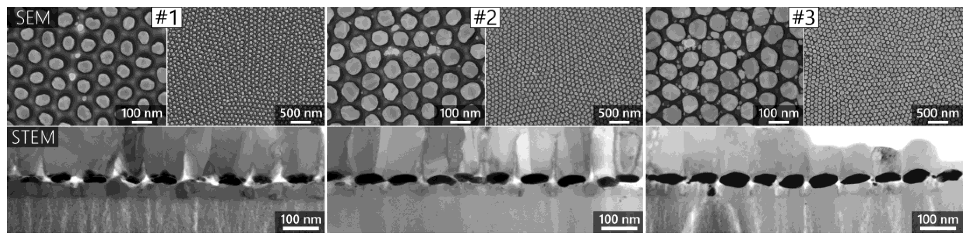
3.1. AuNP Layers Characterization

Figure 4 demonstrates well-ordered AuNPs in a few micron-size planar domains forming 2D hexagonal quasi-arrays. The distribution of AuNPs is inherited from the aluminum template with a cell size of (110.9 ± 7.3) nm and a cell density of (91 ± 1) μm−2.
Here, we demonstrate three AuNP arrangements of different sizes of AuNPs (calculated in Table 1), which were prepared by additional repetitions of Au thin film deposition and solid-state dewetting (SSD) processes (Figure 4: 4–6). Notably, with increased size of AuNPs, the density of defects also increased, such as through the merging of adjacent NPs and the occurrence of small satellite NPs (illustrated in the Supplementary Materials). The cause was the lower template contribution to control SSD, as well as a compromised conformality of the deposited thin film due to decreasing thickness and more complex surface morphology.
The possibility of hot-spot engineering to precisely control the particle size and interparticle gap of the arrangement on a large surface area is especially important for SERS applications. Although small gaps are usually desired for larger near-field intensities and higher enhancement factors, one also has to consider the size of the target molecules and make sure that the molecules can fit in the hot-spots for optimal sensing performance [19,20]. Thus, the ability to tune the interparticle gaps and, thus, tailor the hot-spots with respect to the different target molecules could be one of the most significant advantages of the proposed SERS substrate.

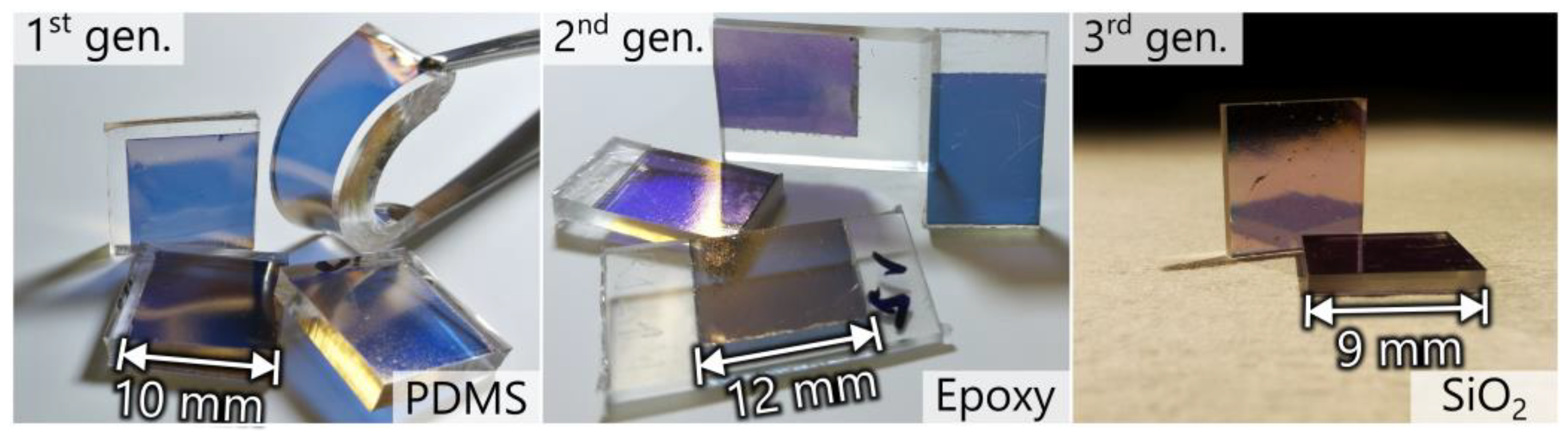
3.2. Three Generations of Nanocomposites

The first generation of nanocomposite, utilizing PDMS (Figure 2) as a gold standard, was focused on a straightforward integration of AuNP layers within a microfluidic chip, which was demonstrated in our previous work [21]. The main issue with this approach was sensitivity degradation to almost zero in ~2 weeks. In contrast to a similar effect caused by hydrocarbon contamination (reported for the second generation [16], and later observed also in the third generation), this degradation was mostly attributed to the migration of free species (oligomers) from the PDMS substrate toward AuNPs. This hypothesis was indirectly supported by an inability to recover the sensitivity by oxygen plasma cleaning (a standard procedure before, e.g., AuNP hybridization) that worked well for both second and third generations, but only fluorine plasma was able to recover the sensitivity of the first generation. In addition, the migration of free silicone species from PDMS was also reported for different applications [22,23]. In summary, the first generation demonstrated that, despite numerous desired properties of PDMS, it was a poor choice for surface-sensitive applications due to its high contamination rate and inconvenient cleaning procedure.
Therefore, in the second generation, PDMS was substituted by an epoxy resin (illustrated in Figure 1: 9a, photograph in Figure 2). The second generation circumvented the cleaning incapability along with increased sensitivity of AuNPs due to better RIE control and substrate stability. In our previous work [16], we demonstrated successful LSPR-based detection of DNA over such AuNP-epoxy nanocomposites. However, the properties of epoxy resin, such as chemical and thermal stability, are limiting for more demanding applications. The chemical stability needs to be considered to avoid dissolution or yellowing during the fabrication process. Good thermal stability is important during RIE as well as for SERS measurements, where high-power laser irradiation causes surface damage, especially for laser wavelengths (532 and 633 nm) close to the plasmon excitation. Lastly, the number of cleanings (reusability) is limited because the epoxy substrate is slightly etched during an oxygen plasma cycle.
The main success of the third generation was overcoming the oxygen plasma cleaning limitation and stability by utilizing a thin SiO2 substrate. The SiO2 film also improved the thermal stability while allowing SERS measurements using 532 nm or 633 nm laser sources. With the second generation substrates, even laser powers around 0.5 mW were shown to damage the epoxy substrate at these wavelengths (see Supplementary Materials). As is demonstrated in Section 3.4., the third generation substrates were stable at these powers. The tradeoff is a more complex fabrication technology. Notably, the performance of a general-purpose glue was adequate for several measurement trials; however, finding an optimal glue can greatly enhance the thermal and chemical stability, as well as the adhesion of the layer to a glass support.

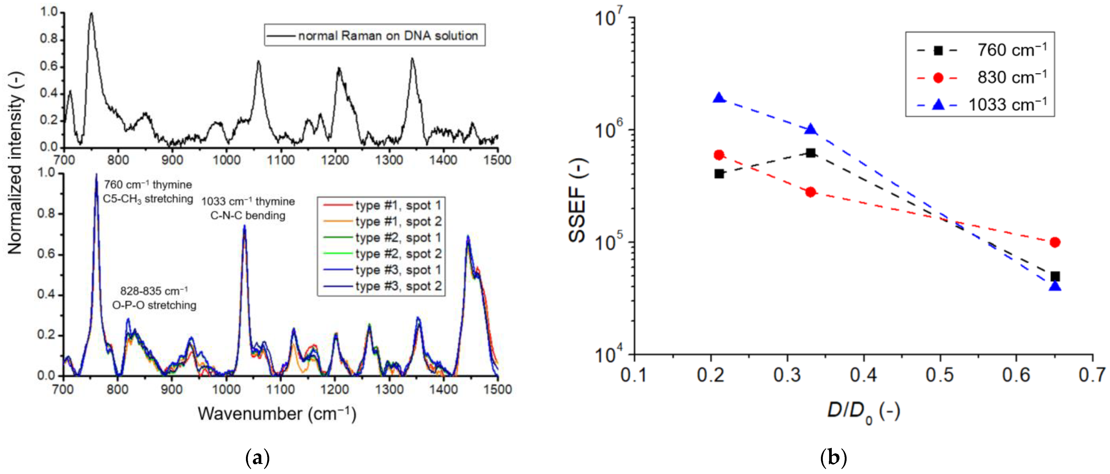
3.3. Enhancement Factor on DNA Monolayers

In order to calculate the SERS enhancement factor of the three different nanoparticle arrangements, a DNA monolayer was bound onto the surface of the gold nanoparticles, as described in Section 2.3. Here, we use the substrate-specific SERS enhancement factor (SSEF), as defined in Equation (1), which is the most convenient for surface-bound monolayers. A good comparison of the different SERS enhancement factors can be found in [24].
S S E F = I SERS I RS · N vol N surf = I SERS I RS · c sol · V ex n surf · A ex ,
Technically SSEF can be calculated from the ratio of the characteristic Raman peak intensities measured with SERS on the nanocomposite surface ( I SERS ) with normal Raman spectroscopy performed in a bulk solution of the sample ( I RS ) as a reference, taking into account the number of molecules in the two excitation volumes, N surf for SERS and N vol for normal Raman, respectively. While I SERS and I RS can be measured directly, the determination of the number of DNA molecules in the excited regions requires some elaboration. For the reference Raman measurement, the excitation volume in the solution can be estimated as a rotational ellipsoid [25], with a total volume of V ex = 34.8 μm3, calculated with the 50× objective. The DNA solution concentration ( c sol ) was controlled experimentally and was selected to be 10 mM. The focused laser beam defines the excitation area ( A ex ) for the SERS measurement. For the 100× objective used for the SERS experiments, the 0.9 μm spot diameter yielded an excitation area of 0.64 μm2. Although the surface density of DNA molecules ( n surf ) could not be determined experimentally, the resulting coverage can be estimated based on the detailed data in the literature for the same immobilization procedure [26]. Considering the ionic strength of the buffer and immobilization time, the DNA coverage was estimated to be around 3.5 × 1012 cm−2.
To prove the presence of DNA molecules on the surface of the SERS substrates, spectra were collected on the surface of the three different types in two spots each. The spectra are presented in Figure 5a, normalized to the most dominant peak at 760 cm−1. It is seen that the position of the DNA-characteristics peaks is quite well reproducible among the substrates and measurement spots. The most dominant peaks were observed for thymine at 760 cm−1 (stretching in C5-CH3), 828–835 cm−1 for phosphodiester O-P-O stretching and thymine C4-C5 stretching (combined), and 1033 cm−1 for thymine C-N-C bending [27,28]. The peaks following these can be associated with purine bases (guanine and adenine).
Although the DNA peak positions are reproducible, their intensities are subject to variation and depend strongly on how well the focal plane of the nanoparticles is matched with the focus of the laser excitation. This effect was well-characterized in our previous work. We used a z-dimensional scan mode to map the peak intensities along the normal direction (perpendicular to the substrate’s surface) with 100 nm step resolution [17]. The same z-dimensional scan was performed here to ensure that the highest possible peak intensity was used for the SSEF calculations. The resulting peak intensities of three selected characteristic vibrations (760 cm−1, 830 cm−1, and 1033 cm−1) were used to calculate the enhancement factor using Equation (1) with the experimental parameters mentioned above. The results are presented in Figure 5b in the function of the dimensionless D/D0 value.
The resulting SSEF was between 4 × 10⁴ and 2 × 10⁶ for the different particle arrangements and selected peaks. These values correspond well with the previously reported substrate-specific and analytical SERS enhancement factors [24]. By decreasing the D/D0 value from 0.65 to 0.21, both the SSEF and the Raman intensities of characteristic peaks increased by around one order of magnitude, emphasizing the importance of small interparticle gaps and hot-spot density. It should be noted that these experiments were performed on the second generation of nanocomposites with the epoxy support, and, due to the thermalization at 633 nm excitation, the measurements were performed at 785 nm laser wavelength, far from the plasmon absorption peak of the substrate. The importance of matching the excitation with the plasmon absorption is demonstrated in the next section using the third generation of nanocomposites with SiO2 support, demonstrating better thermal stability.

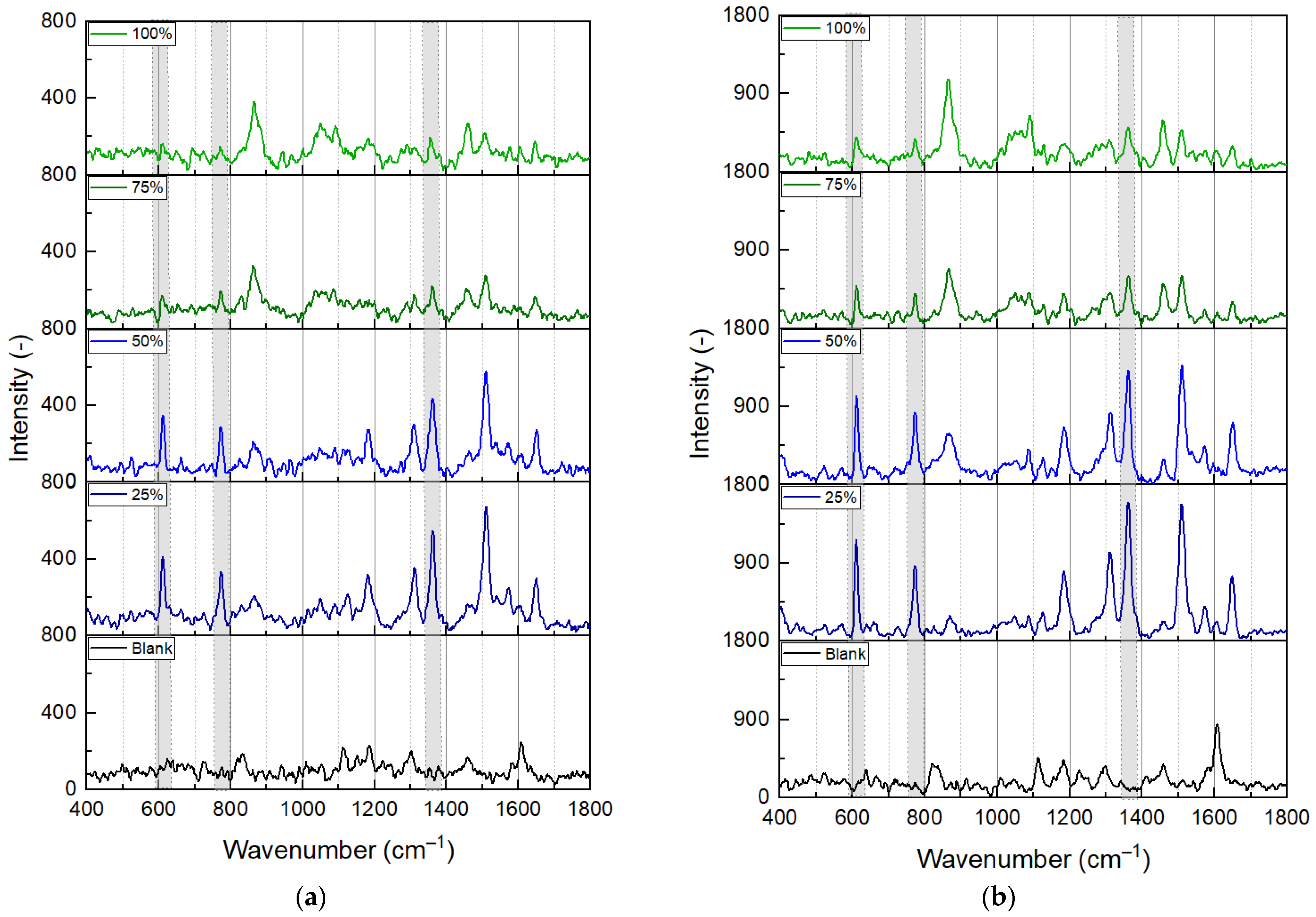
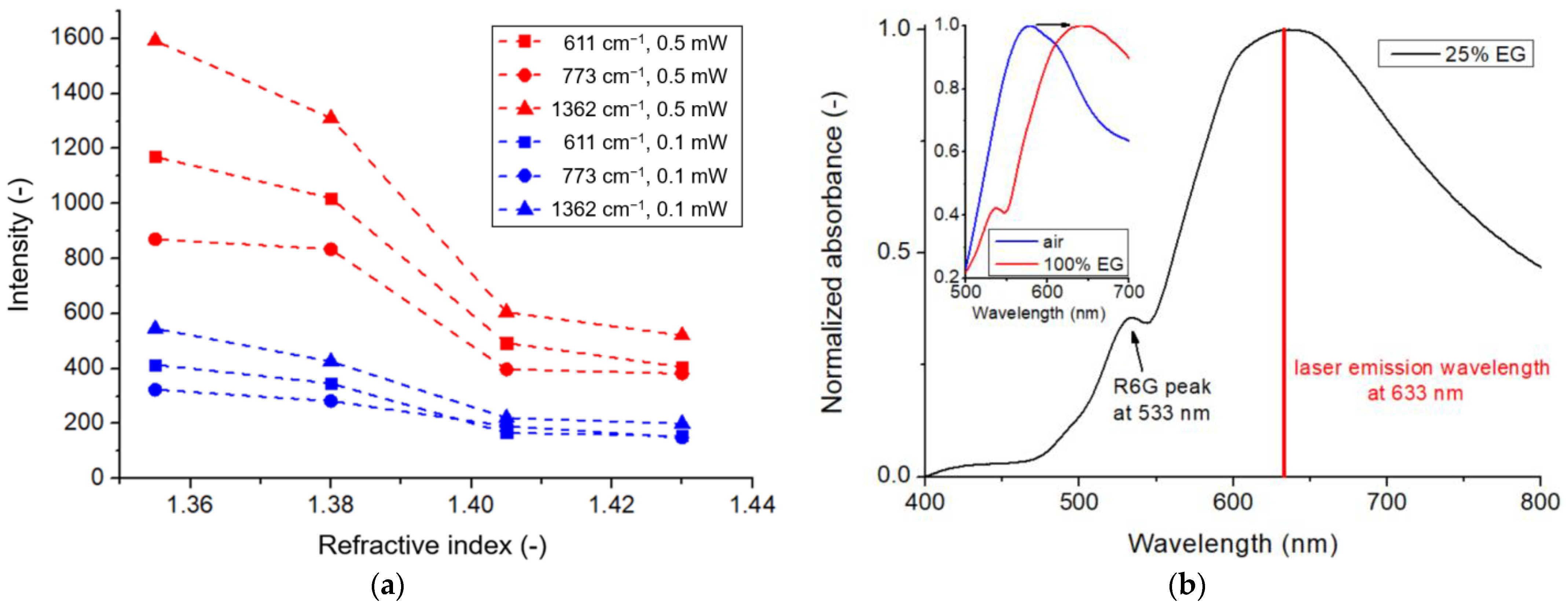
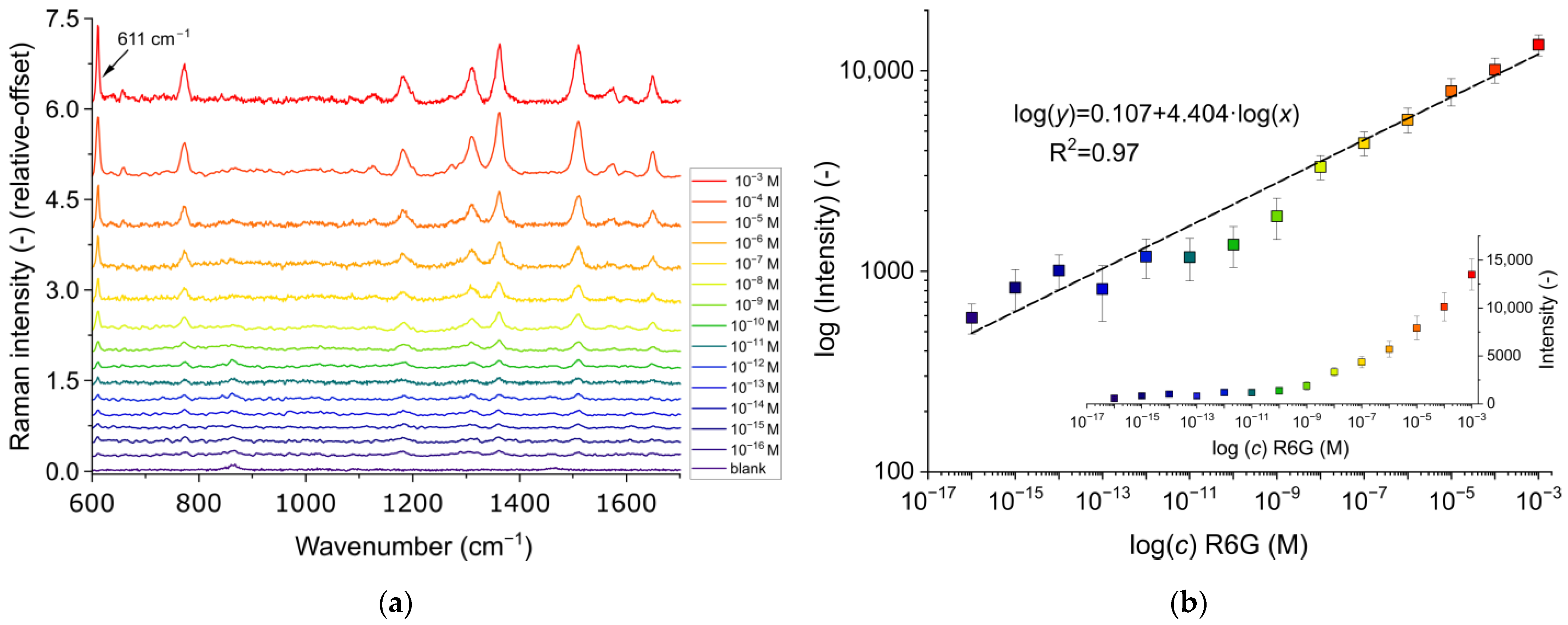
3.4. Detection of R6G in a Microfluidic Environment

In this section, the optimized detection of R6G is demonstrated with the third generation of the nanocomposite samples. For this purpose, a custom PDMS-based microfluidic cell was fabricated, as described in Section 2.4. The presented SERS experiments were performed in situ, meaning that the Raman spectra were collected while the samples were running inside the microfluidic cell.
In order to optimize the R6G detection, a set of control measurements was performed. First, we tested the effect of the laser excitation wavelength with our three available sources (532 nm, 633 nm, and 785 nm). Of the three sources, only the 633 nm excitation yielded spectra with the peaks characteristic of R6G. Considering that the relationship between the excitation wavelength and the plasmon resonance peak can play a significant role in the SERS enhancement, a measurement series was performed to fine-tune the plasmon resonance to match the 633 nm excitation by changing the refractive index of the measurement medium. This was performed by preparing different ratios of ethylene glycol (EG)/water mixtures. Measured with spectrophotometry, the plasmon absorption peak of the used type #2 nanocomposite was 579 nm in the air (directly after plasma cleaning) and 643 nm in pure EG (n = 1.4306). Based on this, the bulk refractive index sensitivity of the sample was calculated to be 154.63 nm/RIU, which can be used to estimate the plasmon peak position at different EG/water mixtures. At 25% EG content (n = 1.4306), the calculations yield ~632 nm, which would match the excitation wavelength.
To demonstrate the effect of the measurement medium’s refractive index, two experiments were performed with the 633 nm excitation at 0.1 mW and 0.5 mW laser power in different media, as illustrated in Figure 6a,b, respectively. Note that the measurements were performed in the microfluidic cell, while the laser spot was focused on the same area on the nanocomposite surface, and the solutions were pumped sequentially. The reference spectra were obtained in the air; the other four pairs were obtained in different EG/water ratios containing a fixed concentration of 1 × 10⁻⁴ M R6G. As can be seen, while the reference spectra are empty, peaks corresponding to the characteristic vibrations of R6G appear on the others, though with varying intensities. The intensities of three such peaks are plotted in Figure 7a, namely, the bending of the C-C-C ring at 611 cm−1, the out-of-plane bending of C-H at 773 cm−1, and the C-C stretching of the aromatic ring at 1362 cm−1 [29]. For both laser powers, these peaks’ intensities had a maximum of 25% EG concentration and dropped with the increasing refractive index. In Figure 6, only the peaks corresponding with EG (e.g., the C-C stretch mode at 865 cm−1 [30]) show an increasing intensity with increasing EG ratio in the mixture. The decrease in the R6G Raman peak intensities (at a fixed concentration of 1×10⁻⁴ M) is consistent with the plasmon absorbance peak’s shift away from the position of laser excitation, as illustrated in Figure 7b, with spectra measured on the same sample, in the solutions also containing the R6G molecules.
As a conclusion of these control experiments on R6G, for the determination of LOD, the 633 nm excitation was used with 0.5 mW laser power (as higher laser powers were found to damage the substrate) and in a mixture of 25% ethylene-glycol/water. In every step of the investigated concentration range, from 10−3 M to 10−16 M, spectra were gathered at five different points on the surface to test repeatability. For this reason, the sensor was removed from the microfluidic cell for this experiment, which also resulted in higher Raman intensities (owing to the absence of the calcium fluoride glass). From every concentration step, a representative spectrum is presented in Figure 8a, while the resulting characteristics are plotted in Figure 8b.
By using the characteristic R6G peak at 611 cm−1 (corresponding to the bending of the C-C-C ring), the presence of R6G was still detectable at 10−16 M concentration. It should be mentioned that, considering the mean and variation of the blank sample at this wavenumber (μblank, σblank) and the LOD = μblank + 3 × σblank rule [31], the established limit of detection can be even better, around 40 aM. This result is much better than most SERS substrates previously tested for this molecule, as summarized in Table 2. This can be attributed to two major factors: (1) In our case, the hexagonal arrangement of the particles provides high, uniform hot-spot density (nanoparticles in strong plasmonic coupling) on the surface, which is ideal for SERS; (2) matching the plasmon absorption wavelength of the substrate with the laser excitation is a critical step in the optimization of the measurement parameters, which is often neglected. As demonstrated in Figure 6 and Figure 7, increasing the gap between the laser emission and plasmon excitation wavelengths results in decreased signals and sub-optimal sensing performance.

4. Conclusions

The fabrication technology and two SERS application areas of hexagonally ordered AuNP layers on different support materials were presented. A great advantage of the proposed SERS substrate is the high hot-spot ratio on a large surface area (~ cm2 range), provided by the tightly packed nanoparticles with controlled interparticle gaps, that can also be tailored with respect to the size of the target molecules. For the three presented hexagonal NP arrangements, the interparticle gap/nanoparticle diameter ratio was controlled in the 0.21–0.65 range. Using a DNA monolayer, a substrate-specific SERS enhancement factor (SSEF) between 4 × 10⁴ and 2 × 10⁶ was demonstrated with the nanocomposites using epoxy support (second generation) and a laser excitation of 785 nm. Using SiO2 support instead of epoxy (third generation), the heat resistance of the substrates increased significantly, enabling the use of 633 nm laser excitation, directly in tune with the plasmon absorption peak of the nanocomposite. It was shown that a significant increase in the specific Raman signal could be reached by optimizing the experimental conditions by matching the plasmon absorption peak with the laser excitation. This enabled the detection of R6G molecules in a 25% ethylene-glycol/water mixture with an ultralow LOD of around 10−16 M.

Supplementary Materials

The following supporting information can be downloaded at: https://www.mdpi.com/article/10.3390/chemosensors11040235/s1, (S1) Nanoparticle Size Distribution Determination. (S2) Thermal stability of the different SERS substrates.

Author Contributions

S.Z.: investigation, visualization, writing—original draft; T.L.: investigation, methodology, writing—original draft and review; A.B. conceptualization, writing—review and editing, supervision. All authors have read and agreed to the published version of the manuscript.

Funding

This work was partially supported by the Nanoplasmonic Laser Fusion Research Laboratory project (NAPLIFE) financed by the National Research and Innovation Office (2022-2.1.1-NL-2022-00002) and by the Eötvös Lóránd Research Network (ELKH), Hungary. This research was funded by the National Research, Development, and Innovation Fund of Hungary under Grant TKP2021-EGA-02. This work was supported by the VEKOP-2.3.2-16-2016-00011 grant, which is co-financed by the European Union and European Social Fund. A. Bonyár is also grateful for the support of the Hungarian Academy of Engineering and the “MICHELBERGER MESTERDÍJ” Scholarship. Tomáš Lednický acknowledges the CzechNanoLab Research Infrastructure supported by MEYS CR (LM2018110) and support granted by the Ministry of the Interior of the Czech Republic under No. VJ01010123.

Institutional Review Board Statement

Not applicable.

Informed Consent Statement

Not applicable.

Data Availability Statement

The data presented in this study are available on request from the corresponding author.

Acknowledgments

We are grateful to Alexandra Borók, Faculty of Electrical Engineering and Informatics, Budapest University of Technology and Economics, Budapest, Hungary, for her assistance in fabricating the microfluidic cell. We also wish to express our appreciation to Miklós Veres and István Rigó, Institute for Solid State Physics and Optics, Wigner Research Centre for Physics, Budapest, Hungary, for their support and assistance during the SERS measurements.

Conflicts of Interest

The authors declare no conflict of interest.

References

  1. Azimi, S.; Docoslis, A. Recent Advances in the Use of Surface-Enhanced Raman Scattering for Illicit Drug Detection. Sensors 2022, 22, 3877. [Google Scholar] [CrossRef]
  2. Zheng, X.S.; Jahn, I.J.; Weber, K.; Cialla-May, D.; Popp, J. Label-Free SERS in Biological and Biomedical Applications: Recent Progress, Current Challenges and Opportunities. Spectrochim. Acta A Mol. Biomol. Spectrosc. 2018, 197, 56–77. [Google Scholar] [CrossRef] [PubMed]
  3. Li, X.; Blinn, K.; Chen, D.; Liu, M. In Situ and Surface-Enhanced Raman Spectroscopy Study of Electrode Materials in Solid Oxide Fuel Cells. Electrochem. Energy Rev. 2018, 1, 433–459. [Google Scholar] [CrossRef]
  4. Moisoiu, V.; Iancu, S.D.; Stefancu, A.; Moisoiu, T.; Pardini, B.; Dragomir, M.P.; Crisan, N.; Avram, L.; Crisan, D.; Andras, I.; et al. SERS Liquid Biopsy: An Emerging Tool for Medical Diagnosis. Colloids Surf. B Biointerfaces 2021, 208, 112064. [Google Scholar] [CrossRef]
  5. Fales, A. SERS for Point-of-Care and Clinical Applications; Elsevier: Amsterdam, The Netherlands, 2022; pp. 1–243. [Google Scholar] [CrossRef]
  6. Chakraborty, I.; Banik, S.; Biswas, R.; Yamamoto, T.; Noothalapati, H.; Mazumder, N. Raman Spectroscopy for Microplastic Detection in Water Sources: A Systematic Review. Int. J. Environ. Sci. Technol. 2022, 1–14. [Google Scholar] [CrossRef]
  7. Terry, L.R.; Sanders, S.; Potoff, R.H.; Kruel, J.W.; Jain, M.; Guo, H. Applications of Surface-Enhanced Raman Spectroscopy in Environmental Detection. Anal. Sci. Adv. 2022, 3, 113–145. [Google Scholar] [CrossRef]
  8. Xu, M.L.; Gao, Y.; Han, X.X.; Zhao, B. Innovative Application of SERS in Food Quality and Safety: A Brief Review of Recent Trends. Foods 2022, 11, 2097. [Google Scholar] [CrossRef]
  9. Fleischmann, M.; Hendra, P.J.; McQuillan, A.J. Raman Spectra of Pyridine Adsorbed at a Silver Electrode. Chem. Phys. Lett. 1974, 26, 163–166. [Google Scholar] [CrossRef]
  10. Mosier-Boss, P.A. Review of SERS Substrates for Chemical Sensing. Nanomaterials 2017, 7, 142. [Google Scholar] [CrossRef] [Green Version]
  11. Lin, C.; Liang, S.; Peng, Y.; Long, L.; Li, Y.; Huang, Z.; Long, N.V.; Luo, X.; Liu, J.; Li, Z.; et al. Visualized SERS Imaging of Single Molecule by Ag/Black Phosphorus Nanosheets. Nano-Micro Lett. 2022, 14, 1–15. [Google Scholar] [CrossRef]
  12. Qiu, Y.; Kuang, C.; Liu, X.; Tang, L. Single-Molecule Surface-Enhanced Raman Spectroscopy. Sensors 2022, 22, 4889. [Google Scholar] [CrossRef] [PubMed]
  13. Pilot, R.; Signorini, R.; Durante, C.; Orian, L.; Bhamidipati, M.; Fabris, L. A Review on Surface-Enhanced Raman Scattering. Biosensors 2019, 9, 57. [Google Scholar] [CrossRef] [Green Version]
  14. Jeanmaire, D.L.; van Duyne, R.P. Surface Raman Spectroelectrochemistry. J. Electroanal. Chem. Interfacial Electrochem. 1977, 84, 1–20. [Google Scholar] [CrossRef]
  15. Šubr, M.; Procházka, M. Polarization- and Angular-Resolved Optical Response of Molecules on Anisotropic Plasmonic Nanostructures. Nanomaterials 2018, 8, 418. [Google Scholar] [CrossRef] [PubMed] [Green Version]
  16. Lednický, T.; Bonyár, A. Large Scale Fabrication of Ordered Gold Nanoparticle-Epoxy Surface Nanocomposites and Their Application as Label-Free Plasmonic DNA Biosensors. ACS Appl. Mater. Interfaces 2020, 12, 4804–4814. [Google Scholar] [CrossRef] [Green Version]
  17. Bonyár, A.; Zangana, S.; Lednický, T.; Rigó, I.; Csarnovics, I.; Veres, M. Application of Gold Nanoparticles–Epoxy Surface Nanocomposites for Controlling Hotspot Density on a Large Surface Area for SERS Applications. Nano-Struct. Nano-Objects 2021, 28, 100787. [Google Scholar] [CrossRef]
  18. Borók, A.; Laboda, K.; Bonyár, A. PDMS Bonding Technologies for Microfluidic Applications: A Review. Biosensors 2021, 11, 292. [Google Scholar] [CrossRef]
  19. Bonyár, A. Maximizing the Surface Sensitivity of LSPR Biosensors through Plasmon Coupling—Interparticle Gap Optimization for Dimers Using Computational Simulations. Biosensors 2021, 11, 527. [Google Scholar] [CrossRef]
  20. Li, J.; Ye, J.; Chen, C.; Li, Y.; Verellen, N.; Moshchalkov, V.V.; Lagae, L.; Van Dorpe, P. Revisiting the Surface Sensitivity of Nanoplasmonic Biosensors. ACS Photonics 2015, 2, 425–431. [Google Scholar] [CrossRef] [Green Version]
  21. Bonyár, A.; Lednický, T.; Hubálek, J. LSPR Nanosensors with Highly Ordered Gold Nanoparticles Fabricated on Nanodimpled Aluminium Templates. Procedia Eng. 2016, 168, 1160–1163. [Google Scholar] [CrossRef]
  22. Millet, L.J.; Jain, A.; Gillette, M.U. Less Is More: Oligomer Extraction and Hydrothermal Annealing Increase PDMS Bonding Forces for New Microfluidics Assembly and for Biological Studies. bioRxiv 2017, 150953. [Google Scholar] [CrossRef]
  23. Yunus, S.; de Crombrugghe De Looringhe, C.; Poleunis, C.; Delcorte, A. Diffusion of Oligomers from Polydimethylsiloxane Stamps in Microcontact Printing: Surface Analysis and Possible Application. Surf. Interface Anal. 2007, 39, 922–925. [Google Scholar] [CrossRef]
  24. le Ru, E.C.; Blackie, E.; Meyer, M.; Etchegoint, P.G. Surface Enhanced Raman Scattering Enhancement Factors: A Comprehensive Study. J. Phys. Chem. C 2007, 111, 13794–13803. [Google Scholar] [CrossRef]
  25. Rzhevskii, A. Basic Aspects of Experimental Design in Raman Microscopy. Spectroscopy 2016, 31, 40–45. [Google Scholar]
  26. Gong, P.; Levicky, R. DNA Surface Hybridization Regimes. Proc. Natl. Acad. Sci. USA 2008, 105, 5301–5306. [Google Scholar] [CrossRef] [Green Version]
  27. Sagar, D.M.; Korshoj, L.E.; Hanson, K.B.; Chowdhury, P.P.; Otoupal, P.B.; Chatterjee, A.; Nagpal, P. High-Throughput Block Optical DNA Sequence Identification. Small 2018, 14, 1703165. [Google Scholar] [CrossRef]
  28. Kim, J.; Park, H.J.; Kim, J.H.; Chang, B.; Park, H.K. Label-free Detection for a DNA Methylation Assay Using Raman Spectroscopy. Chin. Med. J. 2017, 130, 1961–1967. [Google Scholar] [CrossRef]
  29. Huang, D.; Cui, J.; Chen, X. A Morpholinium Surfactant Crystallization Induced Formation of Au Nanoparticle Sheet-like Assemblies with Uniform SERS Activity. Colloids Surf. A Phys. Eng. Asp. 2014, 456, 100–107. [Google Scholar] [CrossRef]
  30. Gontrani, L.; Tagliatesta, P.; Agresti, A.; Pescetelli, S.; Carbone, M. New Insights into the Structure of Glycols and Derivatives: A Comparative X-Ray Diffraction, Raman and Molecular Dynamics Study of Ethane-1,2-Diol, 2-Methoxyethan-1-Ol and 1,2-Dimethoxy Ethane. Crystals 2020, 10, 1011. [Google Scholar] [CrossRef]
  31. McNaught, A.D.; Wilkinson, A. Compendium of Chemical Terminology-Gold Book; IUPAC: Research Triangle Park, NC, USA, 2012; p. 1670. [Google Scholar] [CrossRef]
  32. Zhao, N.; Li, H.; Tian, C.; Xie, Y.; Feng, Z.; Wang, Z.; Yan, X.; Wang, W.; Yu, H. Bioscaffold Arrays Decorated with Ag Nanoparticles as a SERS Substrate for Direct Detection of Melamine in Infant Formula. RSC Adv. 2019, 9, 21771–21776. [Google Scholar] [CrossRef] [Green Version]
  33. Wu, H.Y.; Lin, H.C.; Hung, G.Y.; Tu, C.S.; Liu, T.Y.; Hong, C.H.; Yu, G.; Hsu, J.C. High Sensitivity SERS Substrate of a Few Nanometers Single-Layer Silver Thickness Fabricated by DC Magnetron Sputtering Technology. Nanomaterials 2022, 12, 2742. [Google Scholar] [CrossRef] [PubMed]
  34. Wu, H.Y.; Lin, H.C.; Liu, Y.H.; Chen, K.L.; Wang, Y.H.; Sun, Y.S.; Hsu, J.C. Highly Sensitive, Robust, and Recyclable TiO2/AgNP Substrate for SERS Detection. Molecules 2022, 27, 6755. [Google Scholar] [CrossRef] [PubMed]
  35. Chiang, C.Y.; Liu, T.Y.; Su, Y.A.; Wu, C.H.; Cheng, Y.W.; Cheng, H.W.; Jeng, R.J. Au Nanoparticles Immobilized on Honeycomb-Like Polymeric Films for Surface-Enhanced Raman Scattering (SERS) Detection. Polymers 2017, 9, 93. [Google Scholar] [CrossRef] [Green Version]
  36. Choi, C.J.; Xu, Z.; Wu, H.Y.; Liu, G.L.; Cunningham, B.T. Surface-Enhanced Raman Nanodomes. Nanotechnology 2010, 21, 415301. [Google Scholar] [CrossRef] [PubMed]
  37. Fu, H.; Chen, J.; Chen, L.; Zhu, X.; Chen, Z.; Qiu, B.; Lin, Z.; Guo, L.; Chen, G. A Calcium Alginate Sponge with Embedded Gold Nanoparticles as a Flexible SERS Substrate for Direct Analysis of Pollutant Dyes. Microchim. Acta 2019, 186, 1–7. [Google Scholar] [CrossRef]
  38. Liu, R.; Zha, Z.; Li, C.; Shafi, M.; Peng, Q.; Liu, M.; Zhang, C.; Du, X.; Jiang, S. Coupling of Multiple Plasma Polarization Modes in Particles–Multilayer Film System for Surface-Enhanced Raman Scattering. APL Photonics 2021, 6, 036104. [Google Scholar] [CrossRef]
  39. Zhang, W.; Zhu, X.; Chen, Z.; Belotelov, V.I.; Song, Y. Silver Nanopillar Arrayed Thin Films with Highly Surface-Enhanced Raman Scattering for Ultrasensitive Detection. ACS Omega 2022, 7, 25726–25731. [Google Scholar] [CrossRef]
  40. Wang, J.; Qiu, C.; Mu, X.; Pang, H.; Chen, X.; Liu, D. Ultrasensitive SERS Detection of Rhodamine 6G and P-Nitrophenol Based on Electrochemically Roughened Nano-Au Film. Talanta 2020, 210, 120631. [Google Scholar] [CrossRef]
  41. Hamzah, F.G.; Humud, H.R. The Raspberry-like Nanostructures (SiO2@AgNPs) Fabricated by Electrical Exploding Wire (EEW) Technique for Raman Scattering Enhancement. AIP Conf. Proc. 2020, 2290, 050033. [Google Scholar] [CrossRef]
  42. Xu, D.; Zhang, Y.; Zhang, S.; Yang, W.; Wang, Z.; Li, J. Copper Nanoleaves SERS Substrates with High Surface Roughness for Sensitive Detection Crystal Violet and Rhodamine 6G. Opt. Laser Technol. 2022, 145, 107502. [Google Scholar] [CrossRef]
  43. Zhu, J.; Lin, G.; Wu, M.; Chen, Z.; Lu, P.; Wu, W. Large-Scale Fabrication of Ultrasensitive and Uniform Surface-Enhanced Raman Scattering Substrates for the Trace Detection of Pesticides. Nanomaterials 2018, 8, 520. [Google Scholar] [CrossRef] [PubMed] [Green Version]
  44. He, L.; Huang, J.; Xu, T.; Chen, L.; Zhang, K.; Han, S.; He, Y.; Lee, S.T. Silver Nanosheet-Coated Inverse Opal Film as a Highly Active and Uniform SERS Substrate. J. Mater. Chem. 2011, 22, 1370–1374. [Google Scholar] [CrossRef]
  45. Yang, W.; Ou, Q.; Li, C.; Cheng, M.; Li, W.; Liu, Y. Ultrasensitive Flower-like TiO2/Ag Substrate for SERS Detection of Pigments and Melamine. RSC Adv. 2022, 12, 6958–6965. [Google Scholar] [CrossRef] [PubMed]
Figure 1. A comprehensive illustration of fabrication technologies towards gold nanoparticle nanocomposites. (1–4) Fabrication of nanobowled aluminum templated for controlled synthesis of gold nanoparticles (AuNPs) by (4–6) a solid-state dewetting (SSD) of the thin gold film. (6–8) Transfer of AuNPs on various substrates and (8–9) their exposure by reactive ion etching (RIE) of substrates. Three generations of nanocomposites are compared in this work using (7a–9a) PDMS, epoxy, and (7b–9b) SiO2 as a substrate.
Chemosensors 11 00235 g001
Figure 2. Photographs of three generations of AuNP nanocomposites.
Chemosensors 11 00235 g002
Figure 3. Photograph of the assembled microfluidic chip with the SERS substrate in the middle with a schematic cross-sectional illustration of the microfluidic cell in the bottom.
Chemosensors 11 00235 g003
Figure 4. Top: SEM images of three different AuNP arrangements (type #1, #2, and #3) over the aluminum template (Figure 1: 6). Bottom: STEM (BF) images of the same AuNP arrangements as a final sensor element on SiO2 nanopillars/substrate (Figure 1: 9b). In STEM images the aluminum layer (~300 nm) can be seen covering AuNPs and partly filling gaps between SiO2 pillars. The Al layer was used to prepare lamellae of ~100 nm thickness.
Chemosensors 11 00235 g004
Figure 5. (a) Top: Raman spectrum measured on a 10 mM DNA sample in solution. Bottom: SERS spectra were obtained on three different substrates containing three different nanoparticle arrangements (type #1, #2, and #3, respectively). The spectra are baseline corrected and normalized to the peak intensity at 760 cm−1. On every substrate, two spectra obtained in different spots are presented. (b) The substrate-specific SERS enhancement factor (SSEF) values, calculated for the three different nanoparticle arrangements, in the function of the dimensionless D/D0 value, for three characteristic DNA-related peaks.
Chemosensors 11 00235 g005
Figure 6. SERS spectra were obtained on a type #2 substrate with 633 nm excitation at different conditions. (a) 0.1 mW laser power, (b) 0.5 mW laser power. The reference was measured in air, without any sample in the microfluidic cell. The other spectra were obtained in ethylene-glycol/water mixtures in different ratios (25%, 50%, 75%, and 100%) containing 1 × 10⁻⁴ M R6G. The presented spectra are baseline corrected. The vertical dashed lines and shadowed areas mark the three peaks characteristic of R6G that were used for further evaluation.
Chemosensors 11 00235 g006
Figure 7. (a) Relative SERS intensities corresponding to characteristic peaks of the R6G molecules, measured at 633 nm excitation with 0.1 mW and 0.5 mW laser power, respectively. The data correspond with the spectra presented in Figure 5. (b) Normalized absorption spectrum of the type #2 substrate in 25% ethylene-glycol/water mixture, containing 1 × 10⁻⁴ M R6G. The insert shows the shift between air (n = 1) and 100% EG (n = 1.4306).
Chemosensors 11 00235 g007
Figure 8. (a) Raman spectra measured on a type #2 substrate in a 25% ethylene-glycol/water mixture with different R6G concentrations, from 10−3 M to 10−16 M. The spectra are all baseline corrected and stacked on top of each other for the sake of presentation only. (b) The static characteristic of R6G determination calculated from the Raman intensity of the peak at 611 cm−1. Every measurement point is an average of data obtained in five different points on the surface with standard deviation. The color scheme of different concentrations corresponds to the right figure (a). The top plot is in log-log scale with linear fitting; the insert in the bottom is in linear-log scale.
Chemosensors 11 00235 g008
Table 1. Distribution parameters of AuNP arrangements.
TypeSize of AuNPsThicknessD/D0Defects per Particle
#1(67.4 ± 2.9) nm ~25 nm0.65 ± 0.120.9 %
#2(83.2 ± 3.4) nm~35 nm0.33 ± 0.103.2 %
#3(91.5 ± 4.2) nm~45 nm0.21 ± 0.097.0 %
Table 2. Comparison of LOD of R6G detection for different SERS substrates.
SERS Substrate TypeLODReference
Bioscaffold arrays decorated with silver nanoparticles (AgNPs)10−7[32]
Few nm thick silver layer, deposited with sputtering 10−8[33]
TiO2/Ag NP composite substrate10−8[34]
Honeycomb-like polymeric films filled with AuNPs10−8[35]
Silver coated nanodomes10−9[36]
AuNPs embedded in a calcium alginate sponge10−10[37]
A hybrid AgNP/ AuNP /Al2O3 multilayer film10−10[38]
Silver nanopillar arrayed thin films10−10[39]
Electrochemically roughened Au film10−11[40]
Raspberry-like SiO2@AgNPs nanostructures10−12[41]
Dendritic copper nanoleaves10−13[42]
Uniform AgNP array on a glass/PDMS substrate10−14[43]
Silver nanosheet-coated inverse opal film10−14[44]
Flower-like TiO2/Ag nanostructure5 × 10−16[45]
Hexagonally ordered AuNP layers on SiO210−16this work
Ag nanoparticles embedded in multi-layer black phosphorus nanosheets10−20
(single molecule)
[11]
Disclaimer/Publisher’s Note: The statements, opinions and data contained in all publications are solely those of the individual author(s) and contributor(s) and not of MDPI and/or the editor(s). MDPI and/or the editor(s) disclaim responsibility for any injury to people or property resulting from any ideas, methods, instructions or products referred to in the content.

