Abstract
Orthogonal reheating double-pulse laser-induced breakdown spectroscopy (LIBS) was applied to the elemental analysis of CdTe thin film samples. Films were grown through nanosecond pulsed laser ablation over silicon and glass substrates. The analysis was performed by applying a 266 nm pulsed laser devised to minimize sample damage. Re-excitation was conducted using a nanosecond laser emitting at 1064 nm that induced air breakdown 1 mm above the target. Emission enhancement was investigated as a function of both time acquisition delay and inter-pulse delay. The plasma temperature and electron density calculations made showed that the double-pulse scheme produced higher temperature values and a longer plasma duration than single-pulse LIBS. The self-absorption coefficient of the lines was determined from the measured ablated matter, plasma volume and collected spectra. The results of the double-pulse LIBS configuration showed a significant increase in emission intensity, reducing the self-absorption effect. In addition, the relative concentration of the thin films was determined for both experimental schemes. The calculated elemental values for the double-pulse configuration coincide with those expected and are more accurate than those obtained using a single laser.
1. Introduction
Cadmium telluride thin films are being investigated for applications including optoelectronic devices and photovoltaic cell fabrication [1,2]. In particular, its direct band gap close to ~1.5 is suitable for efficient solar energy conversion [3]. Moreover, conversion efficiencies in excess of 21% and solar irradiation absorption up to 90% have been achieved using films with a thickness of 1 µm [1,4]. CdTe films have been grown using several techniques, such as electrodeposition, spray pyrolysis, sputtering and pulsed laser deposition [4,5,6]. The chemical characterization of thin films is of great importance because their growth is not always stoichiometric [7]. Therefore, several techniques have been applied to investigate their composition, including secondary ion mass spectrometry, X-ray photoelectron spectroscopy, energy dispersive X-ray spectroscopy, Rutherford backscattering, etc. [8]. However, these techniques require that samples be placed in a vacuum and have specific dimensions and geometries.
On the other hand, laser-produced plasmas have been used for different applications, from elemental characterization to nanoparticle production and thin films [9,10,11,12]. In particular, laser-induced breakdown spectroscopy (LIBS) is an analytical technique that allows the elemental analysis of a large variety of samples requiring little or no sample preparation at a relatively low cost. Moreover, this technique is also portable, allowing fast sample characterization with high spatial resolution [13,14,15]. LIBS has a very wide range of applications and can be applied in harsh environments for the remote analysis of samples [13,15,16,17,18,19,20,21]. LIBS has also been applied to surface analysis, to investigate different types of coatings using depth profiling [22,23,24,25,26,27]. However, its main limitation is the low pulse-to-pulse signal reproducibility and limited sensibility compared to other established techniques [28]. Thus, to avoid spectral fluctuations and to increase the signal-to-noise ratio, the averaging of several spectra is usually employed [29]. In addition, to reduce the limit of detection of traces, several alternatives have been implemented to enhance the LIBS signal. These include the use of microwaves to re-excite the ablation plasma, high voltage discharges, magnetic confinement and double pulse re-excitation, among others [30].
In double pulse configuration (DP-LIBS) there are two basic experimental arrangements: in one of them, both pulses ablate the sample; in the other, one of the pulses produces the breakdown of air close to the ablation point. The latter configuration has the advantage that the air-produced plasma does not remove additional material from the sample. In particular, when re-excitation is applied after a low-irradiance ablation plasma, intensifications of two orders of magnitude can be achieved [31]; but this scheme is not commonly employed.
LIBS can be a feasible alternative for the analysis of the composition and morphology of thin films. In addition, when films are grown using the pulsed laser deposition (PLD) technique, analysis can be quickly performed within the laboratory and using the same pulsed laser. There have been some studies in which this issue has been addressed with results that are in agreement with those obtained using other analysis techniques [32,33,34,35,36,37]. However, the ablation energies used were relatively large (10–200 mJ), producing craters from hundreds of micrometers up to 1 mm in diameter. On the other hand, low-energy femtosecond pulse lasers have been used to reduce sample damage; but these lasers are significantly more expensive [38,39]. In the work of Nishijima et al. [40], a modification of the collinear DP-LIBS was employed for thin film analysis. In this paper, the emission from two 115 mJ lasers was concentrated at spots spaced about 1 mm apart. Line intensities increased significantly compared to those obtained using DP-LIBS or single pulse configurations; however, in this proposed setup, the damage to the sample was increased. This is due to the fact that the ablation was performed at two separate points, removing a relatively large area of the film.
In the present work, the use of two nanosecond-delayed laser pulses in an orthogonal reheating configuration was proposed to investigate the relative composition of CdTe thin films. In this scheme, the first pulse was focused on the thin film, while the second laser pulse produced a plasma that re-excited the ablated matter. This configuration allowed the use of low energy for sample ablation and high energy for re-excitation, thus minimizing damage to the target.
2. Materials and Methods
2.1. Experimental Procedure
Figure 1 shows the orthogonal double-pulse LIBS experimental setup in the reheating configuration (DP-LIBS) used in this work. Ablation of the samples was performed using a high-power pulsed Nd: YAG laser (Q-Smart 100, from Quantel) emitting 5 ns pulses at 266 nm (fourth harmonic). The laser frequency was kept fixed at 1 Hz, while the energy was varied within the range of 0.5–9 mJ. The beam of the UV pulse was focused with a plano-convex quartz lens having a nominal focal length of 50.2 mm. This corresponds to 42 mm measured from the back focal length for the 266 nm wavelength, thus generating a spot of about 20 μm in diameter at the lens focal distance. The initial plasma was reheated using a second Nd:YAG laser (Brilliant Eazy, from Quantel) emitting 5 ns pulses at a wavelength of 1064 nm, and the energy was kept fixed at 30 mJ. The delay time between the formation of both plasmas varied between 100 ns and 500 μs. The beam of the reheating laser was focused parallel to the sample’s surface using a 100 mm focal length plano-convex lens, forming plasma in the air at a variable height from the sample surface. After an optimization process, the distance perpendicular to the surface was set to 1 mm, which maximized the emission intensification without increasing the removed mass.
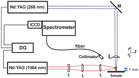
Figure 1.
Experimental arrangement employed for orthogonal DP-LIBS in reheating configuration. Key: L: lens; M: mirror; PD: photodiode; DG: pulse/delay generator; Scope: oscilloscope.
Spatially integrated light was collected through a quartz collimator with a focal length of 10 mm, placed at approximately 45° with respect to the sample. Then, light was sent through a 200 μm optical fiber bundle to a 50 cm Czerny–Turner spectrograph (Spectra Pro 2500i, from Acton Research) equipped with 600 and 1800 line/mm gratings. Spectra were finally detected with an ICCD camera (PiMAX 1024 × 1024, from Princeton Instruments). The calculated instrumental broadening using the 1800 l/mm grating was 0.05 nm.
Both lasers and the ICCD camera were externally triggered using an 8-channel delay generator (575-8C, from Berkeley Nucleonics). For time-integrated experiments, the ICCD exposure time was set to 30 μs, while the time delay was varied from 20 ns to 1000 ns for the single-pulse ablation experiment (SP-LIBS), and from 100 ns to 60 µs for the double-pulse case (DP-LIBS). For time-resolved analysis, the acquisition time was 100 ns.
Plasma dimensions were obtained via shadowgraphy [41,42]. For this purpose, the beam of a continuous diode laser emitting at 405 nm was expanded and collimated. Then, the beam was steered along the z-direction, perpendicular to the direction of both pulsed lasers, and the light was projected onto a screen. Images of the shadow produced by the plasma were then captured using the ICCD camera through a Nikon lens. In these experiments, the camera shutter time was 100 ns, and images were acquired with delays from the plasma onset up to 15 µs. Finally, the dimensions and the plasma volumes were obtained assuming cylindrical symmetry.
2.2. Samples
The investigated samples were six CdTe thin films grown either on glass (four samples) or on crystalline silicon substrate (two samples). The growth was carried out via pulsed laser deposition (PLD) in vacuum, using a 99.999% CdTe sputtering target from Lesker. Briefly, films were grown by irradiating with 1064 nm pulses a CdTe target with a laser fluence of 10 J/cm2 for 20–40 min. The distance from the target to the substrate was 10 cm, and the substrate temperature was maintained at 200 °C; further details can be found in our previous work [43]. X-Ray diffraction analysis showed that CdTe coating is polycrystalline with a Zinc-Blende-type crystalline structure, and preferential orientation in the (111) plane. Film thicknesses were obtained through profilometry analysis, with values ranging from 150 to 260 nm.
2.3. Methodology
For a plasma under local thermodynamic equilibrium, the emissivity of a transition belonging to a chemical element i with ionic state z (z = 0 and z = 1 correspond to neutral and singly ionized atoms) can be written as:
where the subscripts k and j indicate the upper and lower energy levels, h is the Planck constant, c is the speed of light, is the probability of transition from state k to state j, is the wavelength, is the density number of emitting species, is the partition function at the temperature T, is the level degeneracy and is the Boltzmann constant.
To determine the relative composition of an unknown sample α, we proceeded by dividing the intensity of a line of this sample with respect to the value obtained for a reference sample r [33]; this ratio is written in terms of Equation (1). For stoichiometric ablation, the composition of the plasma represents the target composition. Further, assuming that the experiments performed on both targets have the same plasma temperature, as previously reported [27], it follows that: Iα/Ir = Nα/Nr, where I is the line intensity.
In our case, the CdTe sputtering target is used as the reference, and the thin film is the unknown sample. Finally, the quotient of the concentrations of two chemical elements i (1,2) in a sample r can be written in terms of the values obtained for the unknown sample α [33]:
Here, the emission intensities and species density values correspond to cadmium and tellurium. From Equation (2), note that the relative concentration of Cd and Te in thin films can be obtained by measuring the emission intensities (area under the line) of two transitions belonging to the investigated elements.
For a correct determination of this ratio, the possible self-absorption of emission lines must be taken into account. The self-absorption coefficient (SA) is given by [44,45]:
where l is the plasma length. The absorption coefficient k can be written as:
where is the central wavelength of the transition and Δλ is the full width at half maximum (FWHM) of the line. Here, it is assumed that the line has a Lorentzian profile, which is true when the line broadening is dominated by the Stark effect. Thus, when self-absorption is negligible, kl ≪ 1 and SA ≈ 1.
The plasma temperature and electron density are needed to estimate SA values. The electron density can be obtained by measuring the FWHM of an optically thin line after subtracting the instrumental broadening contribution through [15]:
where the is the measured value and is the Stark broadening parameter obtained at FWHM at a reference electron density .
The plasma temperature was obtained from the multi-element Saha–Boltzmann plots proposed by Aguilera and Aragón [46]. This is a modification of the usual Boltzmann plot used in LIBS. In this formulation, the graphs are modified considering the relations between the populations for neutral and ionic species, considering the concentration of the different elements present in the sample. In this variation of the Boltzmann method, the temperature was determined from the following equation:
where the subindex i indicates the element used (in this work, Cd and Te), m is the electron mass, is the elemental concentration, is the ionization energy and N is the total number density. In this expression, only neutral and ionic species were taken into account. Finally, the ratio of the ionic to neutral atom number densities is written as follows:
where is the correction to the ionization energy due to interactions within the plasma.
Using a guess value for the temperature on the left-hand side of Equation (6), it was possible to construct a graph similar to the usual Boltzmann plot. In this way, it was possible to perform an iterative method in which the plasma temperature was obtained using spectral lines corresponding to different chemical elements.
3. Results and Discussion
3.1. Optimization of the Experimental Parameters
Preliminary experiments using the single-pulse configuration have shown that the area of film removed increases with laser energy when keeping the distance from the lens to the target constant. The diameter of the removed film can reach several hundred micrometers, at laser energies of 9 mJ. In addition, since the depth produced by a single shot is about 1 µm, the entire film was always removed. Finally, it was decided to use ablation energy of 0.5 mJ to minimize the damage to the film. Figure 2 shows a profilometer scan of craters produced by the single-shot impact on two thin films: one, 260 nm thick, grown on silicon, and the other, 184 nm thick, grown on glass.
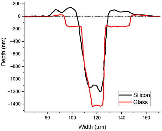
Figure 2.
Profilometer scan corresponding to a crater produced by a 0.5 mJ single shot on CdTe thin films grown on silicon substrate and glass.
As can be observed in Figure 2, the removed diameter measured at the surface level for films grown on silicon is about 25 µm, which is near the calculated value of 20 µm for the employed experimental conditions. On the other hand, films grown over glass showed an increased film area removal. This may be related to the lower adhesion of the films on this substrate compared to silicon.
The next step was to find the best experimental conditions to maximize the LIBS signal. The spectral region spanning 212–255 nm was selected, which allowed simultaneous observation of several cadmium and tellurium transitions. Next, we proceeded to perform the LIBS signal optimization process for the single pulse experiment to maximize the signal-to-noise ratio (SNR) using 0.5 mJ to ablate the target. To minimize damage to the films, this procedure was performed on the CdTe sputtering target by acquiring 20 single-shot spectra for each condition. Each emission line was fitted with a Lorentzian profile, and the SNR was obtained from the ratio between the height of the line and the noise adjacent to it. The emission was both spatially and temporally integrated, and the acquisition delay was varied in the range of 20 to 1000 ns, yielding the maximum SNR value with a delay of 70 ns. This is a relatively short delay for LIBS with nanosecond pulse, but note that the deposited energy was relatively low.
The signal optimization process was also performed for the DP-LIBS experiment in the orthogonal reheating configuration. In these experiments, the SNR was investigated as a function of the ICCD acquisition delay after the second pulse (12 different delays from 100 ns to 5 µs) and for various delays among the pulses (10 delays from 0 to 60 µs). It was found that the optimum delay after the second pulse is about 700 ns. Subsequently, the emission intensification was obtained as the ratio between the SNR for DP-LIBS and the best SNR value obtained for the SP-LIBS arrangement. Thus, using the optimized delays for both conditions, the improvement in the SNR was studied by varying the delay between pulses (see Figure 3). As can be seen, for a large range of inter-pulse delays, an increase in SNR is observed for all cadmium lines. This is an indication that the employed re-excitation configuration works according to the desired objectives, increasing the observed signal significantly. However, the neutral Te transitions show that the intensity does not improve. This was previously reported by Gautier et al. [47,48], where it was observed that the emission lines that are most favored in the re-excitation process are those with higher excitation levels [49]. Similarly, a possible increase in the temperature of the ablation plasma can lead to the population of ionic species being favored, causing the neutral lines to show a decrease in the detected signal.
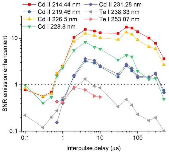
Figure 3.
Signal-to-noise emission intensification for the orthogonal reheating double-pulse experiment as a function of the interpulse delay. The ICCD acquisition delay is 700 ns after the second pulse and the gate width is 30 µs.
From the above, it was decided for subsequent experiments to use a delay between pulses of 4 µs, since it obtained the maximum intensity value for neutral transitions as well as for ionic species. Under these conditions, the spectra shown in Figure 4 were acquired, where a comparison of the intensities obtained for SP-LIBS and DP-LIBS is made. This figure was obtained from a single shot on a thin film grown on silicon with a thickness of 245 nm. As can be seen in the SP-LIBS configuration, some transitions have very low-intensity values, while others could only be observed when DP-LIBS was used, for instance, the 219.46 nm line belonging to Cd II.
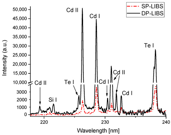
Figure 4.
Comparison of time-integrated spectra obtained for SP-LIBS and DP-LIBS obtained from a single shot over a thin film target.
3.2. Plasma Characterization
To select optically thin transitions for the calculation of thin film composition through LIBS, it was first necessary to determine the plasma temperature and electron density. Spectra were obtained using the 1800 l/mm diffraction grating, allowing us to observe the spectral region 225–239 nm. Since this investigation was conducted as a function of time, this analysis was also performed using the certified CdTe target to avoid damaging the thin films.
The electron density was calculated using the broadening of spectral lines, dominated by the Stark effect. Lines were fitted with a Lorentzian distribution to obtain the FWHM. Afterward, the contribution due to instrumental broadening was subtracted from the line broadening. The electron density was obtained using Equation (5), with the parameters reported in [50,51] for Cd and Te. In addition, the evolution of the electron density was further verified by measuring the evolution of the full width at half area of the Hα line at 656.28 nm [52]. The time-resolved results for the two configurations used are shown in Figure 5. For the DP-LIBS arrangement, time zero was taken as the instant of time when the reheating pulse is applied, which in turn is delayed 4 µs with respect to the ablation pulse. The error bars were obtained from the standard deviation of the average for the employed transitions.
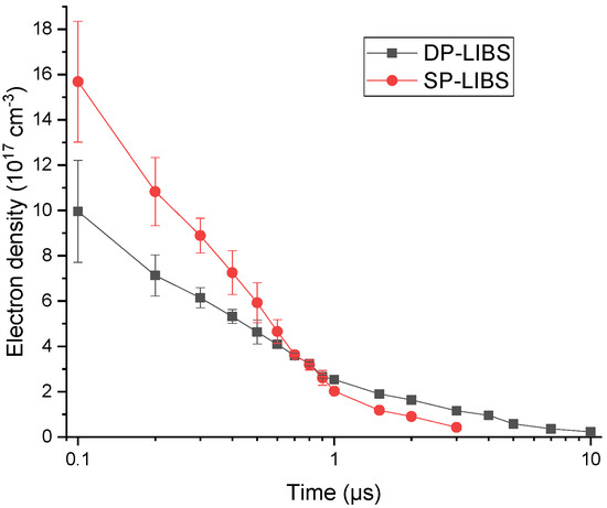
Figure 5.
Time-resolved evolution of the electron density, obtained from the Stark broadening for SP-LIBS and DP-LIBS experiments.
From Figure 5 it can be seen that, initially, the electron density obtained with SP-LIBS is somewhat higher compared to that obtained using DP-LIBS. This may be due to the fact that the second pulse is produced in a medium with a lower density. As a result, plasma expansion velocity is higher than if the breakdown occurred in undisturbed air. It should also be noted that the re-excitation pulse arrives 4 µs after ablation breakdown, so the electron density increases by about two orders of magnitude up to ~1018 cm−3. The mechanism that gives rise to the re-excitation using an infrared laser is mainly due to inverse Bremsstrahlung [53]. In addition, it has been reported that by using a longer wavelength, absorption is performed more efficiently [54]. This results in a larger enhancement of the ionic emission lines than of the neutral ones [53,54], in agreement with the findings displayed in Figure 3. It is also observed that after 1 µs, the calculated values for the DP-LIBS experiment are higher than those obtained with a single pulse. In addition, the emission of Cd and Te lines can be detected for three times longer than in the SP-LIBS configuration, which contributes to the observed emission enhancement. This can be attributed to the fact that the second pulse increases the total number of emitters [49].
The determination of the plasma temperature was performed using the multi-element Saha–Boltzmann plot. All spectroscopic data were taken from the NIST and Kurucz databases [55,56]. The employed transitions to make the plots were: 238.33 and 238.58 nm (Te I); 226.74, 230.66 and 232.93 nm (Cd I); 231.28 and 232.11 nm (Cd II). The obtained results are shown in Figure 6, where the error bars are obtained from the error in the slope when making the linear fit of the Saha–Boltzmann plots. As can be seen from the figure, when the second pulse is applied, the values achieved are similar to those initially obtained with a single pulse. The main difference is that the plasma temperature in the DP-LIBS configuration decayed much slower than the SP-LIBS scheme, similar to what was observed for the electron density. Thus, the temperature could be measured up to 10 µs, a value one order of magnitude higher than in the SP-LIBS case. This is possibly due to the fact that the second pulse forms a plasma with much higher energy and a larger volume; therefore, it remains excited for a longer time.
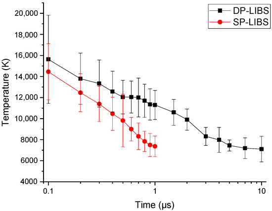
Figure 6.
Temporal evolution of plasma temperature, obtained from the multi-element Saha–Boltzmann method. For the DP-LIBS configuration, time zero is defined as the time at which re-excitation occurs.
3.3. Determination of Self-Absorption
As mentioned above, it is also necessary to verify that the lines employed to calculate the relative compositions are not self-absorbed. For this purpose, in addition to the spectroscopic parameters and the plasma temperature, the width of the spectral lines, the plasma length and the total density of species are also required. The width of the lines as a function of time was directly obtained from measured spectra. The plasma length l was determined from the shadowgrams. Thus, for instance, the plasma increases in size from less than 1 mm at 500 ns to 2.6 mm in width and 1.4 mm in height 4 µs after the ablation pulse.
Likewise, it is necessary to know the density of emitting species . This was calculated from the total number of removed particles from the target, assuming that all of them were atomized. For this purpose, the volume removed per pulse was measured via profilometry; the mass and number of removed particles were calculated from the target mass density. On the other hand, the plasma volume as a function of time was estimated from the shadowgrams, assuming a semi-ellipsoid shape for the ablation plasma. The ratio between the number of ablated particles and the plasma volume gives an estimate of the total density number (ions and neutrals) contained in the plasma. Finally, from the Saha equation [46], the number density of ions and neutrals, , was calculated. The proportion of ions and neutrals present in the plasma at a temperature T can also be obtained from the NIST-LIBS database [55]. The experimental results from the above calculation are shown in Figure 7. The 228.80 and 226.50 nm lines belonging to Cd I and Cd II, respectively, have low SA values, indicating that both lines are highly self-absorbed. For the neutral transition, the SA decreases with time since the percentage of neutrals increases by nearly two orders of magnitude as the plasma temperature drops from 1.3 to 0.6 eV. The other excited transitions presented a low or negligible self-absorption effect.
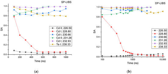
Figure 7.
Time-resolved evolution of self-absorption coefficient SA for selected Cd and Te transitions for (a) SP-LIBS and (b) DP-LIBS. Wavelengths are given in nanometers.
Moreover, an averaged SA value slightly higher for the double pulse experiment compared to the standard LIBS experiment was observed.
The integrated intensity of an optically thin line I0 could be written as a function of the emission intensity I as I0 = I/SA0.46, where SA is the self-absorption coefficient for the investigated line [44]. Thus, a value of 0.8 for SA, as was obtained for some transitions shown in Figure 7, corresponds to a difference in areas within 11%. This difference typically falls within the LIBS errors when measuring line intensities due to pulse-to-pulse variations. Hence all the excited transitions reported here could be safely employed to calculate the relative composition of films.
The above calculations were conducted using an estimated upper value for some of the parameters employed. For example, the plasma length l and volume were taken from SP-LIBS measurements. For DP-LIBS, both parameters may be larger, reducing the effect of self-absorption. This is due to the fact that, from the shadowgrams, it was not possible to differentiate the plasma produced in the air from that produced by ablation. For instance, the spectra acquired in the SP-LIBS configuration showed the self-reversal effect for the 228.8 and 226.50 nm transitions, which was not observed in DP-LIBS. This is also an indication that the DP-LIBS configuration contributed to the reduction in the self-absorption of the lines.
Finally, it should be noted that most of the parameters used in the calculation shown in Figure 7 have an error. For example, the error of the plasma volume calculation via shadowgraphy is up to 30% for 100 ns after plasma onset, reducing to 10% after 600 ns. Additionally, it is necessary to consider the error in the calculation of both the electron density and the plasma temperature. Thus, a SA value of 0.8 can be lowered to 0.7, but the effect on a transition with a value of 0.98 only decays to 0.97. In any case, it should be highlighted that all transitions used for the plasma temperature calculation have a low self-absorption, so they can be safely used for the calculation performed.
3.4. Relative Composition of Thin Films
For the determination of the relative composition of thin films, the certified CdTe target was employed as the reference sample; therefore, in Equation (2), N1r/N2r = 1. Then the intensities were obtained for both the thin films and the reference target by averaging 20 shots at different spots on the surface. With these data, sufficient statistics are generated to calculate a final value with an associated uncertainty obtained by error propagation. Thus, the relative composition was determined by considering the possible combinations between the Cd and Te lines. It was decided to only use the 238.33 nm Te I transition of tellurium. Its intensity was analytically obtained from the whole area of the doublet because the 600 l/mm grating does not resolve it clearly from the 238.58 nm line (see Figure 4); here, the intensity of the used transition is 1/3 of the total measured area. Other observed tellurium transitions, such as the 253.07 nm, overlapped with silicon transitions from the substrate, and the 225.91 nm could only be detected in the double pulse arrangement. From Figure 7, only three cadmium transitions were optically thin enough to perform the calculation, but we decided to add the Cd II 219.46 nm. This transition has the same configuration and term as 231.28 nm and a similar gkAkj value. The Cd II 214.44 nm resonant transition was ruled out due to its high gkAkj which makes it prone to self-absorption.
Then, by plotting the ratio I1α I2r/I1rI2α, the relative composition of cadmium to tellurium can be obtained. The obtained results from this procedure are shown in Figure 8 for two films grown on silicon and glass. The identified transitions were taken from the NIST and Kurucz databases [55,56]. Since, via X-ray diffraction analysis, only CdTe was found in the composition of the thin films, it follows that N1α = N2α. Consequently, the quotient shown in the figure should be one. When applying a double pulse, most of the calculated relative compositions tend to the expected theoretical value, whereas, for the single pulse configuration, there is a more marked divergence. The associated uncertainty for the compositions is slightly lower when DP-LIBS is applied compared to SP-LIBS. The averaged and error values (see the last bar of the figure) were calculated from the reported ratios in the figure for the different transitions.
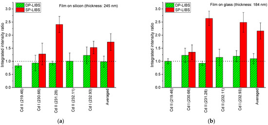
Figure 8.
Relative composition of the analyzed sample of CdTe grown on (a) a microstructured crystalline silicon substrate and (b) a glass substrate. Wavelengths are given in nanometers and the 238.33 nm from Te I was taken as reference.
As can be seen, the ratios obtained using the DP-LIBS configuration are much closer to the expected value than when using a single laser. This is possibly due to the low SNR in the SP-LIBS configuration. In addition, the use of a second pulse to increase the intensity of the emission lines has been found to reduce self-absorption, providing an effective method for determining the relative composition of thin films.
An interesting issue observed is that, by performing the ratios of other intense transitions in which the effect of self-absorption was observed, the ratio in both experimentally investigated schemes showed values close to one. This was performed for the three transitions that were previously discarded: 228.80 nm (Cd I), and 214.44 and 226.50 nm (Cd II). For example, the average ratio of these three lines for the SP-LIBS case is 1.24 with a standard deviation SD = 0.15, while for DP-LIBS, an average value of 0.93 with an SD = 0.05 was obtained. In fact, it is observed that the ratio obtained for SP-LIBS is closer to one than that of the value obtained using non-self-absorbed lines. This is possible because the former has a higher relative intensity than those shown in Figure 8. This is unexpected and possibly related to the fact that these lines are equally self-absorbed in both the films and the target used as a reference. Therefore, by performing the ratios, the correct relative composition is obtained.
4. Conclusions
In this work, orthogonal double-pulse LIBS in a reheating configuration was used to characterize the composition of CdTe thin films. To minimize damage to the films, an ablation energy of 0.5 mJ was employed, and this removed an approximately 25 µm diameter region of the thin films grown on silicon substrates. Using the double-pulse arrangement, a significant improvement in the signal-to-noise ratio was obtained for a wide range of inter-pulse delays. The enhancement obtained is mainly due to the increase in plasma temperature and a longer emission persistence. It was also found that the use of double-pulse LIBS, reduced the self-absorption of the emission lines. Therefore, the relative composition of the films is closer to the expected value than when using single-pulse LIBS. The results showed that even using self-absorbed transitions, it was possible to make a good estimate of the composition of the thin films. This may be related to the fact that this effect affects both the films and the target used as a reference.
Finally, the use of a double-pulse reheating configuration allowed us to determine the relative composition of thin films with reasonable accuracy. The analysis can be performed quickly in the same laboratory where the samples were grown without causing significant damage to the samples.
Author Contributions
G.Q.-S.: conceptualization, investigation, writing—original draft. H.S.: writing—review and editing, validation, supervision, J.R.-C.: materials preparation, investigation, methodology. All authors have read and agreed to the published version of the manuscript.
Funding
This work was supported by the National Autonomous University of Mexico (DGAPA-UNAM: IN104421).
Institutional Review Board Statement
Not applicable.
Informed Consent Statement
Not applicable.
Data Availability Statement
The data presented in this study are available on request from the corresponding author.
Acknowledgments
The authors are grateful to A. Robledo-Martinez for the critical reading of the manuscript.
Conflicts of Interest
The authors declare no conflict of interest.
References
- Manimozhi, T.; Ramamurthi, K.; Sinthiya, M.M.; Karthigeyan, A.; Bhuvanaswari, P.V.; Ramesh Babu, R. Effect of Substrate Temperature on the Properties of Nanocrystalline CdTe Thin Films Coated by Electron Beam Evaporation Method. Int. J. ChemTech Res. 2015, 7, 950–957. [Google Scholar]
- Bosio, A.; Pasini, S.; Romeo, N. The History of Photovoltaics with Emphasis on CdTe Solar Cells and Modules. Coatings 2020, 10, 344. [Google Scholar] [CrossRef]
- Romeo, A.; Artegiani, E. CdTe-Based Thin Film Solar Cells: Past, Present and Future. Energies 2021, 14, 1684. [Google Scholar] [CrossRef]
- Dharmadasa, I.M.; Echendu, O.K.; Fauzi, F.; Abdul-Manaf, N.A.; Olusola, O.I.; Salim, H.I.; Madugu, M.L.; Ojo, A.A. Improvement of Composition of CdTe Thin Films During Heat Treatment in the Presence of CdCl2. J. Mater Sci. Mater Electron. 2017, 28, 2343–2352. [Google Scholar] [CrossRef]
- Ling, J.; Zhang, X.; Mao, T.; Li, L.; Wang, S.; Cao, M.; Zhang, J.; Shi, H.; Huang, J.; Shen, Y.; et al. Electrodeposition of CdTe Thin Films for Solar Energy Water Splitting. Materials 2020, 13, 1536. [Google Scholar] [CrossRef]
- Gu, P.; Zhu, X.; Wu, H.; Yang, D. Regulation of Substrate-Target Distance on the Microstructural, Optical and Electrical Properties of CdTe Films by Magnetron Sputtering. Materials 2018, 11, 2496. [Google Scholar] [CrossRef]
- Arnold, C.B.; Aziz, M.J. Stoichiometry Issues in Pulsed-laser Deposition of Alloys Grown from Multicomponent Targets. Appl. Phys. A. 1999, 69, S23–S27. [Google Scholar] [CrossRef]
- Major, J.D. Grain Boundaries in CdTe Thin Film Solar Cells: A Review. Semicond. Sci. Technol. 2016, 31, 093001. [Google Scholar] [CrossRef]
- Chaudhary, K.; Rizvi, S.Z.H.; Ali, J. Laser-Induced Plasma and its Applications. In Plasma Science and Technology—Progress in Physical States and Chemical Reactions; Mieno, T., Ed.; IntechOpen: London, UK, 2016; Available online: https://www.intechopen.com/chapters/49562 (accessed on 14 September 2022).
- Richardson, M. Laser Produced Plasmas. In Experimental Methods in the Physical Sciences, 1st ed.; Samson, J.A.R., Ederer, D.L., Eds.; Academic Press: Cambridge, MA, USA, 1998; Volume 31, pp. 83–92. [Google Scholar]
- Afonso, C.; Gonzalo, J.; Sena, R.; Solis, J. Pulsed Laser Deposition for Functional Optical Films. In Laser Ablation and its Applications; Phipps, C., Ed.; Springer Science-Business Media: New York, NY, USA, 2007; pp. 315–338. [Google Scholar]
- Stafe, M.; Marcu, A.; Puscas, N.N. Pulsed Laser Ablation of Solids. Basics, Theory and Applications, 1st ed.; Springer: Berlin/Heidelberg, Germany, 2014; pp. 15–51. [Google Scholar]
- Legnaioli, S.; Lorenzetti, G.; Pardini, L.; Cavalcanti, G.H.; Palleschi, V. Applications of LIBS to the Analysis of Metals. In Laser-Induced Breakdown Spectroscopy Theory and Applications, 1st ed.; Musazzi, S., Perini, U., Eds.; Springer: Berlin/Heidelberg, Germany, 2014; Chap. 7; pp. 181–182. [Google Scholar]
- Hahn, D.W.; Omenetto, N. Laser-Induced Breakdown Spectroscopy (LIBS), Part II: Review of Instrumental and Methodological Approaches to Material Analysis and Applications to Different Fields. Appl. Spectrosc. 2012, 66, 347–419. [Google Scholar] [CrossRef]
- Noll, R. Laser-Induced Breakdown Spectroscopy, Fundamentals and Applications, 1st ed.; Springer: Berlin/Heidelberg, Germany, 2012; pp. 7–16. [Google Scholar]
- Li, W.; Li, X.; Li, X.; Hao, Z.; Lu, Y.; Zeng, X. A review of remote laser-induced breakdown spectroscopy. App. Spectrosc. Rev. 2020, 55, 1–25. [Google Scholar] [CrossRef]
- Jolivet, L.; Leprince, M.; Moncayo, S.; Sorbier, L.; Lienemann, C.P.; Motto-Ros, V. Review of the recent advances and applications of LIBS-based imaging. SAB 2019, 151, 41–53. [Google Scholar] [CrossRef]
- Noll, R.; Fricke-Begemann, C.; Connemann, S.; Meinhardt, C.; Sturm, V. LIBS analyses for industrial applications—An overview of developments from 2014 to 2018. J. Anal. At. Spectrom. 2018, 33, 945–956. [Google Scholar] [CrossRef]
- Singh, V.K.; Sharma, J.; Pathak, A.K.; Ghany, C.T.; Gondal, M.A. Laser-induced breakdown spectroscopy (LIBS): A novel technology for identifying microbes causing infectious diseases. Biophys. Rev. 2018, 10, 1221–1239. [Google Scholar] [CrossRef] [PubMed]
- Wu, J.; Qiu, Y.; Li, X.; Yu, H.; Zhang, Z.; Qiu, A. Progress of laser-induced breakdown spectroscopy in nuclear industry applications. J. Phys. D Appl. Phys. 2020, 53, 1–24. [Google Scholar] [CrossRef]
- Liu, C.; Ling, Z.; Zhang, J.; Wu, Z.; Bai, H.; Liu, Y. A Stand-Off Laser-Induced Breakdown Spectroscopy (LIBS) System Applicable for Martian Rocks Studies. Remote Sens. 2021, 13, 4773. [Google Scholar] [CrossRef]
- Papazoglou, D.G.; Papadakis, V.; Anglos, D. In situ interferometric depth and topography monitoring in LIBS elemental profiling of multi-layer structures. J. Anal. At. Spectrom. 2004, 19, 483–488. [Google Scholar] [CrossRef]
- Dwivedi, V.; Marín-Roldán, A.; Karhunen, J.; Paris, P.; Jõgi, I.; Porosnicu, C.; Lungu, C.P.; van der Meiden, H.; Hakola, A.; Veis, P. CF-LIBS quantification and depth profile analysis of Be coating mixed layers. Nucl. Mater. Energy 2021, 27, 100990. [Google Scholar] [CrossRef]
- Canel, T.; Demir, P.; Kacar, E.; Genc Oztoprak, B.; Akman, E.; Gunes, M.; Demir, A. Optimization of parameters for depth resolution of galvanized steel by LIBS technique. Opt. Laser Technol. 2013, 54, 257–264. [Google Scholar] [CrossRef]
- De Bonis, A.; De Filippo, B.; Galasso, A.; Santagata, A.; Smaldone, A.; Teghil, R. Comparison of the performances of nanosecond and femtosecond Laser Induced Breakdown Spectroscopy for depth profiling of an artificially corroded bronze. App. Surf. Sci. 2014, 302, 275–279. [Google Scholar] [CrossRef]
- Sobral, H.; Amador-Mejía, M.; Márquez-Herrera, C. Characterization of Pottery from Teotihuacan by Laser-Induced Breakdown Spectroscopy and Inductively Coupled Plasma-Optical Emission Spectroscopy. Appl. Spectrosc. 2021, 75, 728–738. [Google Scholar] [CrossRef]
- Aragón, C.; Madurga, V.; Aguilera, J.A. Application of laser-induced breakdown spectroscopy to the analysis of the composition of thin films produced by pulsed laser deposition. Appl. Surf. Sci. 2002, 197, 217–223. [Google Scholar] [CrossRef]
- Pender, J.; Pearman, B.; Scaffidi, J.; Goode, S.R.; Michael Angel, S. Laser-induced breakdown spectroscopy using sequential laser pulses. In Laser-Induced Breakdown Spectroscopy (LIBS): Fundamental and Applications, 1st ed.; Miziolek, A.W., Palleschi, V., Schechter, I., Eds.; Cambridge University Press: Cambridge, UK, 2006. [Google Scholar]
- Tognoni, E.; Cristoforetti, G. Signal and noise in Laser Induced Breakdown Spectroscopy: An introductory review. Opt. Laser Technol. 2016, 79, 164–172. [Google Scholar] [CrossRef]
- Li, Y.; Ding, Y.; Yang, G.; Liu, K.; Wanch, C.; Han, X. A review of laser-induced breakdown spectroscopy signal enhancement. Appl. Spectr. Rev. 2018, 53, 1–35. [Google Scholar] [CrossRef]
- Sanginés, R.; Contreras, V.; Sobral, H.; Robledo-Martinez, A. Optimal emission enhancement in orthogonal double-pulse laser-induced breakdown spectroscopy. Spectrochim. Acta Part B 2015, 110, 139–145. [Google Scholar] [CrossRef]
- Popescu, A.C.; Beldjilali, S.; Socol, G.; Craciun, V.; Mihailescu, I.N.; Hermann, J. Analysis of indium zinc oxide thin films by laser-induced breakdown spectroscopy. J. Appl. Phys. 2011, 110, 083116. [Google Scholar] [CrossRef]
- Acquaviva, S.; D’Ann, E.; De Giorgi, M.L.; Moro, F. Laser-induced breakdown spectroscopy for compositional analysis of multielemental thin films. Spectrochim. Acta Part B 2006, 61, 810–816. [Google Scholar] [CrossRef]
- Davari, S.A.; Hu, S.; Pamuac, R.; Mukherjee, D. Calibration-free quantitative analysis of thin-film oxide layers in semiconductors using laser induced breakdown spectroscopy (LIBS). J. Anal. At. Spectrom 2017, 32, 1378–1387. [Google Scholar] [CrossRef]
- Caneve, L.; Colao, F.; Sarto, F.; Spizzichino, V.; Vadrucci, M. Laser-induced breakdown spectroscopy as a diagnostic tool for thin films elemental composition. Spectrochim. Acta Part B 2005, 60, 1098–1102. [Google Scholar] [CrossRef]
- Hermann, J.; Axente, E.; Pelascini, F.; Craciun, V. Analysis of Multi-Elemental Thin Films via Calibration-Free Laser-Induced Breakdown Spectroscopy. Anal. Chem. 2019, 91, 2544–2550. [Google Scholar] [CrossRef]
- Lee, S.H.; Shim, H.S.; Kim, C.K.; Yoo, J.H.; Russo, R.E.; Jeong, S. Analysis of the absorption layer of CIGS solar cell by laser-induced breakdown spectroscopy. Appl. Opt. 2012, 51, B115–B120. [Google Scholar] [CrossRef]
- Banerjee, P.; Sarneta, T.; Siozosb, P.; Loulakisb, M.; Anglosb, D.; Sentis, M. Characterization of organic photovoltaic devices using femtosecond laser induced breakdown spectroscopy. Appl. Surf. Sci. 2017, 418, 542–547. [Google Scholar] [CrossRef]
- Owens, T.; Mao, S.S.; Canfield, E.K.; Grigoropoulos, C.P.; Mao, X.; Russo, R.E. Ultrafast thin-film laser-induced breakdown spectroscopy of doped oxides. Appl. Opt. 2010, 49, C67–C69. [Google Scholar] [CrossRef]
- Nishijima, D.; Hollmann, E.M.; Doerner, R.P. Spatially-offset double-pulse laser-induced breakdown spectroscopy: A novel technique for analysis of thin deposited layers. Spectrochim. Acta Part B 2016, 124, 82–86. [Google Scholar] [CrossRef]
- Sanginés, R.; Sobral, H. Time Resolved Study of the Emission Enhancement Mechanisms in Orthogonal Double-Pulse Laser-Induced Breakdown Spectroscopy. Spectrochim. Acta B 2013, 88, 150–155. [Google Scholar] [CrossRef]
- Harilal, S.S.; Phillips, M.C.; Froula, D.H.; Anoop, K.J.; Isaac, R.C.; Beg, F.N. Optical Diagnostics of Laser-Produced Plasmas. Rev. Mod. Phys. 2022, 94, 035002. [Google Scholar] [CrossRef]
- Rangel-Cárdenas, J.; Sobral, H. Optical Absorption Enhancement in CdTe Thin Films by Microstructuration of the Silicon Substrate. MDPI Materials 2017, 10, 607. [Google Scholar] [CrossRef]
- Bredice, F.O.; Di Rocco, H.O.; Sobral, H.M.; Villagrán-Muniz, M.; Palleschi, V.A. new method for determination of self-absorption coefficients of emission lines in Laser-Induced Breakdown Spectroscopy experiments. Appl. Spectrosc. 2010, 64, 320–323. [Google Scholar] [CrossRef]
- El Sherbini, A.M.; El Sherbini, T.; Hegazy, H.; Cristoforetti, G.; Legnaioli, S.; Pardini, L.; Palleschi, V.; Salvetti, A.; Tognoni, E. Measurement of the Stark Broadening of Atomic Emission Lines in Non–Optically Thin Plasmas by Laser-Induced Breakdown Spectroscopy. Spectrosc. Lett. 2007, 40, 643–658. [Google Scholar] [CrossRef]
- Aguilera, J.A.; Aragón, C. Multi-element Saha–Boltzmann and Boltzmann plots in laser-induced plasmas. Spectrochim. Acta Part B 2007, 62, 378–385. [Google Scholar] [CrossRef]
- Gautier, C.; Fichet, P.; Menut, D.; Lacour, J.L.; L’Hermite, D.; Dubessy, J. Quantification of the intensity enhancements for the double-pulse laser-induced breakdown spectroscopy in the orthogonal beam geometry. Spectrochim. Acta Part B 2005, 60, 265–276. [Google Scholar] [CrossRef]
- Gautier, C.; Fichet, P.; Menut, D.; Lacour, J.L.; L’Hermite, D.; Dubessy, J. Study of the double-pulse setup with an orthogonal beam geometry for laser-induced breakdown spectroscopy. Spectrochim. Acta Part B 2004, 59, 975–986. [Google Scholar] [CrossRef]
- Tognoni, E.; Cristoforetti, G. Basic mechanism of signal enhancement in ns double-pulse laser-induced breakdown spectroscopy in a gas environment. J. Anal. At. Spectrom. 2014, 29, 1318–1338. [Google Scholar] [CrossRef]
- Konjevic, N.; Lesage, A.; Fuhr, J.R.; Wiese, W.L. Experimental Stark Widths and Shifts for Spectral Lines of Neutral and Ionized Atoms (A Critical Review of Selected Data for the Period 1989 Through 2000). J. Phys. Chem. Ref. Data 2002, 31, 819–927. [Google Scholar] [CrossRef]
- Simic, Z.; Dimitrijevic, M.S.; Kovacevic, A. Stark broadening of spectral lines in chemically peculiar stars: Te I lines and recent calculations for trace elements. New Astron. Rev. 2009, 53, 246–251. [Google Scholar] [CrossRef]
- El Sherbini, A.M.; Hegazy, H.; El Sherbini, T.M. Measurement of electron density utilizing the Hα-line from laser produced plasma in air. Spectrochim. Acta Part B 2006, 61, 532–539. [Google Scholar] [CrossRef]
- Scaffidi, J.; Angel, S.M.; Cremers, D. A Emission Enhancement Mechanisms in Dual-Pulse LIBS. Anal Chem. 2006, 78, 24–32. [Google Scholar] [CrossRef]
- St-Onge, L.; Detalle, V.; Sabsabi, M. Enhanced Laser-Induced Breakdown Spectroscopy Using the Combination of Fourth-Harmonic and Fundamental Nd:YAG Laser Pulses. Spectrochim Acta B 2002, 57, 121–135. [Google Scholar] [CrossRef]
- NIST Atomic Spectra Database Lines Form. National Institute of Standards and Technology. Available online: https://www.nist.gov/pml/atomic-spectra-database (accessed on 15 October 2022).
- Atomic Spectral Line Database from CD-ROM 23 of R.L. Kurucz. Available online: https://lweb.cfa.harvard.edu/amp/ampdata/kurucz23/sekur.html (accessed on 15 October 2022).
Disclaimer/Publisher’s Note: The statements, opinions and data contained in all publications are solely those of the individual author(s) and contributor(s) and not of MDPI and/or the editor(s). MDPI and/or the editor(s) disclaim responsibility for any injury to people or property resulting from any ideas, methods, instructions or products referred to in the content. |
© 2022 by the authors. Licensee MDPI, Basel, Switzerland. This article is an open access article distributed under the terms and conditions of the Creative Commons Attribution (CC BY) license (https://creativecommons.org/licenses/by/4.0/).