1. Introduction
As one of the seven basic units of the International System of Units, temperature has a crucial role in measuring physical quantities. It is necessary to measure and control temperature in our production life. In the industrial field, accurate control of smelting temperature in the steel smelting process can significantly improve product quality [
1,
2]. In the medical field, for pathological observation requires accurate measurement of human body temperature in real-time. In the use of some therapeutic methods such as magnetic resonance imaging, and thermal hysteresis therapy, the physical parameters of the equipment used need to be adjusted by temperature indicators. A suitable temperature environment is also required for raw material production, pharmaceutical water production, formulation production, powder/solid drug synthesis, drug sterilization, and drug preservation. The observation of temperature deviations, fluctuations, etc., can also be used to monitor the status of drugs, and blood [
3,
4,
5,
6,
7,
8,
9,
10,
11]. In the electromechanical field, for auxiliary facilities such as power generation mainframe equipment, engine propellers, and hydraulic oil, accurate temperature measurements are required to monitor the operation of the system and thus ensure the proper operation of the project [
12,
13,
14,
15].
Nowadays, with the development of technology intelligence, integration, and miniaturization, thin-film thermocouples based on Micro-Nano manufacturing technology are gradually taking the dominant position with the advantages of small size, lightweight, low power consumption, high reliability, high sensitivity, easy integration, and resistance to the harsh working environment [
16,
17,
18,
19]. In 2011, Varrenti demonstrated a 50 nm thick chromium-nickel thin-film thermocouple on a semiconductor substrate with a thin-film thermocouple with a Seebeck coefficient calibrated to 10.37 μV/°C. The measurable temperature range is 20 °C to 160 °C. The thermal accuracy of the integrated system can be less than 1 °C and shows good repeatability of the Seebeck coefficient. However, the repeatability of the sensor was not tested [
20]. In 2017, for the problem of high-temperature transient measurement on the instrument surface in the fields of hypersonic vehicles and round-trip vehicles between heaven and earth, Li prepared a thin-film thermocouple with a much smaller specific heat capacity than ordinary thermocouples and an effective fit to the product surface based on K-type thermocouples. The sensor can measure transient high temperatures up to 800 °C with a maximum measurement error of less than ±4 °C and a response time of less than 50 ms for thin-film thermocouples [
21]. In 2022, Luo prepared a zinc-rich Al-doped ZnO/indium tin oxide thin film thermocouple. The Seebeck coefficient of the thermocouple was kept constant at 168 μV/°C between 50 °C to 500 °C. The calculated errors of the sensor were less than 1% over this temperature range and were calibrated three times, showing good repeatability [
22]. In 2022, Cui used the magnetron sputtering technique for temperature measurement of rolling elements of bearings during vehicle operation, and deposited alumina thin films, NiCr thin films, NiSi thin films, and silica thin films on an aluminum alloy substrate successively. The fabricated thin film thermocouple has good linearity in the temperature range of 30~180 °C. The nonlinear fitting error of the sensor is less than 0.29% and the repeatability error is less than 4.55% [
23].
In this work, a high-precision three-dimensional probe array temperature sensor is designed with rapid response, high accuracy, small size, and easy integration. The temperature measurement range of the sensor is −60~200 °C, the temperature drift rate is 0.0626 °C/min, the repeatability error is 0.12%, the maximum hysteresis is 1.01%, and the accuracy can be improved to ±0.19%FS by the accuracy correction algorithm. The prepared high-precision probe type sensor has great application prospects in hydraulic systems, medical testing, and other fields.
2. Simulation and Fabrication
On the one hand, Metal and alloy were excellent thermoelectric materials due to their high thermal conductivity and mature processing technology. On the other hand, for the miniaturization of a three-dimensional probe array temperature sensor, thermoelectric materials with compensating wires can be a better choice. The copper and constantan are selected as the thermo-electrodes materials of the sensor because of the good linearity and stability of electromotive force (EMF) in low-temperature environment. The equivalent plane structure of electrodes is shown in
Figure 1a. Especially, a constantan negative electrode and three copper positive electrodes consisted of an array structure with three independent hot junctions (J1–J3). In order to analyze the feasibility and thermo-electric property of the designed structure, the finite element analysis software is used for the simulation. The key physical parameters are listed in
Table 1 for the simulation of a three-dimensional probe array temperature sensor.
The temperature of J1 is set from −60 °C to 100 °C while a temperature gradient of 50 °C existing between J1~J3 and the temperature of cold junctions kept 20 °C as shown in
Figure 1b.
Figure 1c shows the result of static thermo-electric simulation, which shows a potential distribution with a gradient similar to the temperature distribution. There is a constant EMF difference between J1~J3, which means every junction could sense an independent temperature difference. In
Figure 1d–f, the same temperature is applied to the three temperature junctions. The simulation results show that the three sensors have a good consistency. In the uniform temperature field of the region, three temperature junctions can greatly increase the testing accuracy and reliability of the sensor.
Figure 2 shows the section diagram and the schematic of the three-dimensional probe array temperature sensor. Polyetheretherketone (PEEK) has high-temperature resistance, superior mechanical properties, and excellent chemical resistance, which was selected as the substrate of the probe array temperature sensor. In particular, its electrical insulation makes a transition layer between the base material and the thermal electrode layer unnecessary. As shown in
Figure 2a, the geometry of the substrate is designed as a cylinder with a diameter of 4 mm and a length of 15 mm. At the same time, there are four radial rectangular grooves where the electrode film is deposited on arrayed circumferentially on the surface of the cylinder. Moreover, the end of the cylinder had a taper which is beneficial for axial fixation of the substrate in the assembly structure shown in
Figure 2b. In
Figure 2b, conductive silver paste was used to connect compensation wires (copper wires and constantan wire) and thermocouple legs. With the help of the retaining ring, the main body of the probe array temperature sensor was packaged in a hexagon-headed bolt. The standardized threaded connection of this simple package structure made the installation of the sensor more flexible.
The process flow of the probe array temperature sensor is shown in
Figure 3. Briefly, by using a photoresist and a special shadow mask of hot junctions, the copper electrode was deposited onto the PEEK substrate which had been cleaned with acetone and anhydrous ethanol with ultrasonic cleaning for 20 min. The constantan electrode was fabricated in the same way. After that, epoxy resin was coated on rectangular grooves as the protective layer. Moreover, owing to the low thermal conductivity of epoxy resin (0.5 W·m
−1·K
−1), SiC (83.6 W·m
−1·K
−1) was chosen to deposit onto the hot junctions of the sensor.
Table 2 shows the process parameters of the three-dimensional probe array temperature sensor. The prepared sample is shown in
Figure 3.
3. Testing and Process Optimization
Heat treatment is a common method to modify thin films [
10,
12,
24]. In this work, based on the process preparation parameters in
Table 2, heat treatment of the prepared film was carried out at different time and temperature parameters. Combined with the actual working conditions and the characteristics of the thin film, the sensor characteristics under different heat treatment parameters are compared by annealing for 1/2/3 h at 200/250/300 °C. Nine groups of film thermocouple samples with different heat treatments were tested by a static calibration system, including sensor sensitivity, temperature time drift rate, repeatability error, hysteresis, and full range error, etc.
In this work, a high-accuracy calibration system as shown in
Figure 4 was built for a wide temperature range. The prepared sensor was calibrated in a high and low-temperature chamber (FWD701P) with an accuracy of ±0.3 °C. Different from previous work the A grade three-wire type pt1000 with an accuracy of ±0.15 °C was selected as the measuring standard instrument for the temperature of the hot and cold end [
24,
25]. To reduce the temperature non-uniformity between pt1000 and cold end, the sensor’s cold end was settled in the water bath by the T-type compensation wires. The EMF of the sensor and resistance change of pt1000 were recorded with a data acquisition system (Keithley Instruments DMM6500, KEITHLEY, Shanghai, China).
The working principle of the three-dimensional probe array temperature sensor is based on the Seebeck effect, which describes the thermo-diffusion of charge carriers as a function of the temperature. When a closed loop consisted of two different conductors exposed to a temperature gradient, the voltage generated between the two ends is a function of the temperature. The sensitivity of the sensor can be calculated by Equation (1):
S is the sensitivity coefficient of the sensor; ΔV is the EMF and ΔT is the temperature difference between the hot (Th) and the cold end (Tc).
The temperature drift of the sensor can describe the temperature stability, which can be calculated by Equation (2).
where
DR(T) is the temperature drift rate, Δ
V(T) refers to the maximum interpolation of the output EMF for the holding time of the sensor,
T is the maintained temperature, Δ
t stands for holding time (10 min) and
V(T)ref is the reference voltage.
The repeatability error of thermocouples can be calculated by Equation (3) as follows:
The is repeatability error, Smax is the maximum standard deviation and YFS is the full-scale output.
Output characteristic parameters of sensors with different heat treatment parameters are shown in
Table 3. It is obvious from the test and calculation results that all parameters of the sensor have been improved comprehensively after heat treatment. However, in terms of accuracy, this parameter is not improved after heat treatment. This is because the accuracy is affected by many aspects, not only post-processing, but also the film preparation process parameters and the equipment itself. From the heat treatment results in
Table 3, it was found that the sensor treated at 250 °C for 3 h had the best comprehensive characteristics. After heat treatment, the temperature-time drift rate, repeatability error, and hysteresis of the thin-film thermocouple were significantly reduced (57.16~73.68%), while the full-scale accuracy and sensitivity of the sensor did not change significantly. This is because the accuracy and sensitivity are influenced by many factors in addition to the heat treatment process, such as film thickness and deposition quality, compared to the temperature-time drift rate, repeatability error, and hysteresis of the thin-film thermocouple.
The analysis of the electron transport mechanism of metal thin films shows that the heat treatment process can change the microscopic crystal organization of metal thin films and reduce the internal defects, thus changing their carrier mobility and affecting the thermoelectric properties. To investigate the mechanism of the influence of the heat treatment process on the microscopic morphology of thin films, scanning electron microscopy (SEM) and X-ray diffractometer (XRD) are used in this section to examine the microscopic morphology and organization of thin film samples after different heat treatments.
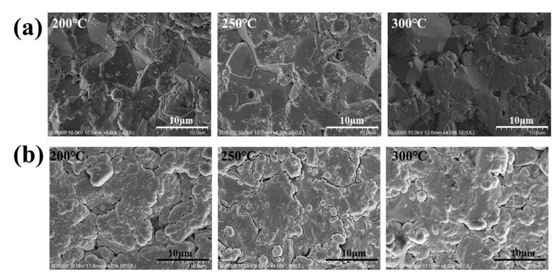
To investigate the effect of heat treatment temperature on the microscopic morphology organization of the films, the prepared thin film thermocouple samples were heat treated in a nitrogen atmosphere for 1 hour and the heat treatment temperature was varied.
Figure 5 shows the SEM micromorphology of the Cu and CuNi thin films when the heat treatment temperature was changed. With the increase of heat treatment temperature, the particle size of Cu thin film tissue gradually increases, the particle boundary decreases and the surface densities of the films increase significantly.
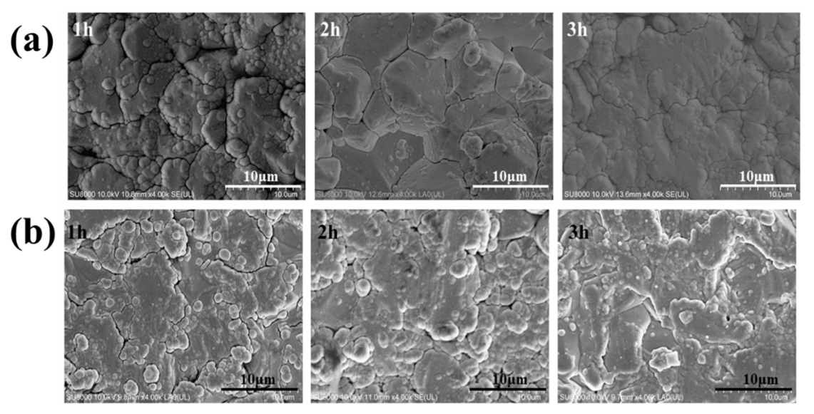
To investigate the effect of heat treatment time on the microscopic morphological organization of the films, the prepared thin film thermocouple samples were subjected to heat treatment at 250 °C in a nitrogen atmosphere and the heat treatment time was varied.
Figure 6 shows the SEM micromorphology of the Cu and CuNi films when the heat treatment time was varied. With the increase of heat treatment time, the particle size of thin film tissue gradually increases, the particle boundary decreases, the surface densities of the films are significantly increased, and the surface flatness increases.
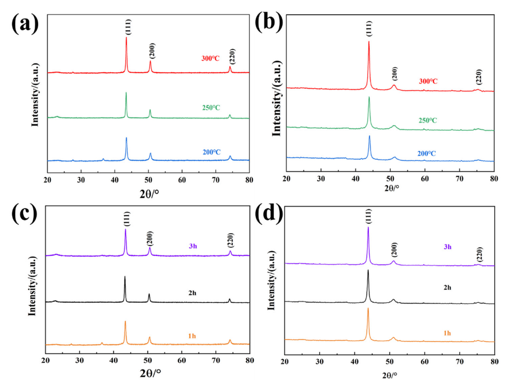
To prevent the oxidation of the films due to the high heat treatment temperature, the maximum heat treatment temperature is only 300 °C. Therefore, the surface morphological changes of the films are not obvious in SEM images. To further investigate the grain structure of the films affected by the heat treatment process, XRD is used to analyze the physical phase of the film samples.
The XRD patterns of Cu and CuNi films at different heat treatment temperatures are shown in
Figure 7. The intensity of each diffraction peak of Cu and CuNi thin films increases significantly with the increase of heat treatment temperature, among which the intensity of (111) and (200) diffraction peaks increases significantly with the heat treatment temperature, which proves that the film tissues are recrystallized on this crystal plane. To measure the degree of recrystallization, the average grain size can be calculated by Scherrer’s equation. The average grain size of CuNi film is smaller than that of Cu film, which is consistent with the SEM figure. With the increase of heat treatment temperature, the grain size of Cu and CuNi films also increases, which proves that high temperature causes recrystallization of the films, leading to the continuous increase of grain size. The increase in grain size leads to a decrease in the number of grains per unit volume, and the decrease of grain boundary reduces the scattering effect on carriers, and the resistivity of the film decreases, thus stabilizing and enhancing the thermoelectric properties of the film. From
Figure 7, it can be calculated that after annealing at 250 °C for 1 to 3 h, the grain size of Cu and CuNi films grows from 26.1 nm to 42.2 nm and from 15.4 nm to 19.4 nm, respectively.
4. Precision Optimization
To make a connection between the output characteristic of thermoelectricity and temperature difference, the sensor’s cold end was kept at 23 °C in the water bath and the hot were heated from −60 °C to 100 °C with a rate of 5 °C/min. The output characteristic curves of three junctions of thermocouples by using the calibration system were shown in
Figure 8. The curves of “Temperature–EMF” of three junctions of the sensor are shown. From the data in
Figure 8a, it is apparent that the output characteristic curves of three junctions exhibit high consistency even if on the curved substrate. Moreover, the maximum and minimum of the sensor are 3.19 mV and −3.22 mV, and the sensitivity of the sensor is about 40.1 μV/°C. Besides, the temperature resolution of three junctions is guaranteed to be less than 0.1 °C.
What can be clearly seen in
Figure 8a is the non-ideal linearity of the actual output curve of the sensor, which is due to the changes of the Seebeck coefficient of electrodes at different temperatures. Therefore, the second polynomials are better to fit the thermoelectric voltage output curves, which are given as Equation (4):
where
E is EMF whose unit is mV, and Δ
T is the temperature difference whose unit is °C. According to the collected data, the coefficients of thermoelectric voltage output curves of three junctions were calculated in
Table 4.
What stands out in
Table 4 is the ultra-high coefficients of determination (R
2 > 0.9999) which can accurately reflect the fitting degree between the model and the actual EMF. The R
2 close to 1 means that a more accurate temperature value could be calculated by the thermoelectric voltage fitting curves. However, the coefficients (A and C) of J3 are quite different from that of J1 and J2. It is believed that this is due to the influence of the inhomogeneity of film on the curve substrate.
To assess the repeatability error and temperature drift of the sensor, the repeated cycles of heating, holding, and cooling the hot end shown in
Figure 8b were carried out. Specifically, the temperature in the chamber went up from −60 °C to 100 °C for five repeated cycles and remained stable at −60 °C, 20 °C, and 99 °C for 30 min in the first cycle.
Table 5 shows the results of the drift rate of three junctions at three different temperatures. The maximum temperature drift rate of the three junctions are 0.0470 °C/min, 0.0626 °C/min and −0.0329 °C/min, which show great temperature stability. Each junction of the sensor shows the character of high reliability. The foundation is set for the sensor to ensure the monitoring of temperature in the actual measurement. The repeatability error calculated in
Figure 8b is 0.12%.
The full-scale error calculation of the prepared multi-junction type thin film thermocouple is shown in
Figure 9a. From the analysis of the figure, it is shown that among the three junctions, the maximum full-scale error of the output thermal potential of junctions J1 and J2 is less than ±0.5%FS, which is much smaller than the full-scale error of junction J3 (>±1.0%FS). This is due to the lower consistency of the deposited film process on the curved surface compared to the flat surface, resulting in a larger error profile for J3 compared to the other two junctions. The analysis also revealed that the prepared multi-junction sensor had different error magnitudes for each junction at different temperature bands. For example, in the range of 20~60 °C, the error of junction J1 is obviously smaller than the other two junctions, while in the range of 80~120 °C, the error of junction J2 is obviously smaller than J1 and J3. Based on this characteristic, an accuracy calibration method based on the redundant structure of multiple junctions is developed.
The schematic diagram of the multi-junction accuracy calibration method is shown in
Figure 10, which is similar to the piecewise fitting method. The three junctions are respectively fitted with thermoelectric curves, and the thermoelectric curves obtained from the fitting are
E1(Δ
t),
E2(Δ
t), and
E3(Δ
t). At the same time, the accuracy test is carried out according to the thermoelectric curve obtained by fitting, and the full-scale error curve shown in the figure is obtained. Then divide the full scale into three temperature sections, and the boundary values of the sections are
t0~
t3 respectively, and compare the maximum errors of the three junctions in each temperature section, and take the thermoelectric curve of the junction where the smallest is located as the temperature range. The output curve of the thin film thermocouple. For example, in the temperature range
t0~
t1, the maximum measurement error of the J1 is the smallest, so in this temperature range,
E−1(Δ
t) is used as the output curve of the thin film thermocouple. Similarly, within
t1~
t2, the maximum measurement error of the J2 is the smallest, and
E−1(Δ
t) is used as the output curve of the thin film thermocouple. Then the full-scale output curve of the thermocouple is finally obtained as:
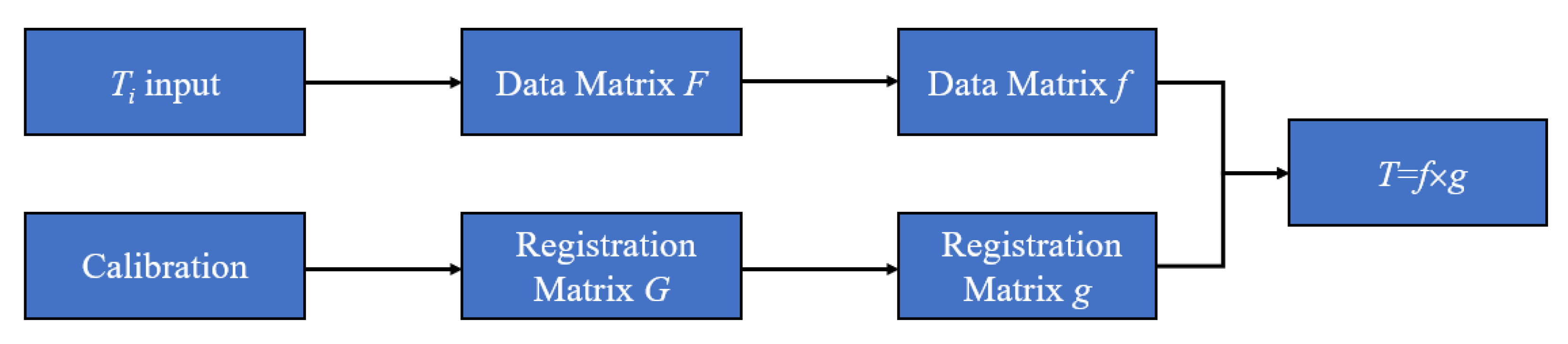
The Data registration procedures shown in
Figure 11 can be divided into the following three steps:
Step 1: After accuracy calibration and measurements of temperature to be measured, the original data matrix
F and registration matrix
G are marked as follows:
where
T1~
T3 are the measured value calculated by Equation (7) of the temperature
T, and
is their average value.
where the matrix
G is the registration matrix, which is got from the calibrations of the fabricated sensor. Where
ti stand for a median of a certain temperature intervals when the measurement range of the sensor is divided into several isometric temperature intervals. The
αij is the coefficient of the accuracy of junction
Ji in the temperature interval of [(3
ti −
ti+1)/2, (
ti +
ti+1)/2]. Meanwhile, in this temperature interval, the value of
αij for the
Ji which has a minimum measurement error is 1, and the other two are 0.
Step 2: By comparing the difference between
and
ti, the temperature interval including the temperature
T can be determined. For example, when
takes 26 °C,
ti takes 25~195 °C with a gradient of 10 °C, and the temperature intervals including the temperature
T can be determined as [20, 30]. Then, the submatrices,
f and
g respectively belonging to
F and
G are generated, which can be derived as follows:
Step 3: The temperature
T can be calculated as the following equation:
Figure 9a shows the full range error curve of the thin film thermocouple after accuracy calibration, when the divided temperature interval length is 20 °C, the maximum full range error of the sensor is more than ±1.0%FS in the range of −60~200 °C. We can reduce the length of the divided interval for accuracy calibration, and obtain the maximum full-scale error of the sensor under different interval lengths, as shown in
Figure 9b. With the reduction of the divided temperature interval lengths, the maximum full-scale error of the thin film thermocouple is significantly reduced, and when the temperature interval length is 1 °C, the maximum full-scale error is only 0.19%. Based on the calculated results, the prepared high-precision three-dimensional probe array temperature sensor has a temperature deviation of 0.494 °C in the range of −60 °C to 200 °C. According to the existing standards for the development of industrial thermocouples, the sensors achieve Class I accuracy (GB/T 30429-2013).


 ,
, 


