Article

In2O3 Based Hybrid Materials: Interplay between Microstructure, Photoelectrical and Light Activated NO2 Sensor Properties

1
Chemistry Department, Moscow State University, 119991 Moscow, Russia
2
Faculty of Materials Science, Moscow State University, 119991 Moscow, Russia
3
A.N. Nesmeyanov Institute of Organoelement Compounds RAS, 119991 Moscow, Russia
4
Quantum Technology Center, Moscow State University, 119991 Moscow, Russia
5
Faculty of Physics, Moscow State University, 119991 Moscow, Russia
*
Author to whom correspondence should be addressed.
Chemosensors 2022, 10(4), 135; https://doi.org/10.3390/chemosensors10040135
Submission received: 28 February 2022 / Revised: 30 March 2022 / Accepted: 1 April 2022 / Published: 4 April 2022
(This article belongs to the Special Issue Functionalized Materials for Chemosensor Applications)

Abstract

:
In this work, organic–inorganic hybrids based on nanocrystalline indium oxide and ruthenium (II) heteroleptic complexes were used as sensitive materials for room temperature light-activated NO2 detection. In2O3 was obtained by chemical precipitation method and then annealed at three different temperatures (T = 300, 500, 700 °C) in order to investigate the influence of the microstructure of indium oxide on sensor characteristics of hybrid materials and on kinetics of the rise and fall of photoconductivity. The results of the X-ray phase analysis demonstrated that the obtained materials are single-phase with a cubic bixbyite structure. The Ru (II) heteroleptic complex, which was used as a photosensitizer, made it possible to shift the optical sensitivity range of the hybrids to the low energy region of the spectrum and to use a low-power LED (λmax = 470 nm) source for the photoactivation process. The sensor properties were investigated toward NO2 at sub-ppm range at room temperature. It was found that for pure oxides, the sensor signal correlates with a specific surface area, while for hybrid materials, both the sensor signal and photoresponse increase with increasing the matrix crystallinity. In this case, the main role is played by traps of nonequilibrium charge carriers, which are structural defects in the matrix.

1. Introduction

Since the early 2000s, organic–inorganic hybrid materials have become a rapidly developing investigation objects and attract special attention within the framework of fundamental research and industrial application in the field of gas sensors [1,2,3,4]. This is due to the fact that such systems can have new or improved physicochemical functional properties through a synergistic interaction between the constituent components in the interface. In this regard, organic dyes and QD (quantum dots) as photosensitizers are of particular interest as the receptor part of the system, which allow shifting the optical sensitivity of wide-gap semiconductor oxides towards lower energies due to their high extinction coefficient in the visible region of the spectrum [5,6,7,8,9,10]. The location of HOMO and LUMO levels allows one to control the generation of photoexcited charge carriers and their transfer to the semiconductor conduction band [11,12,13,14,15,16], while the composition (central cation and ligands) and structure (chirality and steric effects) of the complex itself can contribute to additional and specific interaction with gas phase molecules [17,18,19].
However, there are pitfalls in the form of physical and chemical parameters of materials, such as composition and microstructure that can either limit or facilitate their use as gas sensors [20,21,22,23,24].
Previously, the authors of the works [25,26] already carried out a study of the influence of the In2O3 microstructure on the NO2 detection. It was concluded that the dependence of the sensor signal on the size of nanocrystals is nonmonotonical; it is connected with the concentration and mobility of the electrons and was explained on the basis of the potential barriers on the boundary of nanocrystals. However, the influence of the matrix microstructure in hybrid systems, where the photosensitizer provides the transfer of charge carriers, still remains unexplored.
The possibility of using the organic–inorganic hybrid materials based on nanocrystalline SnO2 or In2O3 and Ru(II) heteroleptic complexes for the efficient photoactivated detection of nitrogen oxides (NO2 and NO) at room temperature was published in our earlier works [8,9,27]. A recent study of a series of Ru(II) complexes based on 1H-imidazo [4,5-f][1,10] phenanthroline derivatives (ImPh) demonstrated that the complex with the bithiophene ligand demonstrates the most effective photosensitization effect [16]. At the same time, the NO and NO2 gas sensor properties of hybrids based on In2O3 turned out to be two orders of magnitude higher than that of SnO2, which may be due to a smaller band gap and higher number of nonequilibrium charge carriers of the first one [8,9].
Based on the background experience, we have focused our attention in this work on the study of the influence of the In2O3 microstructure on the NO2 detection in sub-ppm range at room temperature by hybrid materials with the Ru(II) heteroleptic complex as the photosensitizer. Particular consideration is paid to the photoelectrical properties of the obtained materials.

2. Materials and Methods

2.1. Materials Synthesis

2.1.1. Synthesis of Nanocrystalline In2O3

The synthesis of nanocrystalline In2O3 was carried out by deposition of an aqueous solution of indium (III) chloride with ammonia solution followed by heat treatment. A solution of NH3·H2O (1 M) was added dropwise into a water solution of InCl3·4H2O (3.5 M) with vigorous stirring until pH ~ 6 was reached. The synthesis was carried out at room temperature. The following reaction took place:
2InCl3 + 6NH3·H2O + (x − 3)H2O → In2O3·xH2O ↓ + 6NH4Cl
The formed dense gel-like precipitate was separated by centrifugation, then it was washed with deionized water, and with 0.01 M NH4NO3 solution after the beginning of peptization until the chloride ions were removed. An opalescence absence was verified by adding a AgNO3 solution (0.01 M). Next, the In2O3·xH2O gel was dried at 50 °C for 24 h. The resulting glassy mass was grounded to a powder state in an agate mortar and annealed in air at three different temperatures (T = 300, 500 and 700 °C) for 24 h.

2.1.2. The Heteroleptic Ru(II) Complex as Photosensitizer

A detailed description of the synthesis method of heteroleptic Ru(II) complex is given in Supplementary Materials. Table 1 shows the structural formula, the energies of HOMO and LUMO and the label of the complex in this work.

2.1.3. Synthesis of Hybrid Materials

Organic–inorganic hybrid materials were obtained both in the form of powders for the composition and optical characterization and in the form of thick films to study the photoelectric and sensor properties. The sensitization of indium oxide in the form of a powder was carried out by the impregnation method; thick films of pure oxides were formed on microelectronic hotplates and then the solution of the heteroleptic Ru(II) complex was directly deposited dropwise on their surface. The concentration of the solution was chosen so that the total content of [Ru] relative to [In] was 0.5 wt%. The microelectronic hotplate consists of a metal base with leads, in the center of which a dielectric substrate made of Al2O3 (0.9 × 0.9 × 0.25 mm) is fixed on with platinum wires (Figure 1). The substrate is covered with Pt electrodes (0.18 mm in width) on the top side for resistance measurements and a Pt heater (0.18 mm in width) on the back side.
Figure 1d,e shows the side view and top view SEM images of the sensitive layer deposited on the substrate, respectively. As the sensitive layer is deposited from a suspension with α-terpineol, the surface dries unevenly; this explains why the surface has a wavy shape with an average thickness of 110 ± 10 μm. The surface of the thick film after annealing in the flow of dry air at T = 300 °C during 3 h is porous and consists of agglomerated and sintered grains. The size of agglomerates is about 50–80 nm.

2.2. Materials Characterization

The phase composition of the obtained In2O3 was investigated by X-ray diffraction on a DRON-4-07 diffractometer (radiation source—CuKα with λ = 1.5418 Ǻ). The phase composition was determined using the STOE WinXPOW software. The ICDD PDF database was used to identify the peaks. The crystallite size (dXRD) was calculated using the Scherrer equation. The crystal structure of the synthesized samples was also studied by Raman spectroscopy. The studies were carried out on an i-Raman Plus spectrometer (BW Tek, Newark, Delaware, USA) equipped with a BAC 151C microscope. Raman spectra were recorded in the range of 90–2000 cm−1 with 4 cm−1 resolution; a laser with a wavelength of 532 nm was used as a radiation source. The thickness and morphology of the films were studied by scanning electron microscope (SEM) using a Carl Zeiss SUPRA 40 FE-SEM instrument (Carl Zeiss AG, Oberkochen, Germany) with Inlens SE detector. The specific surface area (Ssurf) of nanocrystalline oxides was measured by low-temperature nitrogen adsorption using a Chemisorb 2750 instrument (Micromeritics). The surface area available for adsorption was calculated using the BET model (Brunauer, Emmett, Teller). Oxidation centers on the surface of the synthesized materials were investigated by the thermo-programmed hydrogen reduction (TPR-H2) method, and also on a Chemisorb 2750 instrument (Micromeritics, Norcross, GA, USA) in a quartz reactor using a 10% H2/Ar gas mixture (50 mL/min) under heating up to 900 °C with 10 K/min rate.
Fourier Transform Infrared (FTIR) spectroscopy measurements were performed on a Spectrum One (Perkin Elmer Inc., Beaconsfield, UK) spectrometer in the transmission mode in the wavenumber range of 400–4000 cm−1 with a step of 1 cm−1. Samples (about 5 mg) were ground with 50 mg of potassium bromide (Aldrich, for FTIR analysis) and pressed into tablets 0.5 mm thick and 6 mm in diameter.
X-ray fluorescence analysis (XRF) was used to determine the elemental composition of hybrid materials. The study was performed on a M1 Mistral spectrometer (Bruker) with a tube voltage of 50 kV. The diameter of the analyzed region was 1.5 mm; the signal accumulation time was 1 min. The absorption spectra of semiconductor oxides and hybrid materials were obtained on a Perkin-Elmer Lambda-950 spectrophotometer in the diffuse reflection mode in the range of 200–800 nm with a step of 1 nm. The measurements of spectral dependence of the photoconductivity were studied in the range of 350–700 nm and were performed by using a halogen lamp as a white light source and MDR-206 monochromator to obtain irradiation with narrow spectral band. The illumination time for each wavelength was 1 min, and then followed by a stage of the material’s conductivity recovery to the initial stationary value at dark conditions. The conductivity of the samples was measured by a Keithley 6517A electrometer. The following equation was used to calculate the photoconductivity:
Δ σ σ 0 = σ ( λ ) σ 0 σ 0
where σ(λ)—is the conductivity of the thick film after 1 min of illumination with the corresponding wavelength; σ0—is the conductivity of the thick film in stationary state in dark conditions.
The gas sensor properties of hybrid materials were investigated by measuring the electrical conductivity of thick films in situ in a flow cell under a controlled gas flow of 100 ± 0.1 mL/min. The gas mixture for measurements was prepared by dilution with dry synthetic air using RRG-12 electronic mass-flow controllers. Sensor measurements were carried out at room temperature under conditions of periodic illumination with a blue light-emitting diode (LED, 8 mW/cm2, λmax = 470 nm, OTdiode, Shenzhen, China) located at a distance of 4 cm above the sensors.

3. Results and Discussion

3.1. Characteristics of Nanocrystalline In2O3

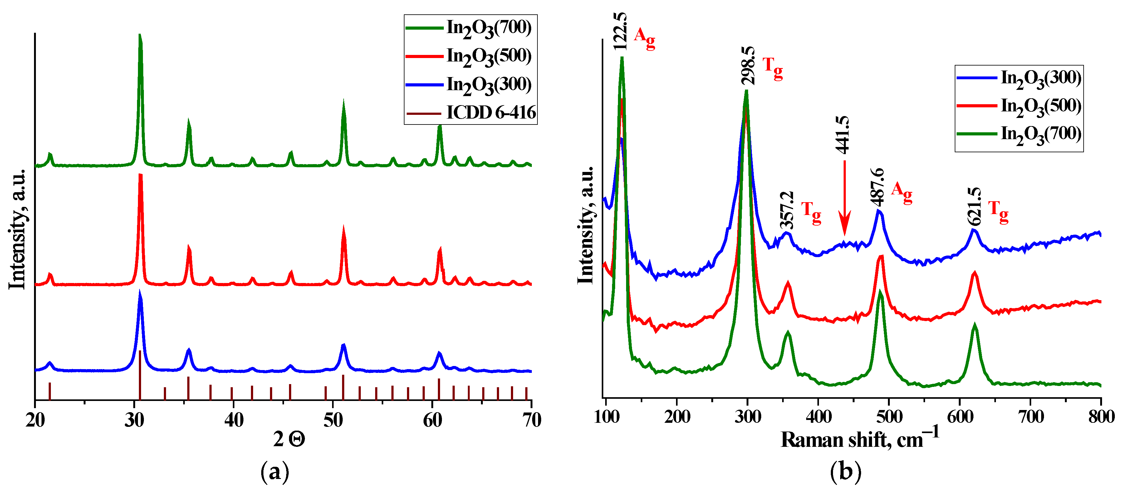
Figure 2a shows X-ray diffraction patterns of nanocrystalline In2O3 samples annealed at temperatures of 300, 500 and 700 °C. According to the results of X-ray phase analysis and ICDD PDF-2 database, the obtained indium oxide powders are single-phase corresponding to a cubic bixbyite structure. It was found that increasing the annealing temperature leads to an increase in crystallite size (dXRD) and a decrease in specific surface area (Ssurf) (Table 2).
Figure 2b represents the Raman spectra of nanocrystalline In2O3 samples annealed at temperatures of 300, 500 and 700 °C. The main characteristic Raman modes for the body-centered cubic lattice of In2O3 were observed. The peak at 122.5 cm−1 is associated with the vibrations of the In-O bond of the [InO6], and the peaks at 298.5 cm−1, 487.6 and 621.5 cm−1 are due to the deformation and stretching vibration of the [InO6] octahedrons, respectively. The stretching vibrations of In-O-In bonds were corresponded at 357.2 cm−1 [28,29,30]. However, the In2O3(300) sample contains a broad band at 441.5 cm−1, which corresponds to a superposition of surface modes. These vibration modes are characteristic of nanosized powders and indicate a highly defective surface layer [31]. It should also be noted that with an increase in the annealing temperature, the background of the Raman spectra descends and becomes horizontal. The defect structure leads to luminescence of the sample under the influence of a powerful radiation source, which leads to the rise in the baseline at higher values of the Raman shift. This statement confirms the defect structure of the surface of the samples annealed at lower temperatures.
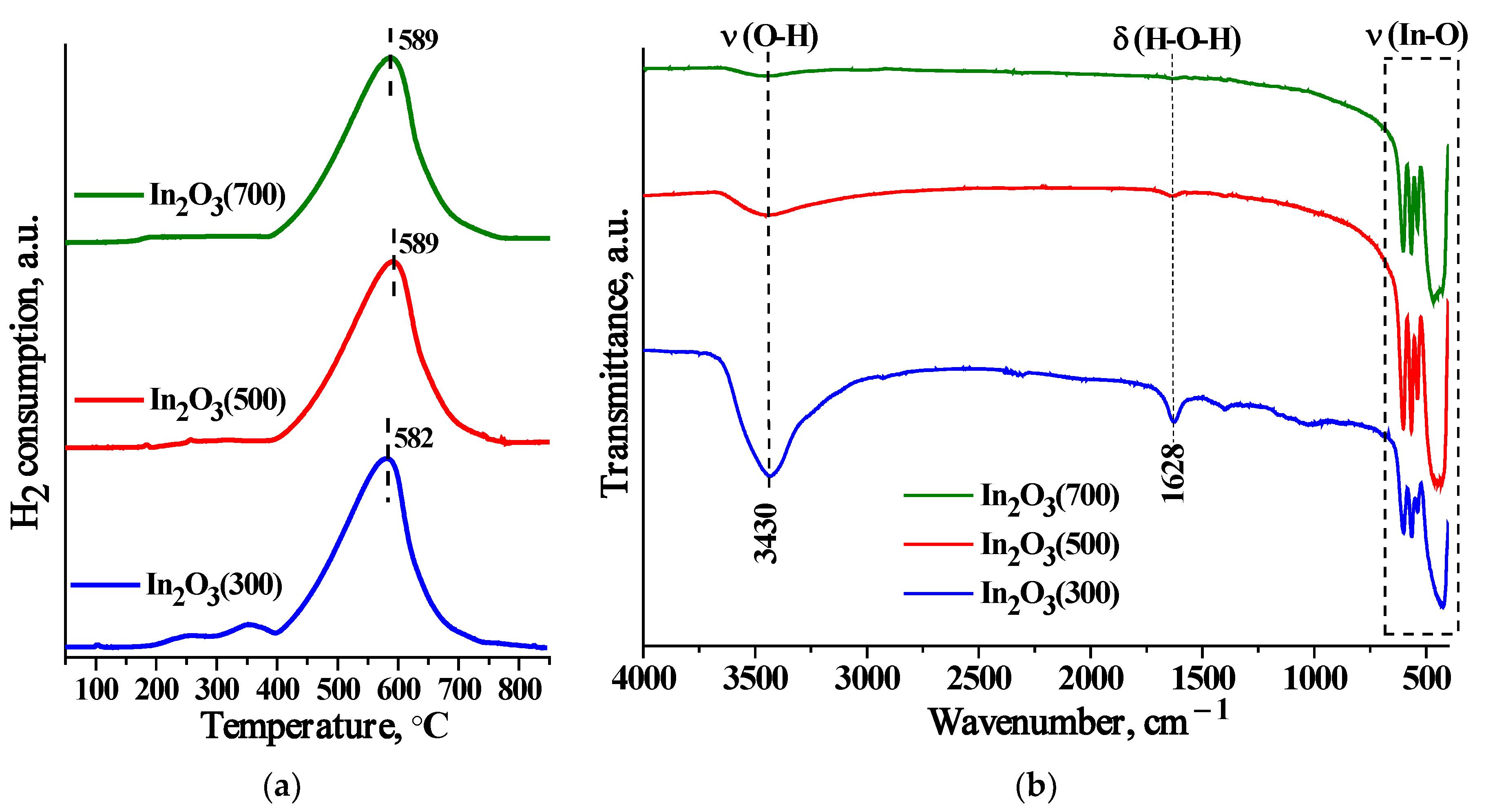
The curves of the TPR-H2 method are represented in Figure 3a. Two regions of hydrogen consumption can be distinguished—low-temperature (up to 400 °C) and high-temperature (above 400 °C). The absorption of hydrogen at low temperatures is due to the reduction of surface OH groups and various forms of chemisorbed oxygen:
OH(ads) + ½H2 = H2O
O2(ads) + 2H2 → 2H2O
In the high-temperature region, the H2 consumption is due to the reduction of In2O3 to metallic indium:
In2O3 + 3H2 → 2In + 3H2O
The amount of consumed hydrogen was calculated from the peak area, and the calibration was performed using a standard Ag2O sample. The calculation results of the H2 consumption for two temperature ranges are presented in Table 3. In the low-temperature region, the amount of absorbed hydrogen is 2 times higher in the case of the most dispersed sample (In2O3(300)), which indicates a greater number of surface OH groups and chemisorbed O2. A shift in the maximum H2 consumption peak and an increase in its amount with an increase in the annealing temperature of the sample can be observed in the high-temperature region. This is associated with an increase in the particle size and crystallinity degree of In2O3, which increases the crystal lattice energy, and therefore its destruction during bulk reduction requires large amounts of thermal energy. The total amount of hydrogen consumed during the reduction of In2O3 ranges from n = 3.0 to 3.3 mol of H2 per mol of In2O3, which is in good agreement with the theoretical value (n = 3 mol) of the reduction of indium oxide to metal (reaction (5)).
FTIR spectra of the samples are shown in Figure 3b. The spectra contain peaks corresponding to the vibrations of bonds in the crystal lattice of In-O (400–600 cm−1), adsorbed water (1628 cm−1) and hydroxyl groups (3000–3670 cm−1). With an increase in the annealing temperature, a decrease in OH groups on the surface is observed, while the In2O3(300) sample contains the largest number of OH groups, which is in good agreement with the TPR-H2 results.
The electrophysical properties of the In2O3(300), In2O3(500) and In2O
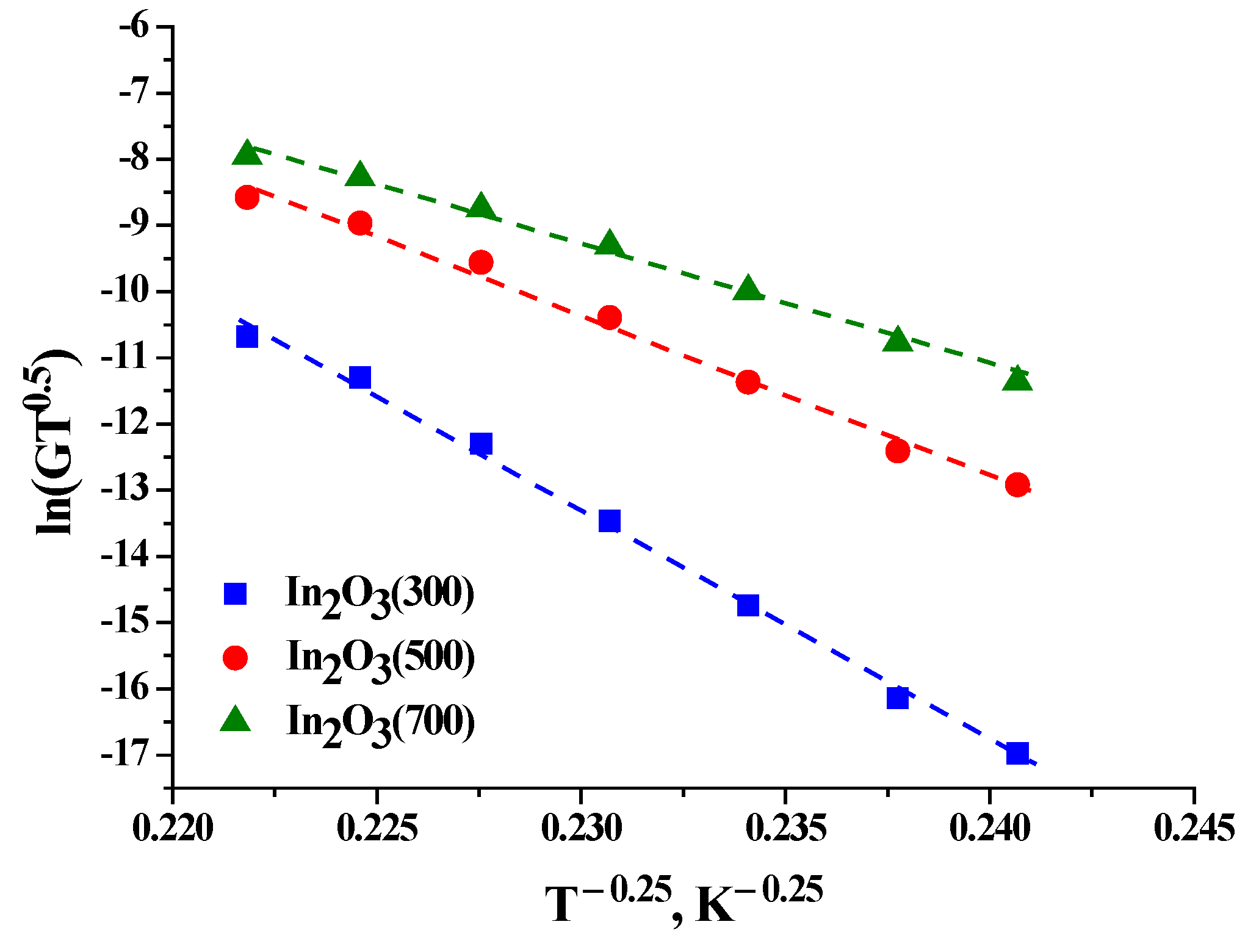
3(700) samples were investigated in the temperature range of 300–25 °C in a dry air flow. The temperature dependence of the conductivity has a complicated form for all samples, which may be associated with the chemisorption of oxygen from air. Therefore, in order to study the electrophysical properties, the temperature dependence of the conductivity was plotted in the Mott coordinates [32] (6):
G = G M T 0.5 e x p [ ( T M T ) 0.25 ]
where GM and TM are the Mott characteristic parameters.
This dependence is well linearized in the temperature range of 140–25 °C. The value of TM was calculated from the slope of the straight line ln(GT0.5) = f(T−0.25) (Figure 4). Then, using equations (7–9), the following characteristic parameters were calculated: N(EF), Rhop and Whop, where N(EF) is the density of localized states near the Fermi level, Rhop is the electron “jump” length, Whop is the “jump” energy electron, α is a quantity that describes the spatial degree of localization of the wave function, and is equal to 1.24 nm−1 and kB is the Boltzmann constant.
T M = 16 α 3 k B N ( E F )
R h o p = ( 9 8 π α k B T N ( E F ) ) 0.25
W h o p = 3 4 π R h o p 3 N ( E F )
Table 4 shows the parameters characterizing the conductivity of the studied samples according to the Mott model [32]. The Mott model assumes the activation character of conductivity, which indicates the presence of barriers, and the height of the barrier is directly proportional to the resistance of the material. In this case, the resistance value correlates with the grain size in the range of In2O3(300) > In2O3(500) > In2O3(700). The calculated values of the electron “jump” energy or activation energy (Whop) for the temperature range of 25–140 °C also changes monotonically, and may be associated with an increase in the crystallite size, which leads both to a decrease in the height of intergrain barriers and to a shift of the Fermi level to the edge of the conduction band.

3.2. Characteristics of Hybrid Materials

The results of a quantitative analysis of the composition of hybrid materials obtained by X-ray fluorescence analysis (XRF) are presented in Table 5. It can be observed from the table that the ruthenium content in the hybrids is close to the theoretically specified value [Ru]/([Ru] + [In]) = 0.5 wt.%. These values are averaged and taken from 4 different areas of the sample.
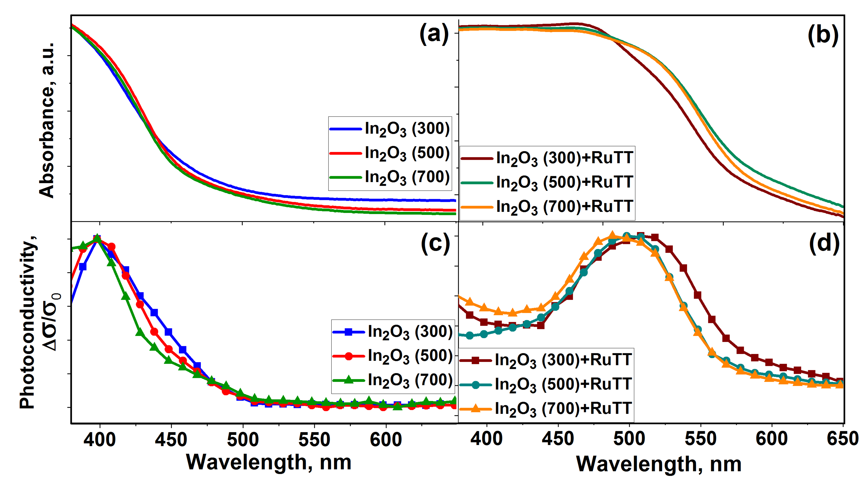
The optical absorption spectra (a,b) and normalized spectral dependences of the photoconductivity (c,d) of the sensitized composites and pure In2O3 samples are shown in Figure 5.
As can be observed from the figures, unmodified In2O3-based samples are transparent in the visible spectral range. All spectra exhibit an absorption band in the UV region, which corresponds to a direct transition from the valence band to the conduction band, as the energy of this transition exceeds the semiconductor band gap. The curves of the absorption spectra coincide and are overlapped on the curves of the spectral dependence of the photoconductivity for all samples. However, some features can be noticed. In particular, in Figure 5c, a shoulder is observed in the blue region of the spectrum, while its intensity increases with a decrease in the size of indium oxide crystallites. This may be related to excitation of the impurities within the bandgap, because the In2O3(300) sample has a more defective structure.
An absorption edge is observed in the visible region of the spectrum in hybrid materials due to the presence of organic complexes in their composition. Moreover, the maximum of the absorption edge for In2O3(500)+RuTT and In2O3(700)+RuTT samples is shifted to longer wavelengths by about 10 nm; for these composites, a bathochromic shift is observed. This shift may be associated with the stabilization effect of the excited states of Ru(II) heteroleptic complexes by the solid phase of the semiconductor oxide. The increase in photoconductivity for hybrid materials in the visible range of the spectrum indicates the transfer of photoexcited electrons from the Ru(II) heteroleptic complex to the conduction band of the semiconductor oxide.
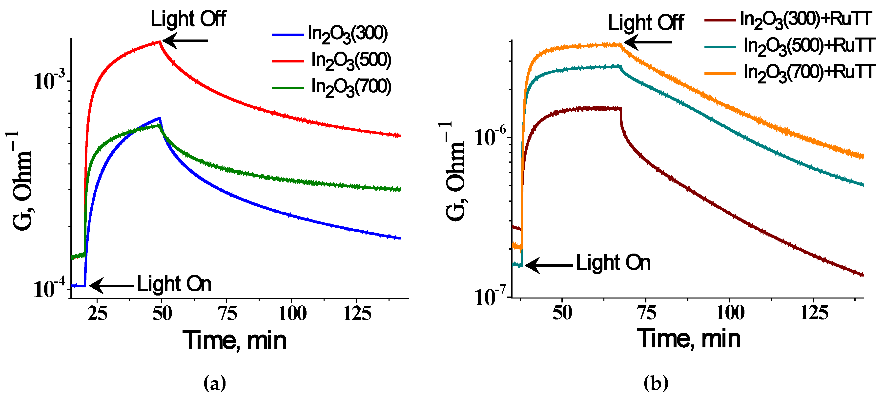
The photoconductivity of nanocrystalline In2O3 and hybrid materials was studied under constant illumination with blue LED (λmax = 470 nm). The curves of changes in the conductivity of the studied samples under illumination are shown in Figure 6. When the light is turned on, the electrical conductivity of materials increases; turning off the LED leads to relaxation of the conductivity. The effect of the annealing temperature of In2O3 on the behavior of photoconductivity under the influence of blue LED radiation is nonmonotonic. The maximum value of the photoresponse, calculated as the ratio of the conductivity under illumination to the conductivity under dark conditions, was achieved by the In2O3(500) sample. In this case, the change in conductivity can be associated with the presence of acceptor levels in the band gap of the semiconductor, as the value of the quantum energy corresponding to the emission of a blue LED is less than the band gap of indium oxide.
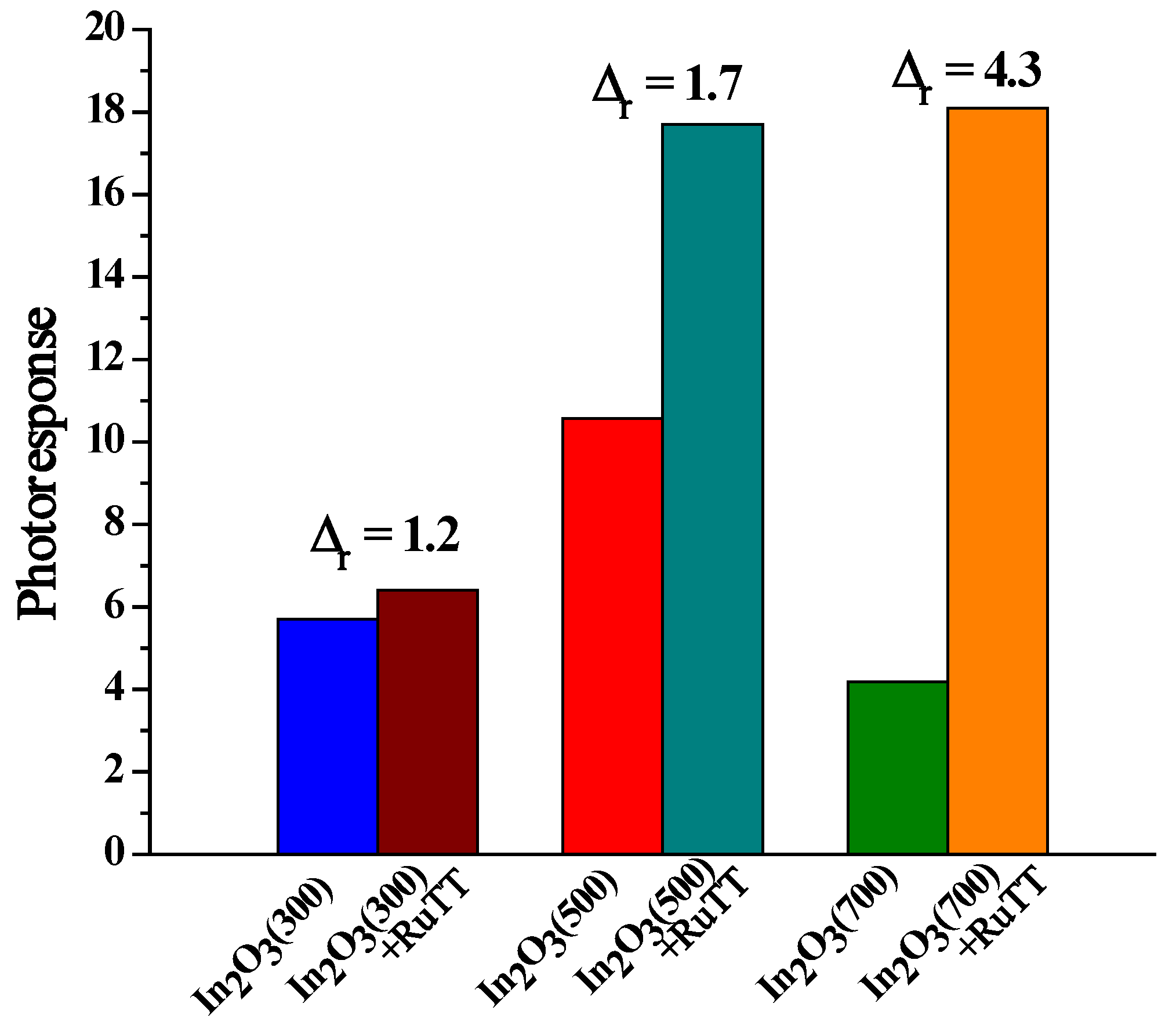
As can be observed, the difference in photoresponse between the hybrid material and the corresponding matrix increases with the increasing annealing temperature (Figure 7). The In2O3 annealed at 300 °C has the largest number of structural defects that can act as charge carrier traps. An increase in the annealing temperature leads to ordering of the system and structural perfection, leading to a decrease in the concentration of traps.

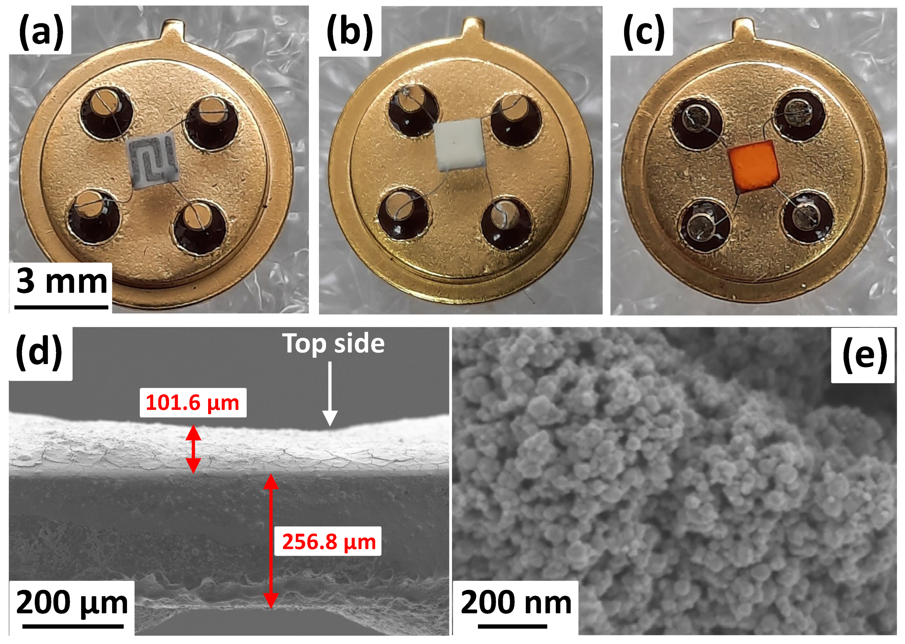
3.3. Investigation of the Gas Sensor Properties of Hybrid Materials in Interaction with Nitrogen Dioxide in Dry Air

The illumination of the sensor was carried out in a pulsed mode with periods of 2 min by switching on and off the LED, as a result of which the change in the resistance of the sensor with time also acquires a periodic character and is an alternation of the curves of the decay and rise of the photoconductivity. The repeated cycle of turning on and off the light leads to the change in the resistance of the sensor in each of the subsequent cycles close to the previous one. In this steady state, the minimum resistance Rlight is achieved during the illumination of the sensor and the maximum resistance Rdark is achieved in the dark conditions. The ratio (10) varies with the composition of the atmosphere and has been used as a “sensor signal” for this measurement technique.
S = R d a r k ( g a s ) R d a r k ( a i r )
S p h = R d a r k R l i g h t
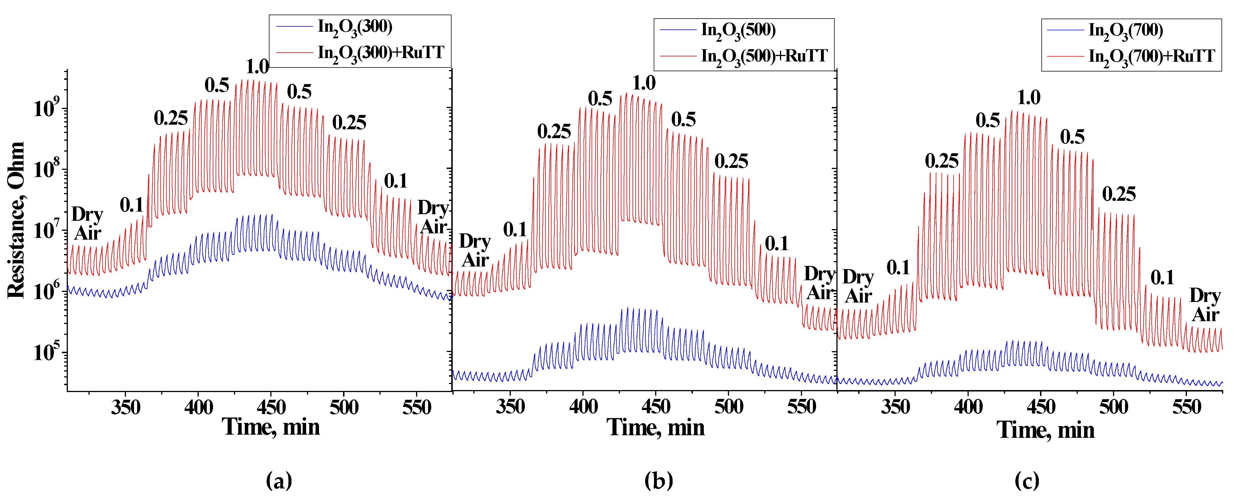
Figure 8 shows the change in the resistance of sensors based on pure oxides and hybrid materials under periodic blue LED illumination in the presence of various concentrations of NO2 (0.1–0.25–0.5–1.0 ppm). As can be observed, the sensors show a periodic change in resistance under the influence of pulsed illumination, both in air and in the presence of NO2. On the logarithmic scale of resistance, it can be observed that with an increase in the concentration of NO2, the ratio of the photoresponse (11) increases for all sensors sensitized with Ru(II) heteroleptic complex. Moreover, with an increase in the concentration of NO2, the average resistance of the sensors increases. The sensor resistances at the same NO2 concentrations, obtained both with an increase and a decrease in the detected gas in air, are very close, which indicates a good ability of these sensors to operate reversibly.
Table 6 represents the average values of the sensor resistances under dark conditions and constant light illumination in dry air. The resistances were measured during 1 h for each step, in order to obtain a relatively stable state. The first observation is that the resistance of all sensors under the LED illumination is much less, which is due to the photodesorption of oxygen from the surface that was adsorbed in the air flow in dark conditions. It can also be noticed that the higher the annealing temperature of the sample (resulting in larger In2O3 grain size), the lower the baseline resistance during measurements. This can be associated with the height of potential barriers at the grain boundary: the smaller the crystallite size, the higher the barrier.
In our previous works, it was demonstrated that the energy of the blue LED (λmax = 470 nm) excitation is equal to the absorption band of the Ru(II) heteroleptic complex in the visible range of the spectrum [8,9]. During light-activation, the electron-hole pairs are generated in it and then electrons can be transferred to the In2O3 conduction band facilitating to increase conductivity. NO2 being a stronger electron acceptor than O2, can attract the electrons from the conduction band of the semiconductor:
NO 2 ( gas ) + e NO 2 ( ads )
NO 2 ( gas ) + O 2 ( ads ) NO 2 ( ads ) + O 2 ( gas )
On the other hand, the chemisorbed particles (both NO 2 ( ads )   and   O 2 ( ads ) ) can be converted into physically sorbed particles by interaction with photogenerated holes:
NO 2 ( ads ) + h + NO 2 ( gas )
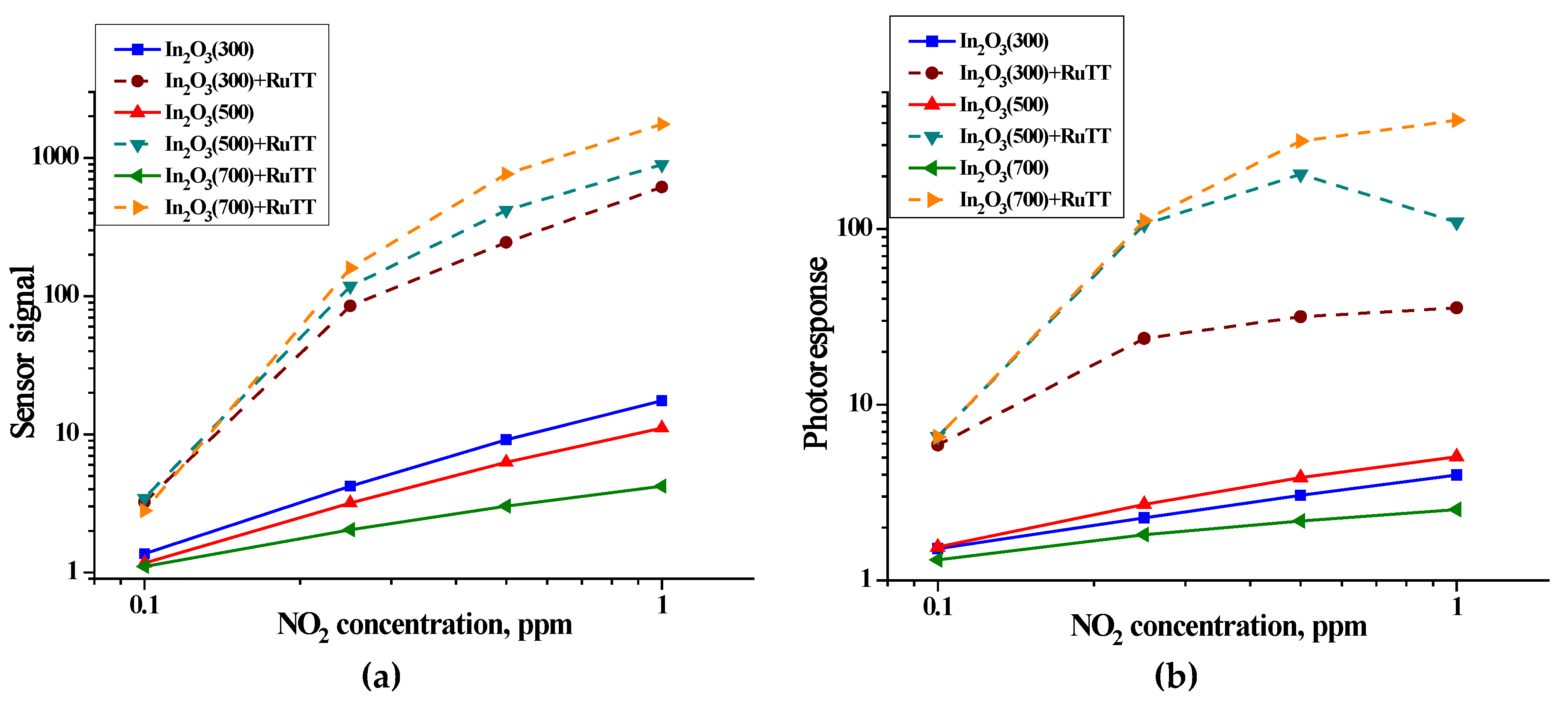
The values of the sensor signal were calculated using formula (10) and the photoresponse—using formula (11). The concentration dependences of the sensor signal and photoresponse of semiconductor oxides and hybrids are shown in Figure 9.
The obtained data show that the introduction of a photosensitizer into nanocrystalline oxides, In2O3, leads to an increase in sensor signal and photoresponse by 2–3 orders. For pure oxides, the sensor signal correlates with a specific surface area and is inversed with crystallite size. For hybrid materials, both the sensor signal and photoresponse increase with increasing matrix crystallinity. In this case, the main role is played by traps of nonequilibrium charge carriers, which are structural defects in the matrix. An increase in the annealing temperature decreases their concentration, which makes it possible to accelerate the kinetics of photoconductivity.
On the one hand, nanocrystalline In2O3 has a significant advantage over the sample with a large crystallite size, because nanosized crystalline grains have a large specific surface area, which leads to a more intense interaction of the semiconductor with the gas phase and, as a result, to an increase in the sensor signal. This was observed for pure oxides in NO2 detection. However, a consequence of a decrease in nanocrystals is an increase in the height of potential barriers at the grain boundary, which in turn can lead to a decrease in the mobility of free electrons and the probability of their tunneling [25,26]. The consequence of this was an increase in resistance with a decrease in the size of crystallites (Figure 8 and Table 6). The obtained result corresponds to the calculated values of the activation energy (Whop) for the samples at room temperature: In2O3(300) (0.55 eV) > In2O3(500) (0.38 eV) > In2O3(700) (0.29 eV). On the other hand, the crystal structure of nanosized materials is more defective, and that has been proven above using various characterization methods. Acting as traps, these defects can reduce the number of nonequilibrium charge carriers and, as a result, increase the time of relaxation and recovery to a steady state of resistance in dark conditions compared to the photoresponse time. Moreover, the photogenerated electrons from the heterocyclic Ru(II) complex can also be trapped by this type of defect.
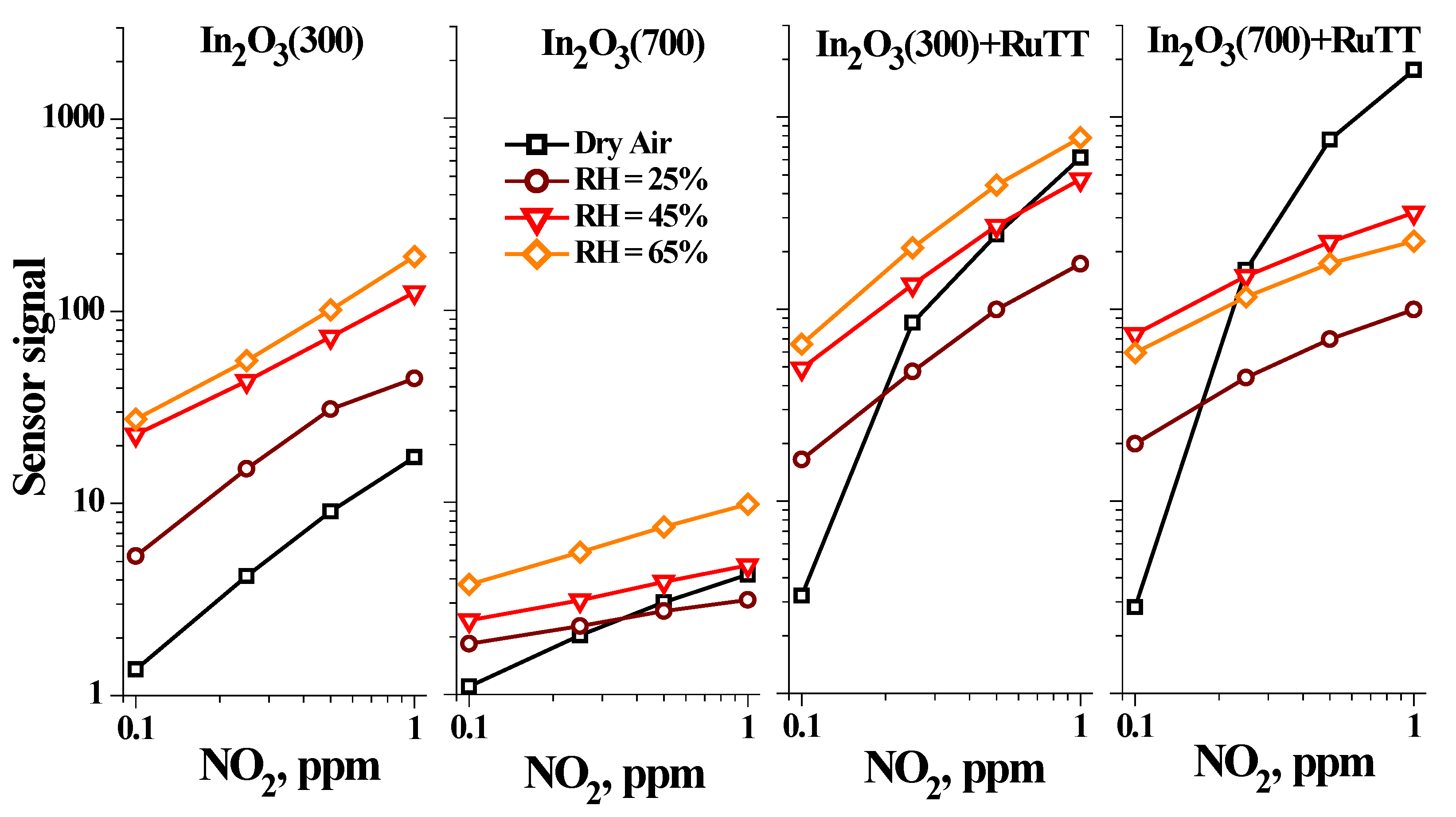
The humidity effect was studied for the samples based on In2O3 annealed at 300 and 700 °C. Figure 10 shows the dependence of the sensor signal on the NO2 concentration at different air humidity (relative humidity at 25 °C RH = 25, 45, 65%).
As can be noticed, a monotonous increase in sensor signal is observed with increasing humidity for pure oxides. It was demonstrated that in humid atmosphere the conductivity of the n-type metal oxides increases, as dissociative adsorption of H2O molecules or replacement of the chemisorbed oxygen ions can lead to release of the additional electrons into the conduction band [21,27]. The increase in the concentration of the electrons can stimulate the adsorption of the NO2 molecules [6]. Sample In2O3(300) has the largest specific surface area and, consequently, more adsorption sites; therefore, this effect is more significant for it compared to sample In2O3(700).
The hybrid materials have specific interactions with NO2 at the humid atmosphere. For the NO2 concentration below 0.25 ppm, the sensor signal increases with increasing relative humidity because of additional electrons released by the interaction with water vapor. However, for higher NO2 concentrations, the change in sensor signal in humid atmosphere is negligible comparing with the sensor signal in dry air. In this case, vacant surface active sites play vital roles as, due to their limited amount, the surface is saturated with adsorbed water and the proportion of “water electrons” becomes limited. Moreover, certain sites are already occupied by molecules of the Ru(II) heteroleptic complex in hybrid samples. Therefore, water and nitrogen dioxide molecules can compete for the same remaining adsorption sites. As the In2O3(700) sample has the smallest specific surface area, a very limited number of water molecules will be able to adsorb onto the free sites. This is additionally confirmed by the fact that with an increase in relative humidity up to 65%, the sensor signal begins to decrease and, compared to the sample In2O3(300), the sensor signal in a humid atmosphere is less.
Table 7 illustrates a comparative analysis of materials used for the detection of NO2 gas by photoactivation. Using illumination at room temperature instead of heating for activation of physical and chemical processes on the surface of the sensitive layer will significantly reduce the power consumption of sensors in the case of their practical application. An analysis of the literature data demonstrated that UV sources are mainly used for photoactivated gas sensors. The use of low-power LEDs with radiation in the visible region of the spectrum, unlike UV sources, will further reduce energy consumption and allows one to embed such sensors into compact electronic devices. The periodic illumination with a duty light cycle of 50% used in this work will further reduce the power consumption by half. The highest sensor signal is established for CdSe QD@In2O3 composite material [5] and here the authors also used a periodic illumination approach. However, the specific power was higher (20 mW/cm2 vs. 8 mW/cm2) and the response differs by one order (106 vs. 1.75 × 10⁵). Hereby, the hybrid materials based on nanocrystalline In2O3 and Ru(II) heteroleptic complex have good prospects, also like the CdSe QD@In2O3 composites, for further research and applications as low power consumption gas sensors.

4. Conclusions

Synthesized organic–inorganic hybrid materials based on the nanocrystalline In2O3 and Ru(II) heteroleptic complex demonstrated high sensitivity in NO2 (0.1–1.0 ppm) detecting at room temperature under periodic illumination with blue light (λmax = 470 nm). Surface modification of In2O3 with the heteroleptic complex leads to the growth of photosensitivity accompanied by the reproducible change in the photoresponse depending on the NO2 concentration. For pure oxides, the sensor signal correlates with the specific surface area, while for hybrid materials, both the sensor signal and photoresponse increase with increasing the matrix crystallinity; the In2O3(700)+RuTT sample demonstrated the highest values of response. In this case, the main role is played by traps of nonequilibrium charge carriers, which are structural defects in the matrix. An increase in the annealing temperature decreases their concentration, which makes it possible to accelerate the kinetics of photoconductivity.

Supplementary Materials

The following are available online at https://www.mdpi.com/article/10.3390/chemosensors10040135/s1; Scheme S1: Synthesis of Ru (II) complex.

Author Contributions

Conceptualization, M.R. and O.F.; data curation, A.N. and S.T.; formal analysis, A.N.; investigation, A.N., S.T. and I.B.; methodology, A.N., M.R. and O.F.; supervision, M.R.; writing—original draft preparation, A.N. and M.R.; writing—review and editing, A.N. and M.R. All authors have read and agreed to the published version of the manuscript.

Funding

The reported study was funded by RFBR, project number 20-33-90083.

Institutional Review Board Statement

Not applicable.

Informed Consent Statement

Not applicable.

Data Availability Statement

The data presented in this study are available upon request from the corresponding author. The data are not publicly available due to privacy reasons.

Acknowledgments

SEM experiments were carried out using research infrastructure of the “Educational and Methodical Center of Lithography and Microscopy” of the Lomonosov Moscow State University.

Conflicts of Interest

The authors declare no conflict of interest.

References

  1. Kalia, S.; Haldorai, Y. Organic-Inorganic Hybrid Nanomaterials; Springer: Berlin/Heidelberg, Germany, 2015. [Google Scholar]
  2. Kaushik, A.; Kumar, R.; Arya, S.K.; Nair, M.; Malhotra, B.D.; Bhansali, S. Organic-Inorganic Hybrid Nanocomposite-Based Gas Sensors for Environmental Monitoring. Chem. Rev. 2015, 115, 4571–4606. [Google Scholar] [CrossRef] [PubMed]
  3. Wang, S.; Kang, Y.; Wang, L.; Zhang, H.; Wang, Y.; Wang, Y. Organic/inorganic hybrid sensors: A review. Sens. Actuators B Chem. 2013, 182, 467–481. [Google Scholar] [CrossRef]
  4. Sanchez, C.; Julian, B.; Belleville, P.; Popall, M. Applications of hybrid organic–inorganic nanocomposites. J. Mater. Chem. 2005, 15, 3559–3592. [Google Scholar] [CrossRef]
  5. Chizhov, A.; Rumyantseva, M.; Vasiliev, R.; Filatova, D.; Drozdov, K.; Krylov, I.; Marchevsky, A.; Karakulina, O.; Abakumov, A.; Gaskov, A. Visible light activation of room temperature NO2 gas sensors based on ZnO, SnO2 and In2O3 sensitized with CdSe quantum dots. Thin Solid Films 2016, 618, 253–262. [Google Scholar] [CrossRef]
  6. Chizhov, A.; Vasiliev, R.; Rumyantseva, M.; Krylov, I.; Drozdov, K.; Batuk, M.; Hadermann, J.; Abakumov, A.; Gaskov, A. Light-activated sub-ppm NO2 detection by hybrid ZnO/QD nanomaterials vs. charge localization in core-shell QD. Front. Mater. 2019, 6. [Google Scholar] [CrossRef] [Green Version]
  7. Chizhov, A.S.; Rumyantseva, M.N.; Drozdov, K.A.; Krylov, I.V.; Batuk, M.; Hadermann, J.; Filatova, D.G.; Khmelevsky, N.O.; Kozlovsky, V.F.; Maltseva, L.N.; et al. Photoresistive gas sensor based on nanocrystalline ZnO sensitized with colloidal perovskite CsPbBr3 nanocrystals. Sens. Actuators B Chem. 2021, 329, 129035. [Google Scholar] [CrossRef]
  8. Rumyantseva, M.; Nasriddinov, A.; Vladimirova, S.; Fedorova, O.; Tokarev, S.; Krylov, I.; Drozdov, K.; Baranchikov, A.; Gaskov, A. Photosensitive organic-inorganic hybrid materials for room temperature gas sensor applications. Nanomaterials 2018, 8, 671. [Google Scholar] [CrossRef] [Green Version]
  9. Nasriddinov, A.; Rumyantseva, M.; Shatalova, T.; Tokarev, S.; Yaltseva, P.; Fedorova, O.; Khmelevsky, N.; Gaskov, A. Organic-inorganic hybrid materials for room temperature light-activated sub-ppm NO detection. Nanomaterials 2020, 10, 70. [Google Scholar] [CrossRef] [Green Version]
  10. Peng, L.; Qin, P.; Zeng, Q.; Song, H.; Lei, M.; Mwangi, J.J.N.; Wang, D.; Xie, T. Improvement of formaldehyde sensitivity of ZnO nanorods by modifying with Ru(dcbpy)2(NCS)2. Sens. Actuators B 2011, 160, 39–45. [Google Scholar] [CrossRef]
  11. Aghazad, S.; Nazeeruddin, M.K. Ruthenium Complexes as Sensitizers in Dye-Sensitized Solar Cells. Inorganics 2018, 6, 52. [Google Scholar] [CrossRef] [Green Version]
  12. Balasingam, S.K.; Lee, M.; Kang, M.G.; Jun, Y. Improvement of dye-sensitized solar cells toward the broader light harvesting of the solar spectrum. Chem. Commun. 2013, 49, 1471–1487. [Google Scholar] [CrossRef] [PubMed] [Green Version]
  13. Gao, F.; Wang, Y.; Shi, D.; Zhang, J.; Wang, M.; Jing, X.; Baker, R.H.; Wang, P.; Zakeeruddin, S.; Graetzel, M. Enhance the Optical Absorptivity of Nanocrystalline TiO2 Film with High Molar Extinction Coefficient Ruthenium Sensitizers for High Performance Dye-Sensitized Solar Cells. J. Am. Chem. Soc. 2008, 130, 10720–10728. [Google Scholar] [CrossRef] [PubMed]
  14. Dongare, P.; Myron, B.D.B.; Wang, L.; Thompson, D.W.; Meyer, T.J. [Ru(bpy)3]2+* revisited. Is it localized or delocalized? How does it decay? Coord. Chem. Rev. 2017, 345, 86–107. [Google Scholar] [CrossRef]
  15. Nazeeruddin, M.K.; Kay, A.; Humpbry-Baker, R.; Miiller, E.; Liska, P.; Vlachopoulos, N.; Gratzel, M. Conversion of Light to Electricity by cis-X2Bis(2,2′-bipyridyl-4,4′-dicarboxylate)ruthenium (II) Charge-Transfer Sensitizers (X = C1, Br, I, CN, and SCN-) on Nanocrystalline TiO2 Electrodes. J. Am. Chem. Soc. 1993, 115, 6382–6390. [Google Scholar] [CrossRef]
  16. Tokarev, S.; Rumyantseva, M.; Nasriddinov, A.; Gaskov, A.M.; Moiseeva, A.A.; Fedorov, Y.V.; Fedorova, O.; Jonusauskas, G. Electron injection effect in In2O3 and SnO2 nanocrystals modified by ruthenium heteroleptic complexes. Phys. Chem. Chem. Phys. 2020, 22, 8146–8156. [Google Scholar] [CrossRef] [PubMed]
  17. Rumyantseva, M.; Makeeva, E.; Gaskov, A.; Shepel, N.; Peregudova, S.; Khoroshutin, A.; Tokarev, S.; Fedorova, O. H2S Sensing by Hybrids Based on Nanocrystalline SnO2 Functionalized with Cu(II) Organometallic Complexes: The Role of the Ligand Platform. Nanomaterials 2017, 7, 384. [Google Scholar] [CrossRef] [PubMed] [Green Version]
  18. Ngoc, T.M.; Nguyen, H.; Hung, C.M.; Trung, N.N.; Duy, N.V. H2S Sensing Characteristics of Self-heated Ag-coated SnO2 nanowires. In Proceedings of the 12th Asian Conference on Chemical Sensors (ACCS2017), Hanoi, Vietnam, 12–15 November 2017. [Google Scholar]
  19. Goncharov, T.; Nasriddinov, A.; Zubenko, A.; Tokarev, S.; Khmelevsky, N.; Fedorova, O.; Rumyantseva, M. Nanocrystalline SnO2 Functionalized with Ag(I) Organometallic Complexes as Materials for Low Temperature H2S Detection. Materials 2021, 14, 7778. [Google Scholar] [CrossRef]
  20. Yamazoe, N.; Sakai, G.; Shimanoe, K. Oxide semiconductor gas sensors. Catal. Surv. Asia 2003, 7, 63–75. [Google Scholar] [CrossRef]
  21. Bârsan, N.; Weimar, U. Conduction model of metal oxide gas sensors. J. Electroceram. 2001, 7, 143–167. [Google Scholar] [CrossRef]
  22. Barsan, N.; Schierbaum, K. Gas Sensors Based on Conducting Metal Oxides. Basic Understanding, Technology and Applications; Metal Oxides Series; Elsevier: Amsterdam, The Netherlands, 2019. [Google Scholar]
  23. Orlandi, M.O. Tin Oxide Materials: Synthesis, Properties, and Applications; Metal Oxides Series; Elsevier: Amsterdam, The Netherlands, 2020. [Google Scholar]
  24. Lin, T.; Lv, X.; Li, S.; Wang, Q. The Morphologies of the Semiconductor Oxides and Their Gas-Sensing Properties. Sensors 2017, 17, 2779. [Google Scholar] [CrossRef] [Green Version]
  25. Forsh, E.A.; Marikutsa, A.V.; Martyshov, M.N.; Forsh, P.A.; Rumyantseva, M.N.; Gaskov, A.M.; Kashkarov, P.K. A Study of the Sensitivity of Nanocrystalline Indium Oxide with Various Sizes of Nanocrystals to Nitrogen Dioxide. Nanotechnologies Russ. 2012, 7, 164–168. [Google Scholar] [CrossRef]
  26. Forsh, E.A.; Marikutsa, A.V.; Martyshov, M.N.; Forsh, P.A.; Rumyantseva, M.N.; Gaskov, A.M.; Kashkarov, P.K. Charge Carrier Transport in Indium Oxide Nanocrystals. J. Exp. Theor. Phys. 2010, 111, 653–658. [Google Scholar] [CrossRef]
  27. Nasriddinov, A.; Rumyantseva, M.; Konstantinova, E.; Marikutsa, A.; Tokarev, S.; Yaltseva, P.; Fedorova, O.; Gaskov, A. Effect of Humidity on Light-Activated NO and NO2 Gas Sensing by Hybrid Materials. Nanomaterials 2020, 10, 915. [Google Scholar] [CrossRef] [PubMed]
  28. White, W.B.; Keramidas, V.G. Vibrational spectra of oxides with the C-type rare earth oxide structure. Spectrochim. Acta 1972, 28, 501–509. [Google Scholar] [CrossRef]
  29. Kranert, C.; Schmidt-Grund, R.; Grundmann, M. Raman active phonon modes of cubic In2O3. Phys. Status Solidi RRL 2014, 8, 554–559. [Google Scholar] [CrossRef]
  30. Garcia-Domene, B.; Ortiz, H.M.; Gomis, O.; Sans, J.A.; Manjon, F.J.; Munoz, A.; Rodrıguez-Hernandez, P.; Achary, S.N.; Errandonea, D.; Martınez-Garcıa, D.; et al. High-pressure lattice dynamical study of bulk and nanocrystalline In2O3. J. Appl. Phys. 2012, 112, 123511. [Google Scholar] [CrossRef]
  31. Kim, W.J.; Pradhan, D.; Sohn, Y. Fundamental nature and CO oxidation activities of indium oxide nanostructures: 1D-wires, 2D-plates, and 3D-cubes and donuts. J. Mater. Chem. A 2013, 1, 10193. [Google Scholar] [CrossRef]
  32. Mott, N.F.; Devis, E.A. Electron Processes in Non-Crystalline Materials; Clarendon press: Oxford, UK, 1979. [Google Scholar]
  33. Wagner, T.; Kohl, C.D.; Malagù, C.; Donato, N.; Latino, M.; Neri, G.; Tiemann, M. UV Light-Enhanced NO2 Sensing by Mesoporous In2O3: Interpretation of Results by a New Sensing Model. Sens. Actuators B Chem. 2013, 187, 488–494. [Google Scholar] [CrossRef]
  34. Ilin, A.; Martyshov, M.; Forsh, E.; Forsh, P.; Rumyantseva, M.; Abakumov, A.; Gaskov, A.; Kashkarov, P. UV Effect on NO2 Sensing Properties of Nanocrystalline In2O3. Sens. Actuators B Chem. 2016, 231, 491–496. [Google Scholar] [CrossRef]
  35. Zhang, C.; Boudiba, A.; De Marco, P.; Snyders, R.; Olivier, M.G.; Debliquy, M. Room Temperature Responses of Visible-Light Illuminated WO3 Sensors to NO2 in Sub-Ppm Range. Sens. Actuators B Chem. 2013, 181, 395–401. [Google Scholar] [CrossRef]
  36. Mun, Y.; Park, S.; An, S.; Lee, C.; Kim, H.W. NO2 Gas Sensing Properties of Au-Functionalized Porous ZnO Nanosheets Enhanced by UV Irradiation. Ceram. Int. 2013, 39, 8615–8622. [Google Scholar] [CrossRef]
  37. Karaduman, I.; Yildiz, D.E.; Sincar, M.M.; Acar, S. UV Light Activated Gas Sensor for NO2 Detection. Mater. Sci. Semicond. Process. 2014, 28, 43–47. [Google Scholar] [CrossRef]
  38. Park, S.; Kim, S.; Ko, H.; Lee, C. Light-Enhanced Gas Sensing of ZnS-Core/ZnO-Shell Nanowires at Room Temperature. J. Electroceramics 2014, 33, 75–81. [Google Scholar] [CrossRef]
  39. Park, S.; Ko, H.; Lee, S.; Kim, H.; Lee, C. Light-Activated Gas Sensing of Bi2O3-Core/ZnO-Shell Nanobelt Gas Sensors. Thin Solid Films 2014, 570, 298–302. [Google Scholar] [CrossRef]
  40. Zhang, C.; Wang, J.; Olivier, M.G.; Debliquy, M. Room Temperature Nitrogen Dioxide Sensors Based on N719-Dye Sensitized Amorphous Zinc Oxide Sensors Performed under Visible-Light Illumination. Sens. Actuators B Chem. 2015, 209, 69–77. [Google Scholar] [CrossRef]
  41. Park, S.; Sun, G.J.; Kheel, H.; Ko, T.; Kim, H.W.; Lee, C. Light-Activated NO2 Gas Sensing of the Networked CuO-Decorated ZnS Nanowire Gas Sensor. Appl. Phys. A Mater. Sci. Process. 2016, 122, 504. [Google Scholar] [CrossRef]
  42. Chizhov, A.S.; Rumyantseva, M.N.; Vasiliev, R.B.; Filatova, D.G.; Drozdov, K.A.; Krylov, I.V.; Abakumov, A.M.; Gaskov, A.M. Visible Light Activated Room Temperature Gas Sensors Based on Nanocrystalline ZnO Sensitized with CdSe Quantum Dots. Sens. Actuators B Chem. 2014, 205, 305–312. [Google Scholar] [CrossRef]
  43. Espid, E.; Taghipour, F. Development of Highly Sensitive ZnO/In2O3 Composite Gas Sensor Activated by UV-LED. Sens. Actuators B Chem. 2017, 241, 828–839. [Google Scholar] [CrossRef]
  44. Zhou, Y.; Zou, C.; Lin, X.; Guo, Y. UV Light Activated NO2 Gas Sensing Based on Au Nanoparticles Decorated Few-Layer MoS2 Thin Film at Room Temperature. Appl. Phys. Lett. 2018, 113, 2–7. [Google Scholar] [CrossRef]
  45. Casals, O.; Markiewicz, N.; Fabrega, C.; Gràcia, I.; Cane, C.; Wasisto, H.S.; Waag, A.; Prades, J.D. A Parts per Billion (Ppb) Sensor for NO2 with Microwatt (ΜW) Power Requirements Based on Micro Light Plates. ACS Sens. 2019, 4, 822–826. [Google Scholar] [CrossRef] [Green Version]
  46. Paolucci, V.; Emamjomeh, S.M.; Ottaviano, L.; Cantalini, C. Near Room Temperature Light-Activated WS2-Decorated RGo as NO2 Gas Sensor. Sensors 2019, 19, 2617. [Google Scholar] [CrossRef] [PubMed] [Green Version]
  47. Espid, E.; Noce, A.S.; Taghipour, F. The Effect of Radiation Parameters on the Performance of Photo-Activated Gas Sensors. J. Photochem. Photobiol. A Chem. 2019, 374, 95–105. [Google Scholar] [CrossRef]
  48. Tian, X.; Yang, X.; Yang, F.; Qi, T. A Visible-Light Activated Gas Sensor Based on Perylenediimide-Sensitized SnO2 for NO2 Detection at Room Temperature. Colloids Surf. A Physicochem. Eng. Asp. 2019, 578, 123621. [Google Scholar] [CrossRef]
  49. Feng, C.; Wen, F.; Ying, Z.; Li, L.; Zheng, X.; Zheng, P.; Wang, G. Polypeptide-Assisted Hydrothermal Synthesis of ZnO for Room Temperature NO2 Gas Sensor under UV Illumination. Chem. Phys. Lett. 2020, 754, 137745. [Google Scholar] [CrossRef]
  50. Chen, C.; Zhang, Q.; Xie, G.; Yao, M.; Pan, H.; Du, H.; Tai, H.; Du, X.; Su, Y. Enhancing Visible Light-Activated NO2 Sensing Properties of Au NPs Decorated ZnO Nanorods by Localized Surface Plasmon Resonance and Oxygen Vacancies. Mater. Res. Express 2020, 7, 015924. [Google Scholar] [CrossRef]
  51. Zhang, Q.; Xie, G.; Xu, M.; Su, Y.; Tai, H.; Du, H.; Jiang, Y. Visible Light-Assisted Room Temperature Gas Sensing with ZnO-Ag Heterostructure Nanoparticles. Sens. Actuators B Chem. 2018, 259, 269–281. [Google Scholar] [CrossRef]
  52. Kumar, R.R.; Murugesan, T.; Dash, A.; Hsu, C.H.; Gupta, S.; Manikandan, A.; Anbalagan, k.A.; Lee, C.H.; Tai, N.H.; Chueh, Y.L.; et al. Ultrasensitive and Light-Activated NO2 Gas Sensor Based on Networked MoS2/ZnO Nanohybrid with Adsorption/Desorption Kinetics Study. Appl. Surf. Sci. 2021, 536, 147933. [Google Scholar] [CrossRef]
  53. Liu, Y.; Zhang, J.; Li, G.; Liu, J.; Liang, Q.; Wang, H.; Zhu, Y.; Gao, J.; Lu, H. In2O3–ZnO Nanotubes for the Sensitive and Selective Detection of Ppb-Level NO2 under UV Irradiation at Room Temperature. Sens. Actuators B Chem. 2022, 355, 131322. [Google Scholar] [CrossRef]
Figure 1. Microelectronic hotplate (a) before and (b) after deposition of a thick semiconductor film on the substrate and (c) after sensitization with a Ru(II) heteroleptic complex; SEM images of the sensitive layer deposited on the substrate, (d) side view and (e) top view.
Chemosensors 10 00135 g001
Figure 2. X-ray diffraction patterns (a) and Raman spectra (b) of nanocrystalline In2O3 samples.
Chemosensors 10 00135 g002
Figure 3. TPR-H2 curves (a) and FTIR spectra (b) of nanocrystalline In2O3 samples with different annealing temperatures.
Chemosensors 10 00135 g003
Figure 4. Temperature dependence of conductivity of the In2O3(300), In2O3(500) and In2O3(700) samples in Mott coordinates in the temperature range of 140–25 °C.
Chemosensors 10 00135 g004
Figure 5. Optical absorption spectra (a,b) and normalized spectral dependences of the photoconductivity (c,d) of pure semiconductors and hybrid materials.
Chemosensors 10 00135 g005
Figure 6. Change in the conductivity of pure In2O3 with different grain sizes (a) and hybrid materials (b) under dark and irradiation conditions.
Chemosensors 10 00135 g006
Figure 7. Photoresponse of synthesized samples.
Chemosensors 10 00135 g007
Figure 8. Change in resistance of the pure oxides and hybrid materials under periodic illumination with blue LED in the presence of various NO2 concentrations for (a) In2O3(300) based, (b) In2O3(500) based, (c) In2O3(700) based samples.
Chemosensors 10 00135 g008
Figure 9. Dependence of the sensor signal (a) and photoresponse (b) of In2O3(300), In2O3(500), In2O3(700) samples and hybrid materials based on them on the concentration of NO2.
Chemosensors 10 00135 g009
Figure 10. Dependence of the sensor signal of In2O3(300), In2O3(700) samples and hybrid materials based on them on the NO2 concentration at different air humidity (relative humidity at 25 °C RH = 25, 45, 65%).
Chemosensors 10 00135 g010
Table 1. Structural formula, the energies of HOMO and LUMO and the label of the Ru(II) heteroleptic complex.
StructureEHOMO, eVELUMO, eVLabelName
Chemosensors 10 00135 i0012Cl−6.15−3.46RuTTbis(2,2′-bipyridin-k2N1,N1′)[2-(2,2′-bithiophen-5-yl)-1H-imidazo[4,5-f][1,10]phenanthroline-k2N7,N8) ruthenium (II) dichloride
Table 2. Phase composition, crystallite size (dXRD) and specific surface area (Ssurf) of nanocrystalline In2O3 samples annealed at temperatures of 300, 500 and 700 °C.
SamplePhase CompositiondXRD, nmSsurf, m2/g
In2O3(300) 13 ± 172 ± 3
In2O3(500)In2O3 bixbyite24 ± 26 ± 1
In2O3(700) 28 ± 23 ± 1
Table 3. The results of the TPR-H2 experiments.
SampleH2 Consumption, mol H2 per 1 mol In2O3
Total25–400 °C400–900 °CTmax, °C
In2O3(300)3.0 ± 0.10.12 ± 0.012.88 ± 0.1582
In2O3(500)3.2 ± 0.10.05 ± 0.013.15 ± 0.1589
In2O3(700)3.3 ± 0.10.06 ± 0.013.24 ± 0.1589
Table 4. Parameters characterizing the conductivity of the studied samples according to the Mott model for In2O3(300), In2O3(500) and In2O3(700) samples.
SampleTM × 109, KN(EF) × 1017, eV−1 ×cm−3Rhop, nmWhop, eV
25 °C140 °C25 °C140 °C
In2O3(300)14.50.2426.0524.010.550.7
In2O3(500)3.51.0118.2616.830.380.49
In2O3(700)1.163.0513.8512.770.290.37
Table 5. Elemental composition of hybrid materials.
Sample[Ru]/([Ru] + [In]), wt.%[In]/([Ru] + [In]), wt.%
In2O3(300)+RuTT0.53 ± 0.0199.47 ± 0.13
In2O3(500)+RuTT0.58 ± 0.0199.42 ± 0.11
In2O3(700)+RuTT0.54 ± 0.0199.46 ± 0.12
Table 6. Baseline resistance in dark conditions and under LED illumination in dry air at room temperature.
SampleR (Dark), OhmR (Light), Ohm
In2O3 (300)7.6 × 103103
In2O3 (500)2.6 × 1034.6 × 102
In2O3 (700)7.2 × 1024.0 × 102
In2O3 (300) + RuTT1.6 × 1066.5 × 105
In2O3 (500) + RuTT5.3 × 1059.4 × 104
In2O3 (700) + RuTT4.2 × 1058.6 × 104
Table 7. Comparison of the light-activated (with LED) NO2 gas sensor performances at room temperature for different materials.
MaterialWavelength, nmIncident Irradiance, mW/cm2NO2 Concentration, ppmSensor Signal (a), % Ref.
Mesoporous In2O3400-5.0900[33]
In2O33851.08.017,900[34]
WO35903400.16820[35]
Au/ZnO3651.25.0455[36]
Al/TiO2/Al2O3/p-Si254-2011.5[37]
ZnS-core/ZnO-shell nanowires2541.21.0339[38]
Bi2O3-core/ZnO-shell nanobelt2541.21.0227[39]
N-719 dye/ZnO hybrid4803701.25143[40]
CuO/ZnS nanowire3652.25.0955[41]
CdSe QD@In2O3535201.6106[5]
CdSe QD@ZnO535201.63000[5,42]
ZnO/In2O3 composite365255221[43]
Au/MoS2365-2.530[44]
ZnO45550.02520[45]
WS2-decorated rGO4300.661.021[46]
ZnO/(ZnSe(shell) @CdS(core)) composite535202.06900[6]
WO336585.011,300[47]
Perylenediimide-sensitized SnO2400–700-0.512,900[48]
Polypeptide-assisted ZnO nanorods365-10.0400[49]
Au-ZnO nanorods495501.0109[50]
Ag- ZnO heterostructure470751.0150[51]
MoS2/ZnO nanohybrid3650.30.52310[52]
ZnO/CsPbBr3 NCs4708.02.030,000[7]
In2O3–ZnO nanotubes3651.950.53170[53]
In2O3/Ru(II) heteroleptic complex4708.01.01.75 × 105This work
(a) The sensor signals were recalculated as S = R ( NO 2 ) R ( air ) R ( air )   × 100%.
Publisher’s Note: MDPI stays neutral with regard to jurisdictional claims in published maps and institutional affiliations.

