1. Introduction
The proportional–integral (PI) regulation scheme is a widely used control technique for several real-time systems such as process controls, power converters, motor speed control, etc. [
1,
2,
3,
4]. In this scheme, the proportional and integral actions act on an error value, which is derived by subtracting the actual output from its reference. The output of a PI controller is a control signal that changes the manipulated variable to regulate the output. The key benefits of this control scheme are it improves the transient response, removes the steady-state error, and is easy to implement. Specifically, the proportional action in the controller is mainly used to increase the speed of the response (and thus reduce the settling time), and an integral action is mainly responsible for accurately tracking the output to the required reference value. As an example, in the case of power electronic DC–DC systems, often the output voltage varies with respect to changes in the load and input voltage. However, since this output voltage acts as a source for subsequent power stages, it needs to be maintained constant irrespective of such variations in the parameters. To achieve this goal, a PI controller can be employed. In this method, the actual voltage is sensed, then compared with a reference, and the error signal is obtained. The PI controller then acts on this error signal, and a control signal in the form of the required duty ratio is generated [
5,
6]. When the output voltage decreases below the reference value, the error signal increases, which increases the control signal and duty ratio to allow for a further increase in the output voltage to reach the reference value again. Similarly, when the output voltage becomes higher than the reference value, the error signal and subsequent control signal decrease accordingly to decrease the output voltage again to reach the reference.
Even though such a PI controller has a wide range of applications, it has certain limitations. These limitations are mainly evident when considerably higher values of controller gains are employed to achieve a faster transient response. When higher values of gain (especially a large integral gain) are employed to improve the transient and steady-state responses, there is a possibility that the control signal could take very high values in the occurrence of large system errors and may saturate too. This is because the integrand (the term on which the integrator action acts) in a traditional PI controller is the system’s error signal itself. This problem can be alleviated by employing a saturation block at the output of the PI controller. This block can limit the maximum value of the control signal. However, during the saturation, the feedback loop is broken and the system operates in an open-loop mode. This may lead to a loss of control actions and could also lead to instability. Secondly, control system analysis based on the saturation block is not an easy task. Considering all these factors, there is a scope to improve the structure of the orthodox PI scheme to address these concerns.
In the present article, an improved normalized error-based PI controller is proposed. The main benefit of the controller lies in the fact that it acts on a normalized error signal, which is always bounded even if the actual system’s error is large. Thus, there is no risk of unbounded control signals or saturation even if larger values of controller gains are employed. This provides more room for choosing the controller’s constants to achieve a smoother response. In this scheme, the structure of the normalized error term is chosen such that its maximum value is limited by an operator-specified number. The detailed structure of the orthodox PI control scheme is presented and its drawbacks are explained. Later, the generic form of the proposed normalized error-based PI scheme is illustrated and its advantages are described in both theoretical and graphical ways.
Second, the output voltage control of the step-down DC–DC system is used to validate the efficacy of the normalized PI controller. DC–DC power electronic converters are used in diverse industrial settings, including telecommunications, electric cars, and systems based on non-conventional energy resources [
7,
8,
9,
10,
11]. For instance, the auxiliary components of an electric car require an input voltage that is substantially lower than the battery voltage. Therefore, in this application, a step-down power converter with a proper conversion ratio is appropriate. In many of these applications, wherein there are parameter fluctuations like load-side and input supply variances, tight voltage control is necessary. In summary, an appropriate controller needs to be employed along with a step-down converter to achieve load-side voltage regulation.
Among the two main types of power converters dealing with DC voltages (viz. buck and boost converters), the control of the load voltage of the buck converter can be achieved using a direct method, i.e., by sensing the voltage directly. But for the step-up converters, where the voltage control must be accomplished indirectly, primarily due to the occurrence of zeroes in the open-loop transfer function on the right side of the s-plane, this is not the case [
12,
13]. Even though the control implementation of step-down buck converters is straightforward, there are certain difficulties that need to be resolved. The main concern is that there is a tradeoff between the ability of the controller to effectively handle small parameter variations and its capability to ensure stability in the presence of large parameter variations. For instance, in direct voltage control for the buck converters, the output of the control block is the control signal, which is used to synthesize the switching signal. In this case, if large controller gains are used, the control signal could saturate and the system could become unstable. If small values of gains are employed to overcome this issue, the system’s response could become slower. To address this concern, in this article, the proposed normalized error-based PI regulation scheme is used to achieve the regulation of the power buck converter. Stability analysis using two separate controllers viz. a traditional PI controller and an improved normalized error-based PI controller is illustrated and the advantages of the proposed scheme in that it provides a higher range of gain for stability are highlighted. Additionally, some tuning recommendations that show how the control scheme’s gains affect the quality of the output response are given. Finally, some simulation outcomes are shown, which confirm the capability of the normalized PI scheme to overcome changes in the load, input, and desired voltage levels.
The article is structured as follows: In
Section 2, the motivation and background of the normalized PI controller is given. In
Section 3, the design and comparative study of the traditional PI scheme and the normalized PI scheme for the buck system are given. Some simulation outcomes are then provided in
Section 4 to support the theoretical outcomes. The last section is a conclusion.
2. Structure of the Proposed Normalized Error-Based PI Controller
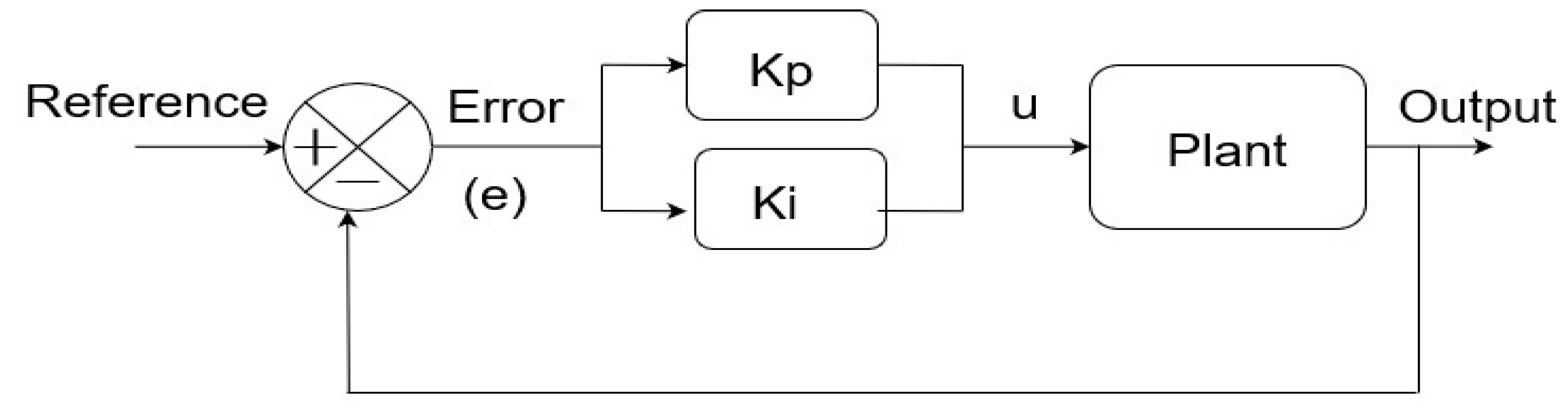
Initially, the motivation behind the normalized error-based PI controller is presented. To this end, the drawbacks of the traditional PI scheme are discussed first. The structure of the traditional PI scheme is shown in
Figure 1, and this is to be depicted as
Here, represents the control signal, and are the control scheme’s constants of the system, and depicts an error signal.
Figure 1.
Block schematic of the orthodox PI scheme.
Figure 1.
Block schematic of the orthodox PI scheme.
In (1), the integrand (the term on which the integrator operates) is the system error itself. When sufficiently high values of control scheme constants are used and when an error is also significant, such as during the transient part of the response, the integrand can take very large values and the controller output may saturate. If lower values of controller gains are employed, it could affect the speed of the response in the presence of the converter’s parameter fluctuations. Thus, there is a trade-off between the controller response for larger error values and the transient response for system parameter variations. Secondly, if a saturation block is introduced, the system acts like an open loop.
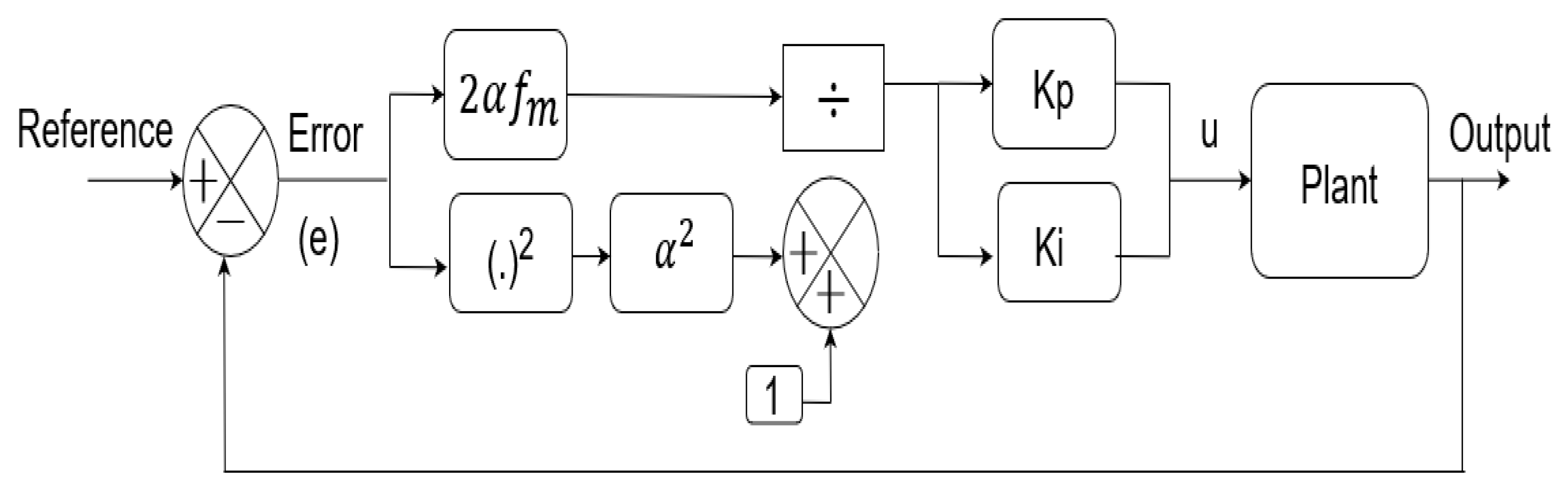
Thus, to overcome these limitations of the traditional PI controller, a normalized PI controller is proposed. Adaptive laws with normalization are used in adaptive control as discussed in [
14]. The form of this improved PI scheme, as shown in
Figure 2, is given by
where
and
are the proportional and integral gains of the controllers and
and
are additional gains available for tuning, which decide the maximum value of the control signal as discussed below. Also,
and
depict the control signal and an error signal, respectively.
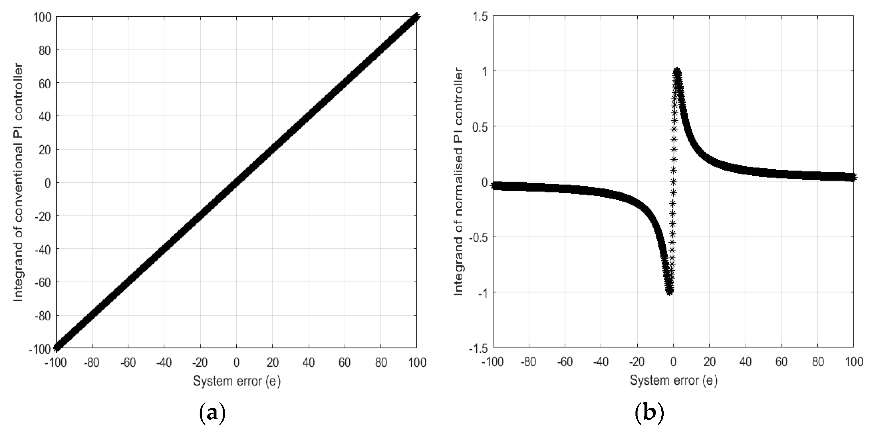
In order to calculate the maximum range of
, we need to find
and equate it with zero.
Equating
, we obtain
. Substituting this in
, we obtain
where
is the maximum value of function
.
This proves that the highest value of the normalized error is confined by a user-defined fixed value, i.e., .
Figure 3 compares the integrand of the traditional PI controller vs. the integrand of the normalized error-based PI controller (using
) graphically. It can be seen that the integrand of the traditional PI controller increases without any bound as the value of the error signal increases. However, the integrand of the normalized error-based PI controller is limited by
.
3. Normalized Error-Based PI Scheme for the DC–DC Step-Down Converter
Next, the use of the normalized error-based PI regulation controller for the step-down power converter is illustrated. Initially, the controller design using the orthodox PI controller is shown and the range of the controller gain is determined to guarantee the stable region. Next, the control scheme based on the bounded error signal is applied to the same converter topology to show improvements in the range for the control scheme’s constants to achieve stability.
- A.
Modeling of step-down power converter using averaged state-space method
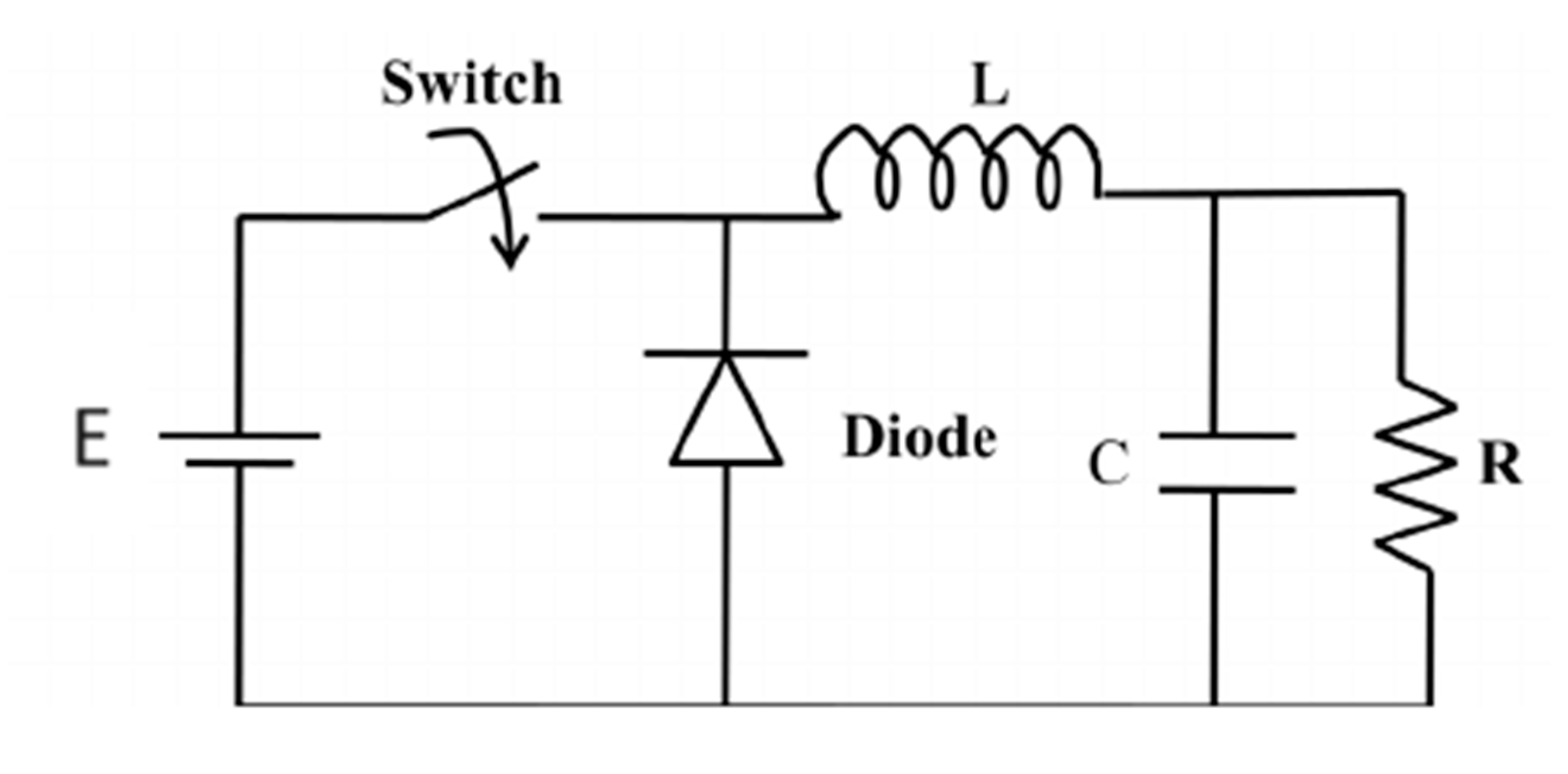
First, the model of the step-down power converter is created using the averaged state-space method. This model is shown because it aids the control scheme design later.
Figure 4 depicts the circuit schematic of the power step-down converter.
The model of the system in the state-space form is given by
where
and
are the system state variables, which depict the current in an inductor and loa-side voltage, respectively, and
and
depict the nominal values of the source and load, respectively. Also,
depicts the duty ratio such that
.
By setting (7) and (8) to zero, the resulting equilibrium values are shown as
where
is the system’s nominal voltage level and
and
are the nominal values of
and
respectively.
- B.
PI Controller analysis for the step-down power converter
Now, the detailed design and stability of the PI regulation scheme for the step-down converter is shown.
Initially, the following error terms are defined:
The control objective is to make
. To achieve this, the PI control law for regulating the output voltage is given by
where
and
depict the user-defined proportional and integral constants for the converter. Also,
is the control signal and
is the nominal value of the duty ratio such that
.
In order to investigate the system stability, the error dynamics are derived.
Using (7)–(11) yields the following error dynamics:
The necessary equilibrium points for (12)–(14) are depicted by.
Next, a Lypunov indirect method-based [
15] stability study is conducted. Linearization of (12)–(14) around the equilibrium point given by
yields the following linearized system of the form [
16]:
where
,
,
,
and the matrix
is
Now, for the matrix
, its eigenvalues must stay in the LHS of the s-plane so that the system remains stable. It also means that the characteristic equation (
) should have roots that lie in the left-hand side of the s-plane. It is possible to select the controller gain’s range for
, and
to guarantee that all the eigenvalues of
have negative real parts. The following values of the buck converter are selected for an illustration purpose:
The root locus method may be employed to inspect the stable region of the closed-loop converter considering the high order of the polynomial
. In the mentioned approach, one control scheme’s parameter, say
, is fixed and the rest of the scheme’s parameters, such as
, are manipulated till the eigenvalues of
M leave the stable region in the s-plane. To this end, for demonstration purposes, we have used
and varied
such that
[
2].
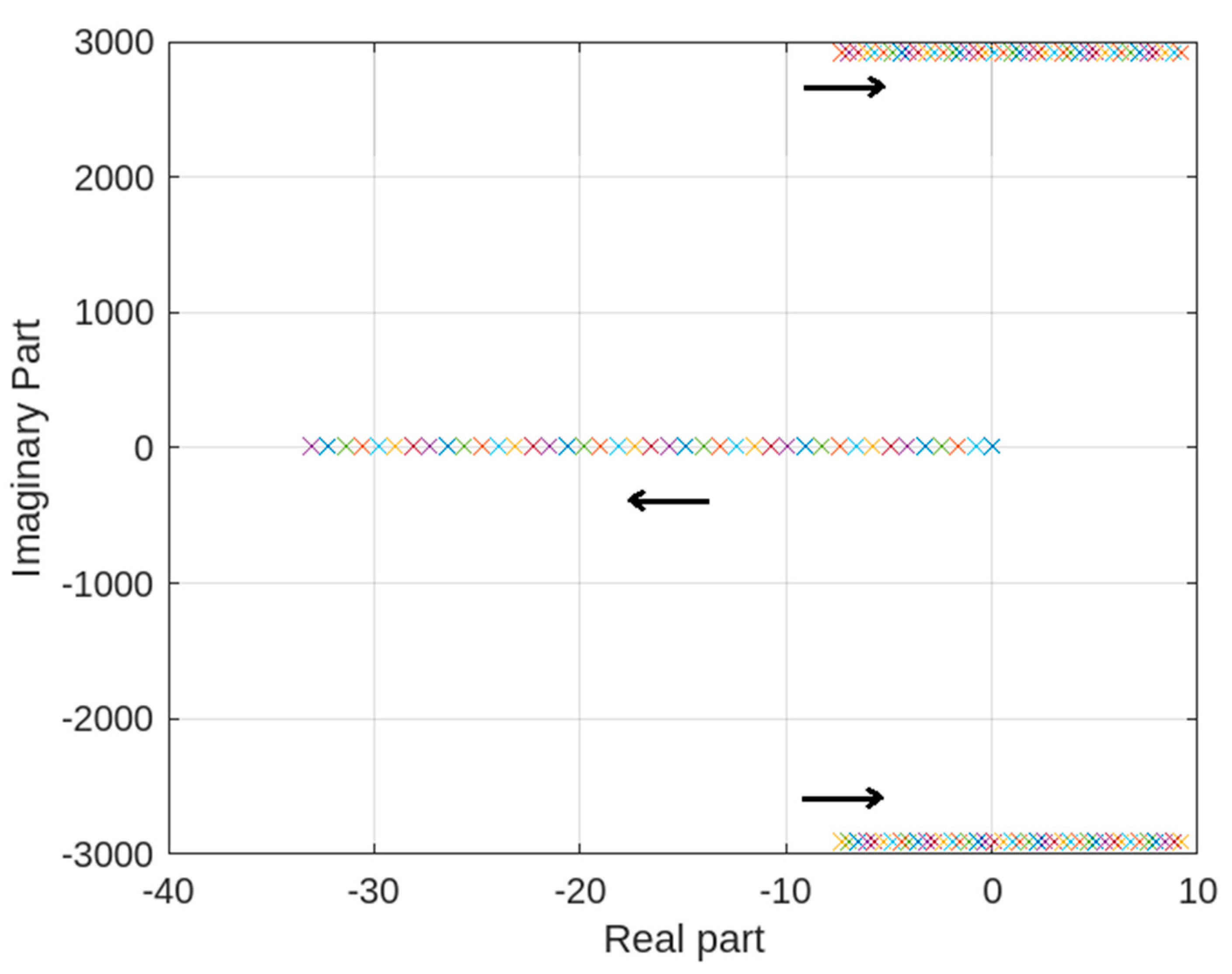
Figure 5 depicts the root locus graph of
. The arrow shows how poles or eigenvalues are moving when
increases from 0 to 4. It was found that the system is stable when
. When
, the roots left the stable region of the s-plane.
- C.
Normalized error-based PI Controller analysis for the step-down buck power system
Next, the controller design using the proposed normalized error-based PI controller is carried out. The new error terms are defined:
To achieve the control objective of
, the normalized error-based PI controller is given by
where
is the proposed control law and
is its steady-state value given by
. Also,
,
,
and
are the user-defined proportional and integral gains of the converter. Again, in order to investigate the system stability, the error dynamics are derived and using (7)–(9), (18), and (19) yields the following error dynamics given by (20)–(22):
The necessary steady-state equilibrium points of (20)–(22) can be written as.
Using the Lypunov indirect method again, the linearization of (20)–(22) around the equilibrium point given by
, leads to the system in the linearized form depicted by
where
,
,
,
. The matrix
is obtained by assuming
and thus
. It is given by
Using similar values of circuit parameters as used in (17), the roots of the system characteristic equation
are plotted. Again, the controller parameters
,
, and
are fixed to
,
, and
and the roots are plotted for varying
.
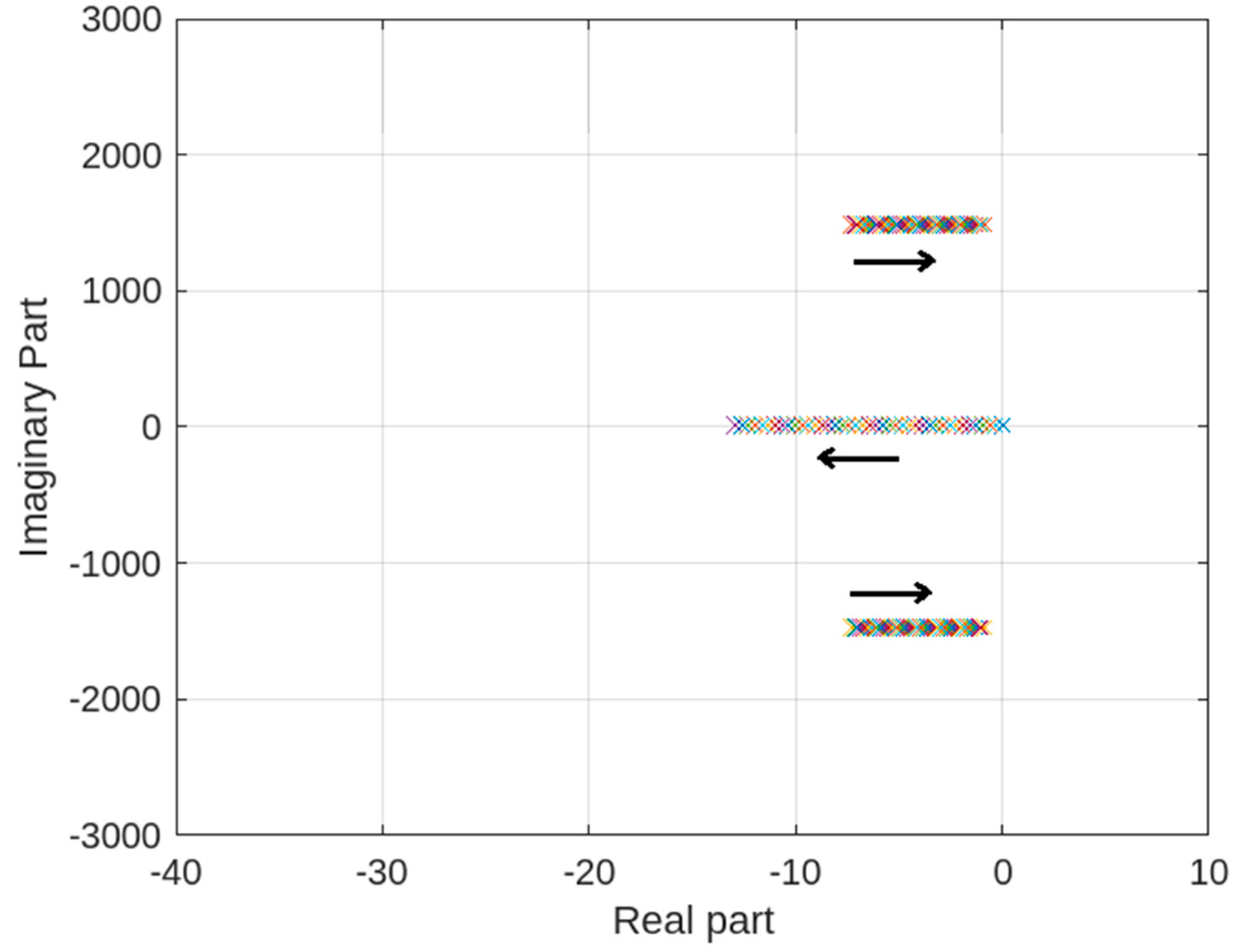
Figure 6 depicts the root locus graph for
. The arrow shows how poles or eigenvalues are moving when
increases from 0 to 4. It was seen that the converter system remains in the stable area for the full range of
.
It can be observed that unlike the case of the orthodox PI control scheme, the proposed control scheme has a wider choice of controller parameters available for tuning (refer to
Section 4A) and it also provides two additional parameters,
, and
for tuning purposes.
Further Discussions: In this section, the issue of regulation of the load-side voltage of the step-down power converter using the traditional PI control scheme and an improved normalized error-based PI controller is addressed. However, it is important to highlight that the form of the presented control scheme given by (19) is not confined to any specific converter and can be suitably used for regulating the load-side voltage of other advanced topologies such as high-order buck converters [
17,
18] and non-minimum phase boost-type converters [
19,
20]. The control of non-minimum phase boost converters is especially challenging because their open-loop transfer function (with the output voltage in the numerator and the control signal in the denominator) have zeroes on the right side of the s-plane. Thus, it is not an easy task to achieve load voltage control employing a single voltage loop like what is shown in
Figure 6. However, their control can be achieved by employing a dual loop in which the inner loop is the inductor current and its reference is generated using an outer voltage loop [
21]. The proposed normalized error-based PI controller still finds its application in such converters because state-of-the-art dual-loop controllers often employ either two individual PI controllers in the inner and outer loops separately or at least one PI controller in one of the two loops [
5,
22]. In such applications, the PI controller can be replaced by an improved PI controller and this topic requires further investigation to authenticate the use of the proposed control scheme for such dual-loop systems.
Secondly, even though the main objective of this paper is to introduce the idea of the normalized error-based PI controller, it is worth mentioning that the proposed controller can be combined with other advanced controllers such as the hysteresis modulation-based sliding-mode (SM) control and the dual-loop current-mode control. For instance, in [
6], the hysteresis-based SM control of the quadratic boost converter is given. In this scheme, a dual-loop scheme is employed in which the inner current loop is based on an SM control and an outer voltage loop is based on a PI control that acts upon a plain voltage error. Similarly, in [
5], a dual-loop current-mode controller for the Luo converter is designed. In both such schemes, the outer voltage loop can be modified to be based on the normalized error signal and a bounded reference signal can be generated for the inner-loop current controller. This is the future scope of our paper.
4. Simulation Outcomes
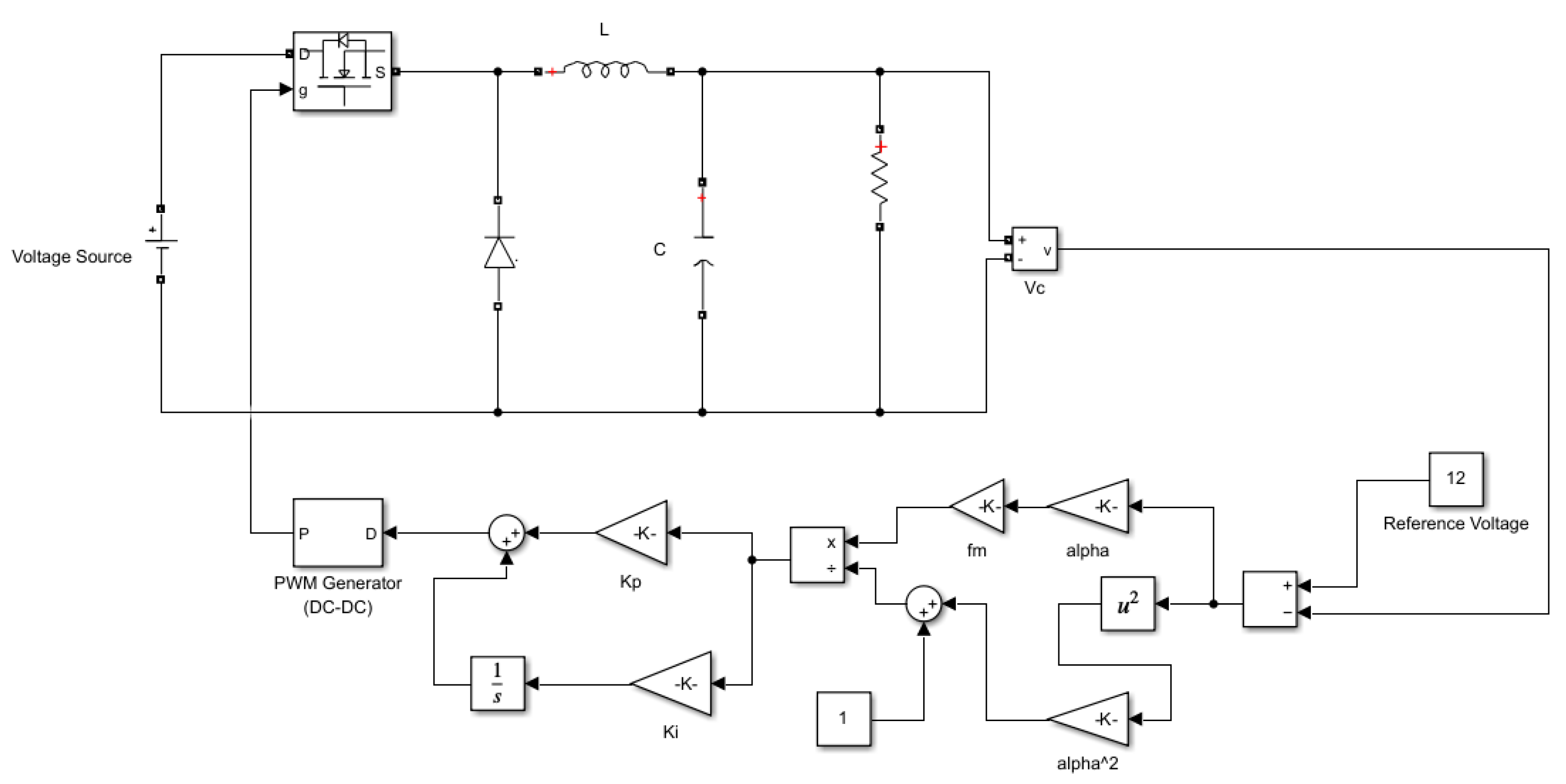
Some simulations and their results are presented in this part to support the conclusions drawn from the theory. The presented normalized error-based PI controller is implemented in MATLAB Simulink 2022b. The Simulink diagram is illustrated in
Figure 7. The same set of converter parameters as used in (17) was used for simulations.
- A.
Tuning of proposed controller gains
There are four controller gains (i.e.,
,
, and
) available for tuning. Considering a higher order of the system given by (23) (and this order can be further increased if the proposed controller is applied to some advanced high-order topologies like those used in [
2,
5]), a generic heuristic approach of the controller gain tuning is employed. To this end, initially, the range of controller gains that ensure stability can be determined using the root locus technique as described in
Section 3C. Next, in order to fine-tune the gain parameters, one controller gain is varied at a time by keeping the values of the other three gains fixed. The optimum value of the gain is then obtained to achieve the least overshoot and settling time. The detailed procedure is explained below.
Initially, the result of varying
on the output curve was studied and other parameters
,
, and
were set to 1, 0.1, and 1, respectively. The resistance was changed from its nominal value of
to
at t = 1 s and again bought back to
at time t = 1.5 s and the response for varying
from 0.1 to 0.5 was plotted.
Figure 8 shows the corresponding output curve for various
values. It can be observed that as
increases, the overshoot of the transient curve increases. Thus, a lower value of
is preferred to obtain a better transient curve. The load-change response can then be adjusted with other gain values.
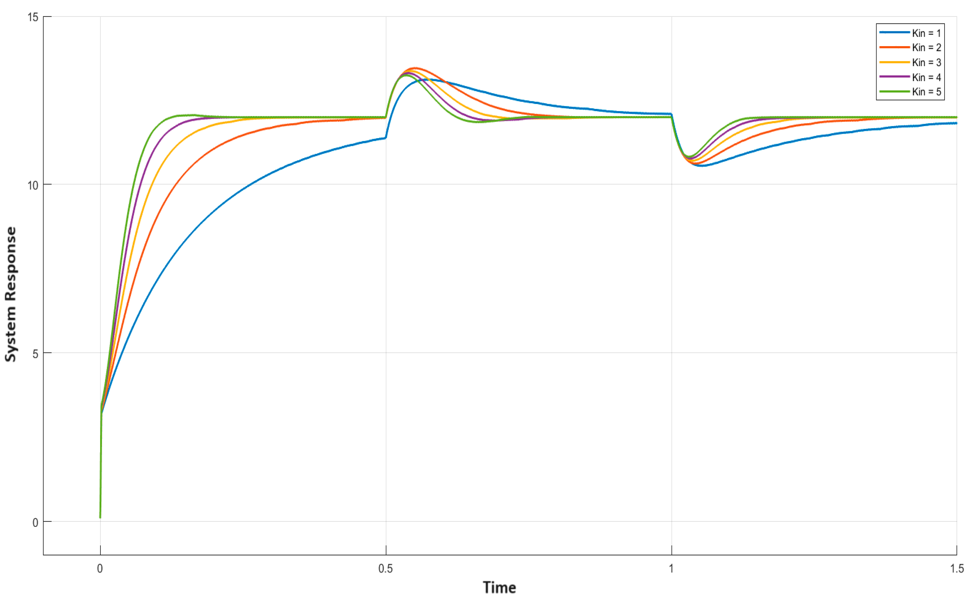
Next, the consequence of varying
on the overall output curve was examined and other parameters
,
, and
were set to 0.1, 0.1, and 1, respectively. Again, for a similar change in the load, the response for varying
from 1 to 5 was plotted.
Figure 9 shows the corresponding output curves of the system. It is easily observable that as
increases, the settling time of the load-change curve reduces noticeably while overshoot almost remains the same. Thus, a higher value of
is preferred to obtain a better load-change curve.
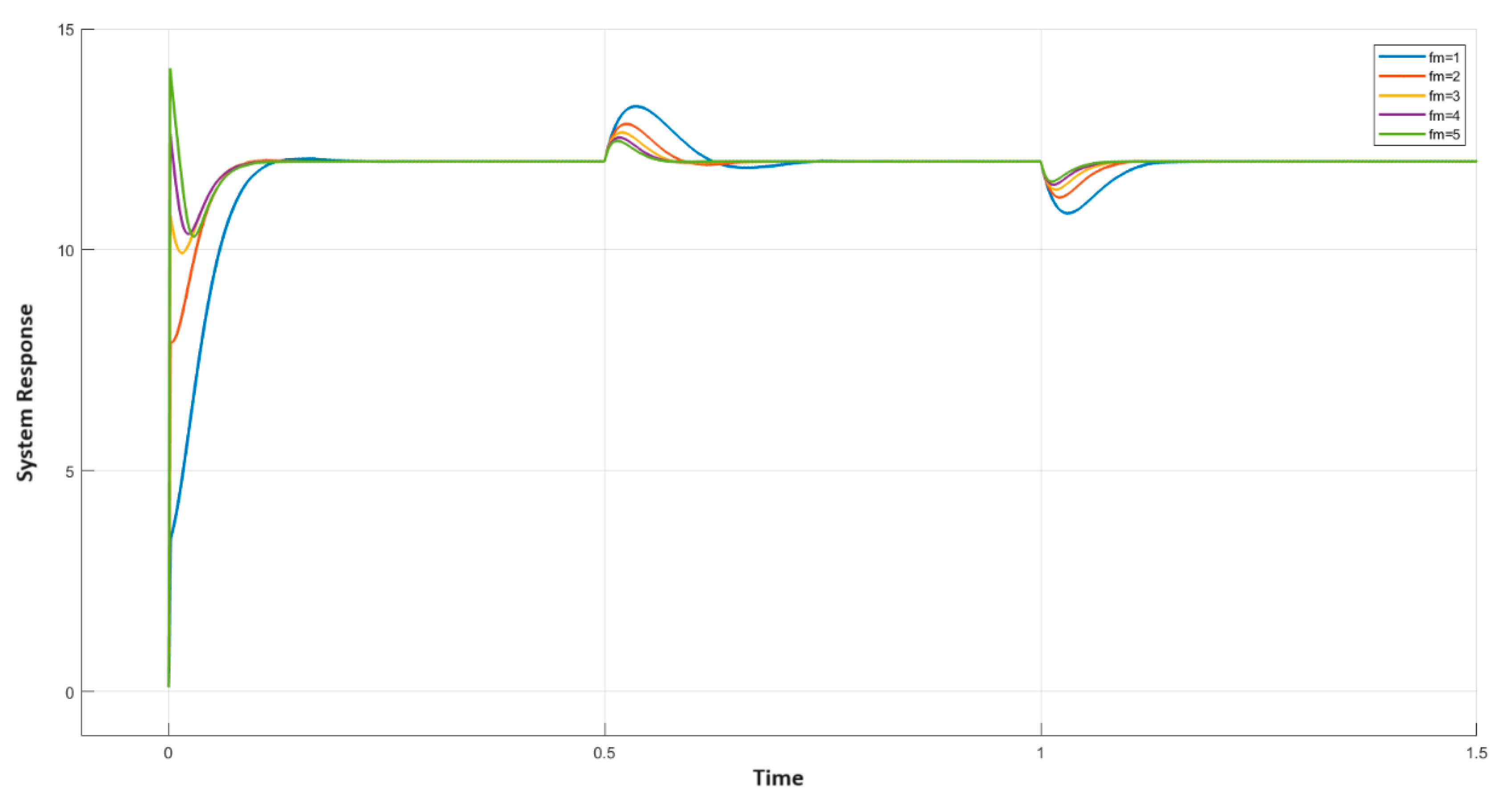
Next, the result of varying
on the response was studied and the other parameters
,
, and
were set to 0.1, 0.1, and 5, respectively. The load-change response for varying
from 1 to 5 was plotted in
Figure 10. It can be seen that as
increases, the transient response’s overshoot increases but the load change response’s settling time reduces significantly. Thus, a medium value of
should be chosen to achieve a better quality of the output curve.
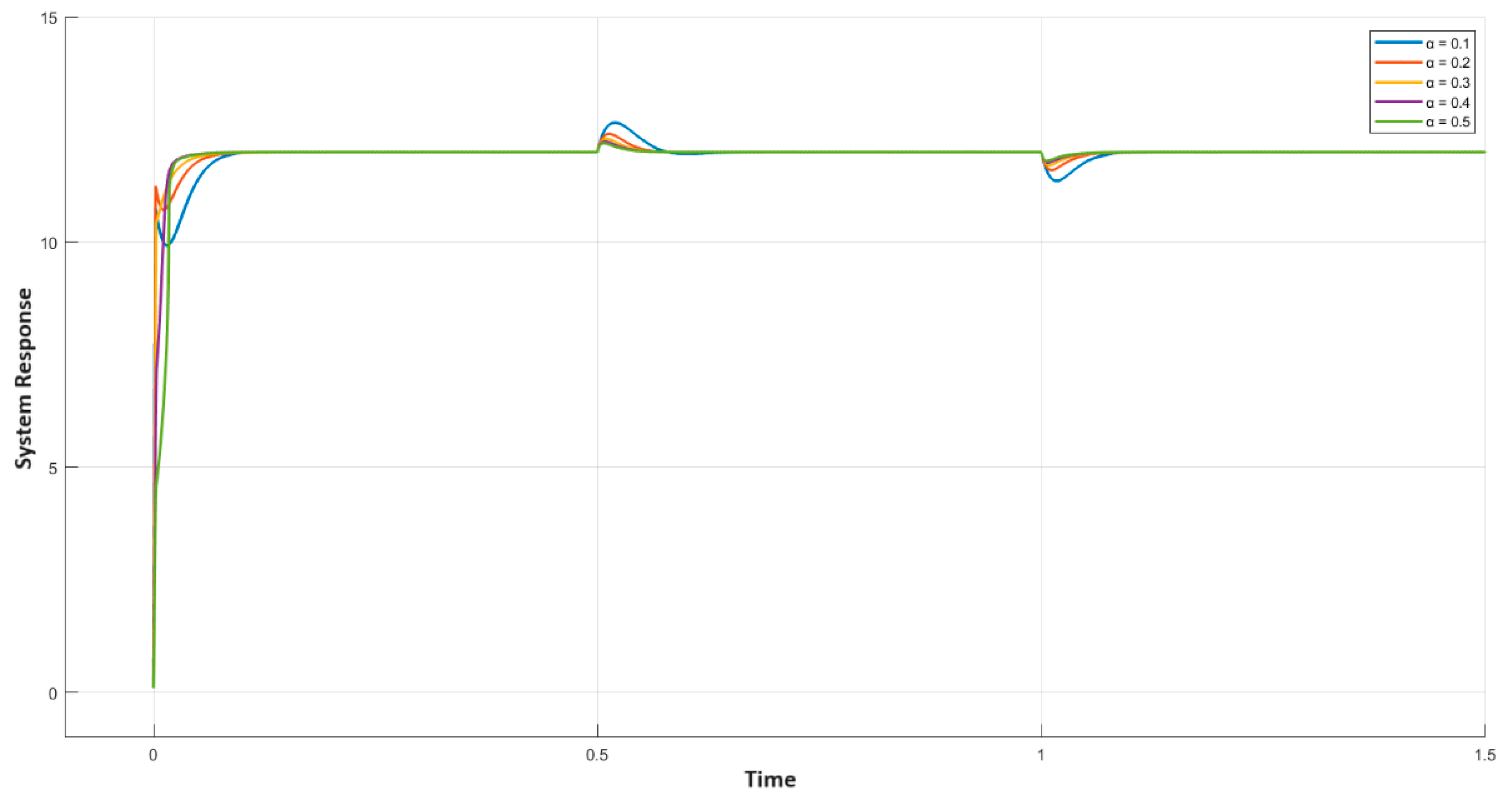
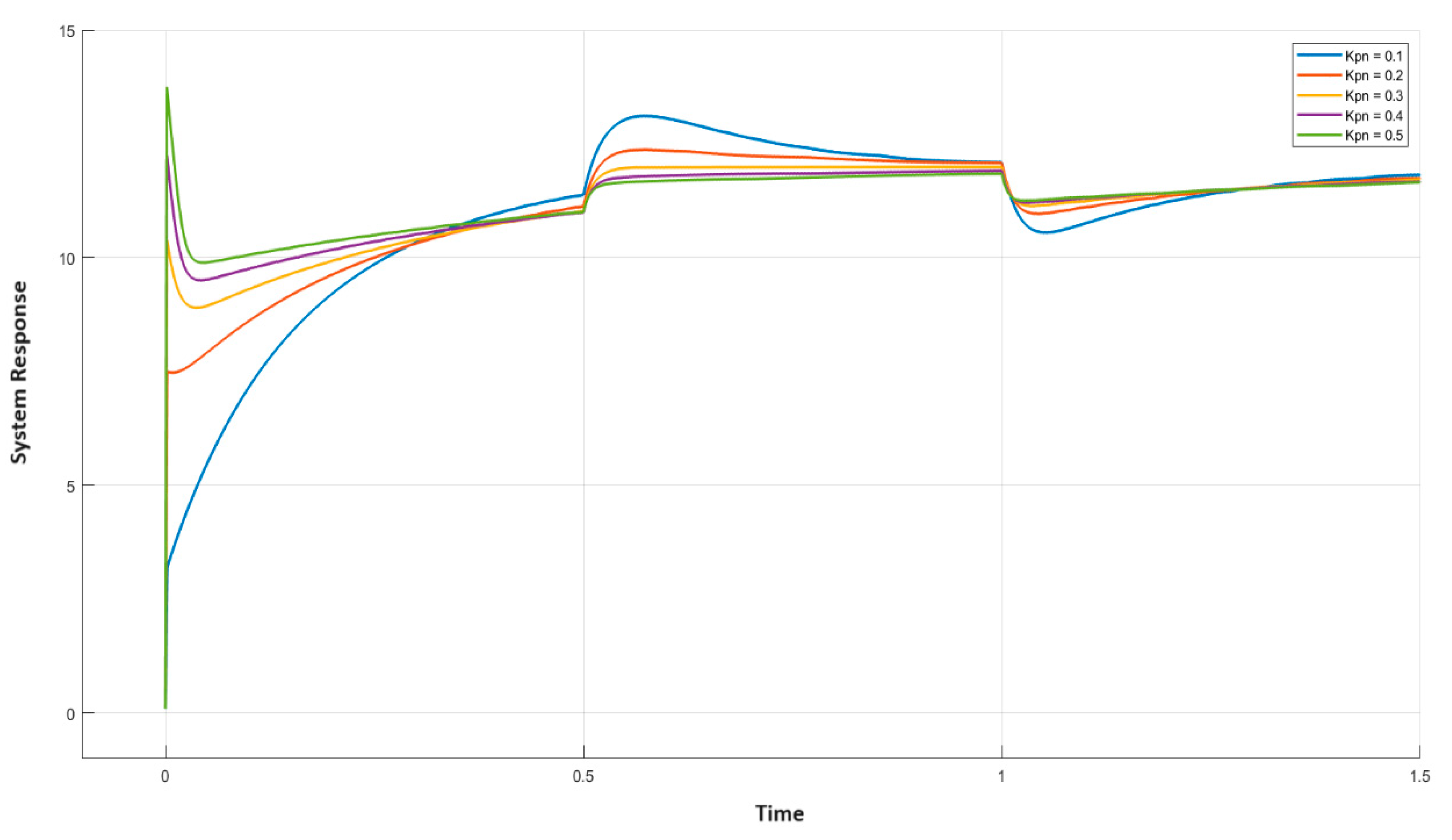
Finally, the consequence of varying
on the load response was explored and other parameters
,
, and
were set to 0.1, 3, and 5, respectively. The load-change response for varying
from 0.1 to 0.5 was plotted in
Figure 11. It can be seen that as
increases, both the overshoot and settling time of the load-change curve improve. Thus, a higher value of
is preferred.
Considering all this, the following values of controller parameters were chosen to authenticate the response of the closed-loop converter with the occurrence of load, line, and desired voltage variations.
- B.
Parameter variation Response
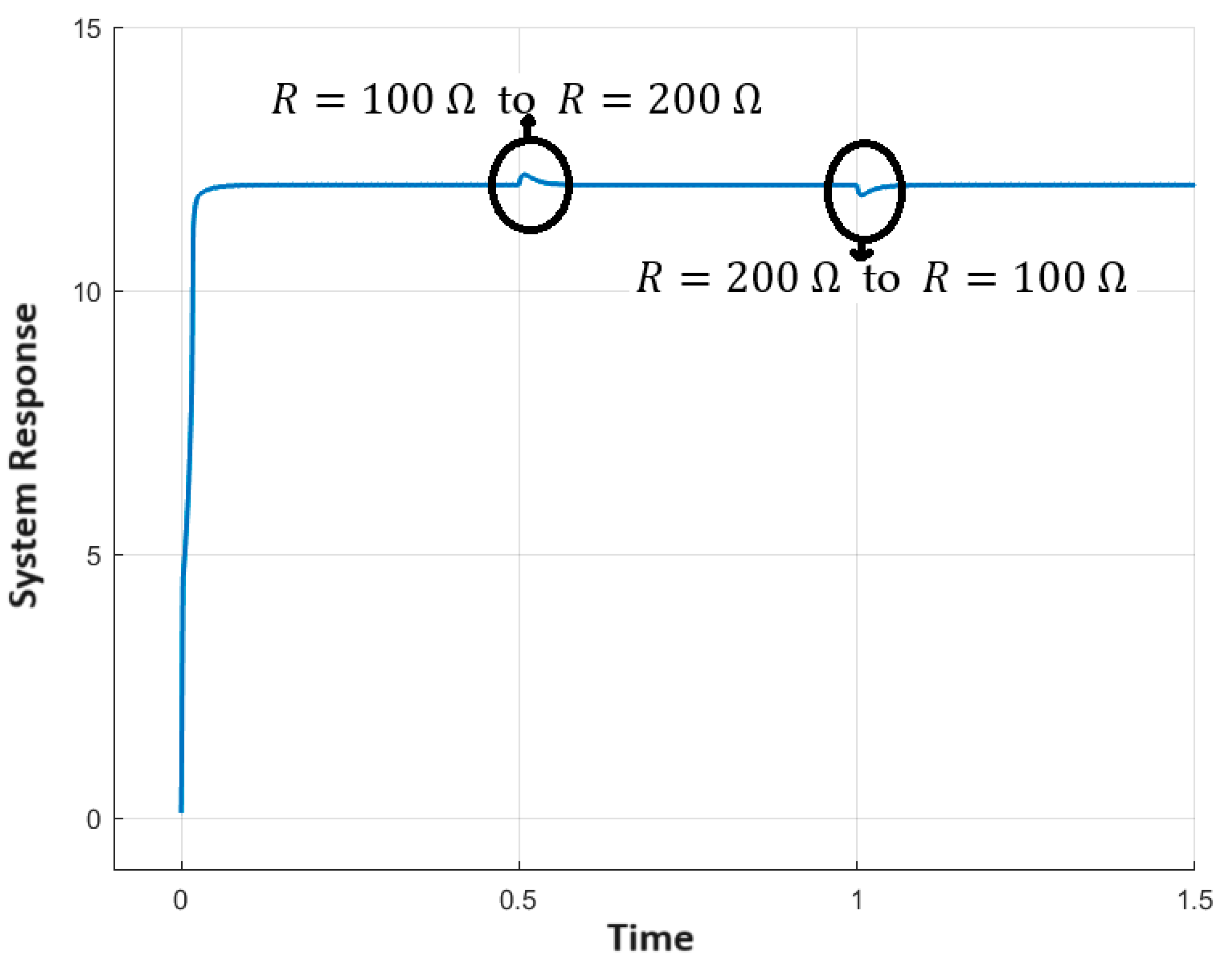
Next, the effect of different parameter variations on the response was analyzed.
Figure 12 shows the output curve for the load change when the resistance changed from
to
at time t = 1 s and was brought back to
at time t = 1.5 s. The overshoot of the load-change curve is ~1.6% and the settling time is ~0.06 s.
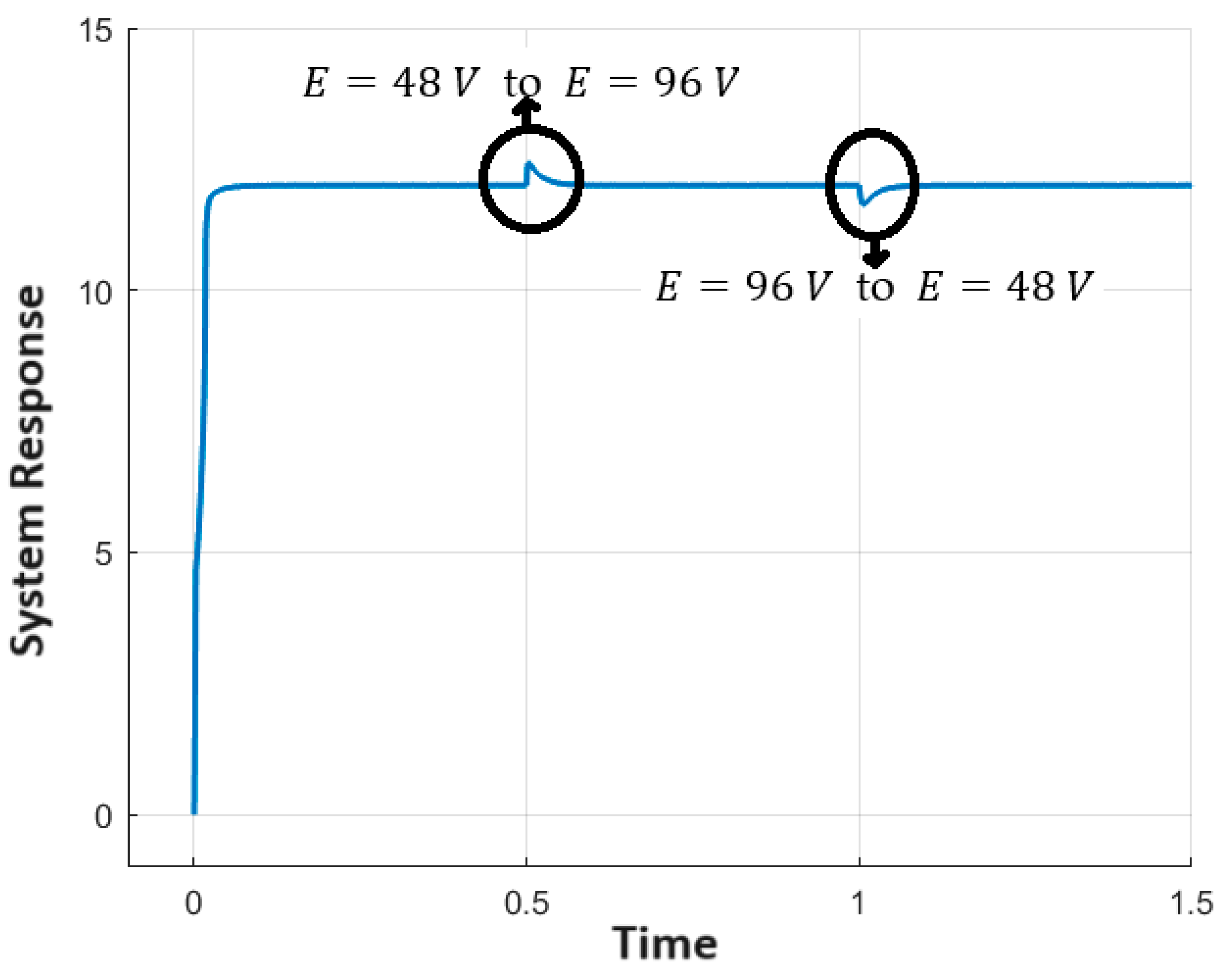
Next, the effect of varying the line voltage was checked.
Figure 13 depicts the input voltage variation response when the input was manipulated from its nominal value of
to
at time t = 1 s and bought again to
at time t = 1.5 s. Again, it was observed that the response immediately settled to the desired voltage along with an overshoot of ~3% and sa ettling time of ~0.06 s. Finally, the capability of the control scheme to handle desired voltage changes was explored.
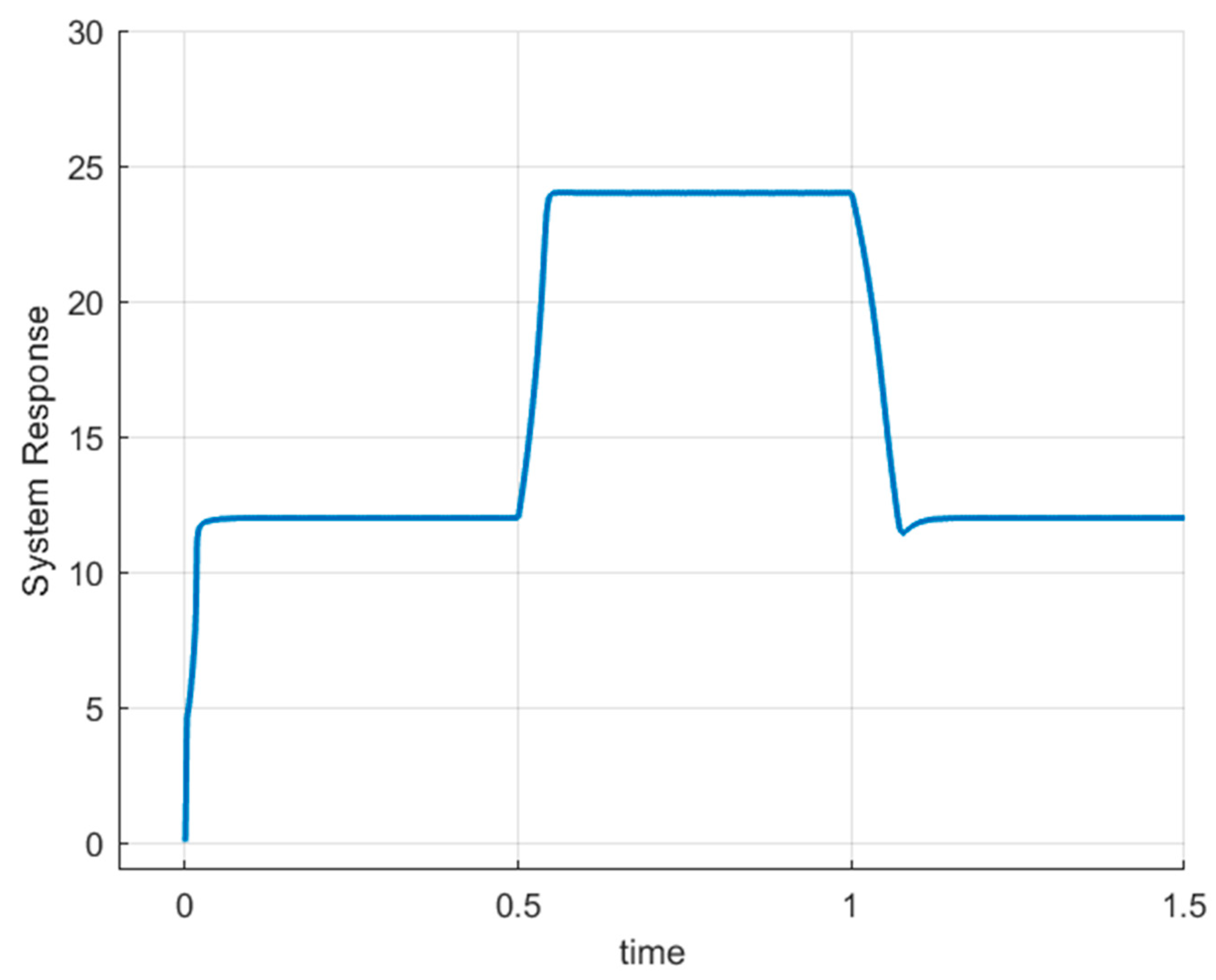
Figure 14 illustrates the line-change curve when the desired value was altered from
to
at time t = 1 s and again back to
at time t = 1.5 s. Again, the output successfully tracked the desired reference.
All of these findings attest to the suggested normalized error-based PI controller’s capability to control the step-down power converter.
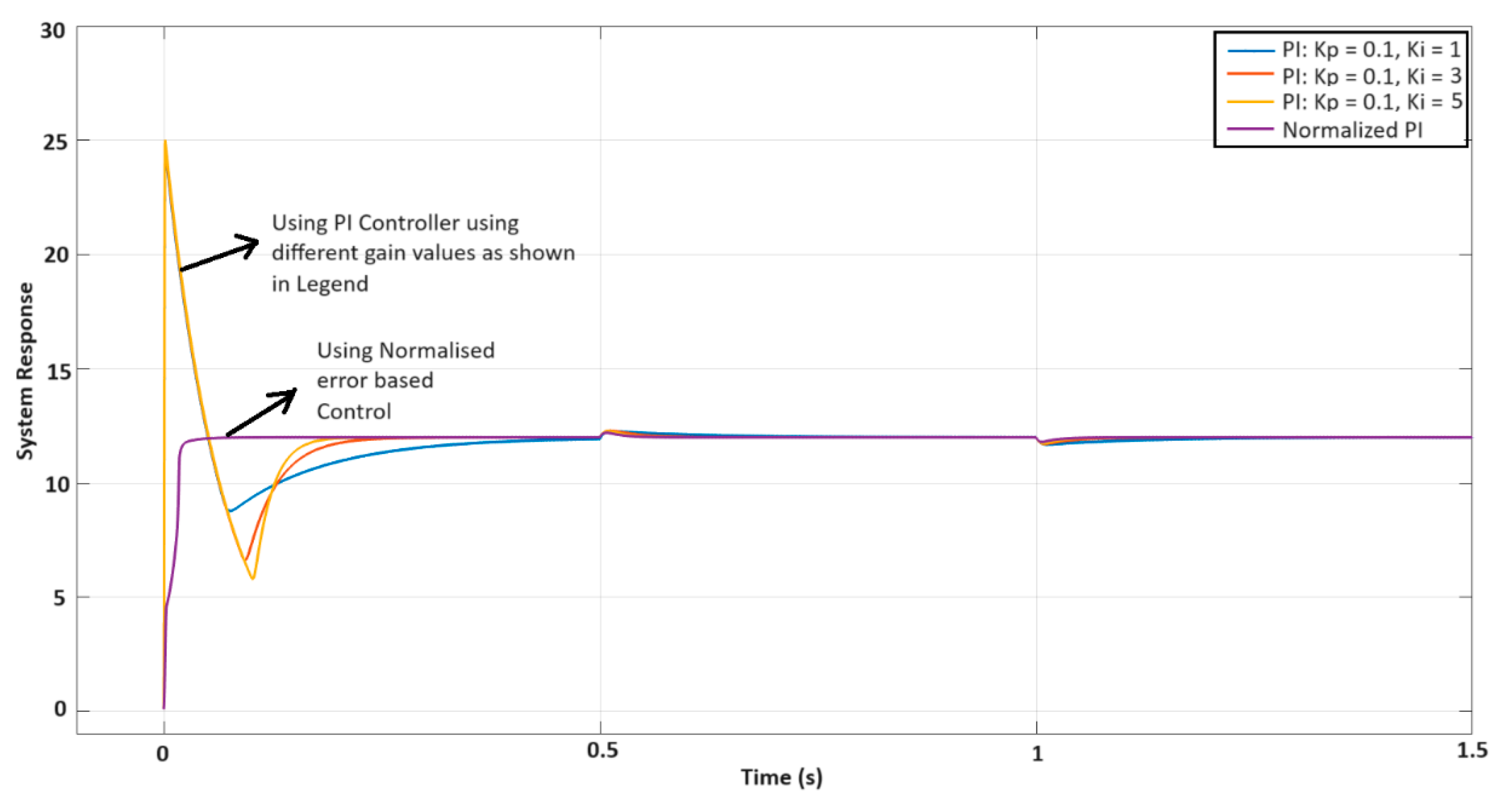
Lastly, to validate the theoretical conclusions, a comparative study of the widely used PI controller and the proposed normalized error-based controller was carried out.
Figure 15 shows the transient and load-change responses of the buck converter obtained using two controllers. The load was changed from 100 Ω to 200 Ω at time t = 1 s and bought back to 100 Ω at time t = 1.5 s. It can be observed that the initial overshoot of the transient response is higher when a PI controller is employed without any normalized error term. The superior performance of the proposed normalized error-based controller is evident from the transient response part of
Figure 15. The bounded integrand and thus bounded control signal (see
Figure 3) limits the overshoot in the transient response when the error signal is normalized. This validates the theoretical conclusions.


