
Influence of Homo- and Hetero-Junctions on the Propagation Characteristics of Radially Propagated Cylindrical Surface Acoustic Waves in a Piezoelectric Semiconductor Semi-Infinite Medium


Abstract
1. Introduction
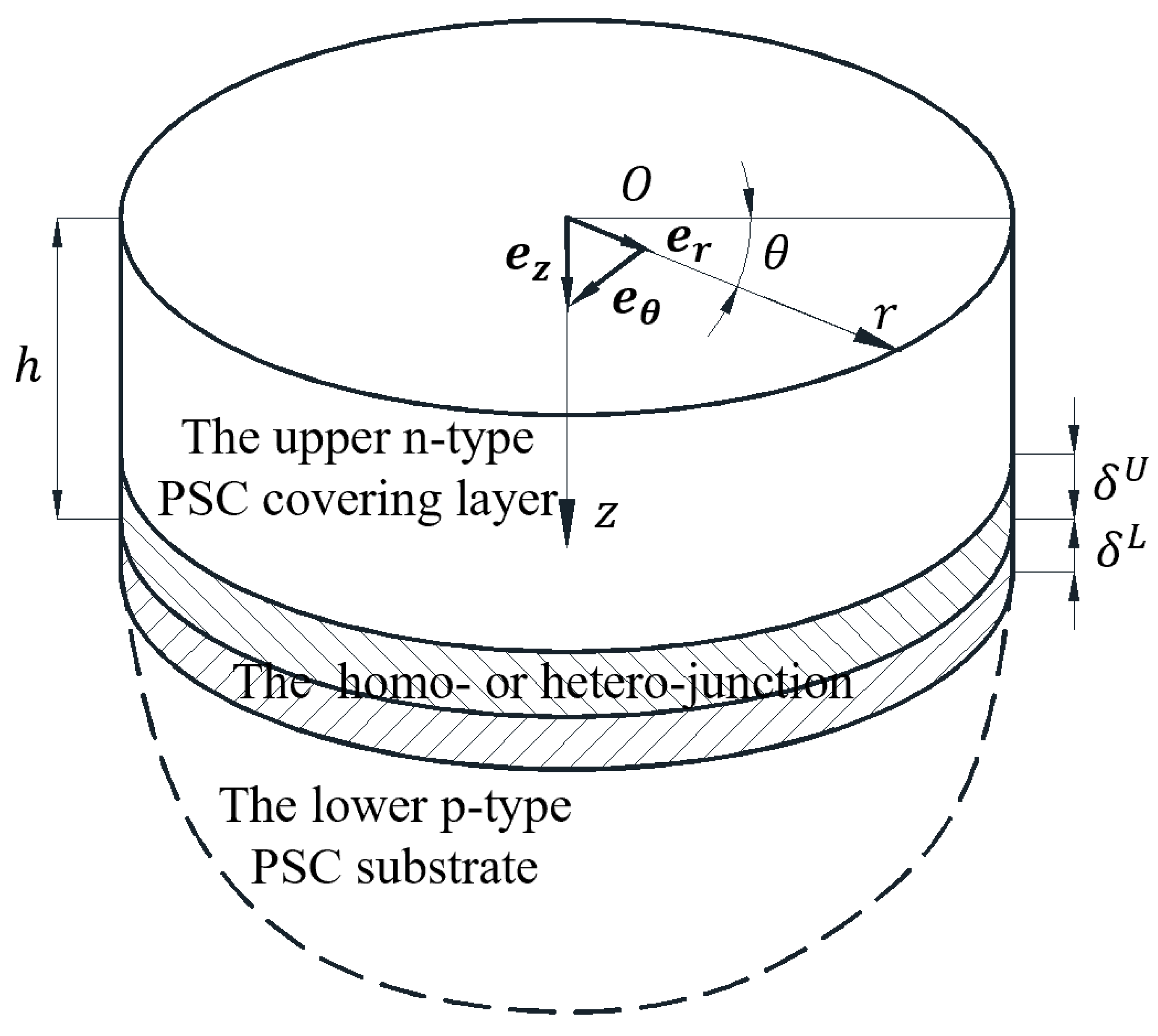
2. Problem Description and Basic Equations
3. Two Equivalent Mathematical Models
3.1. The First Mathematical Model
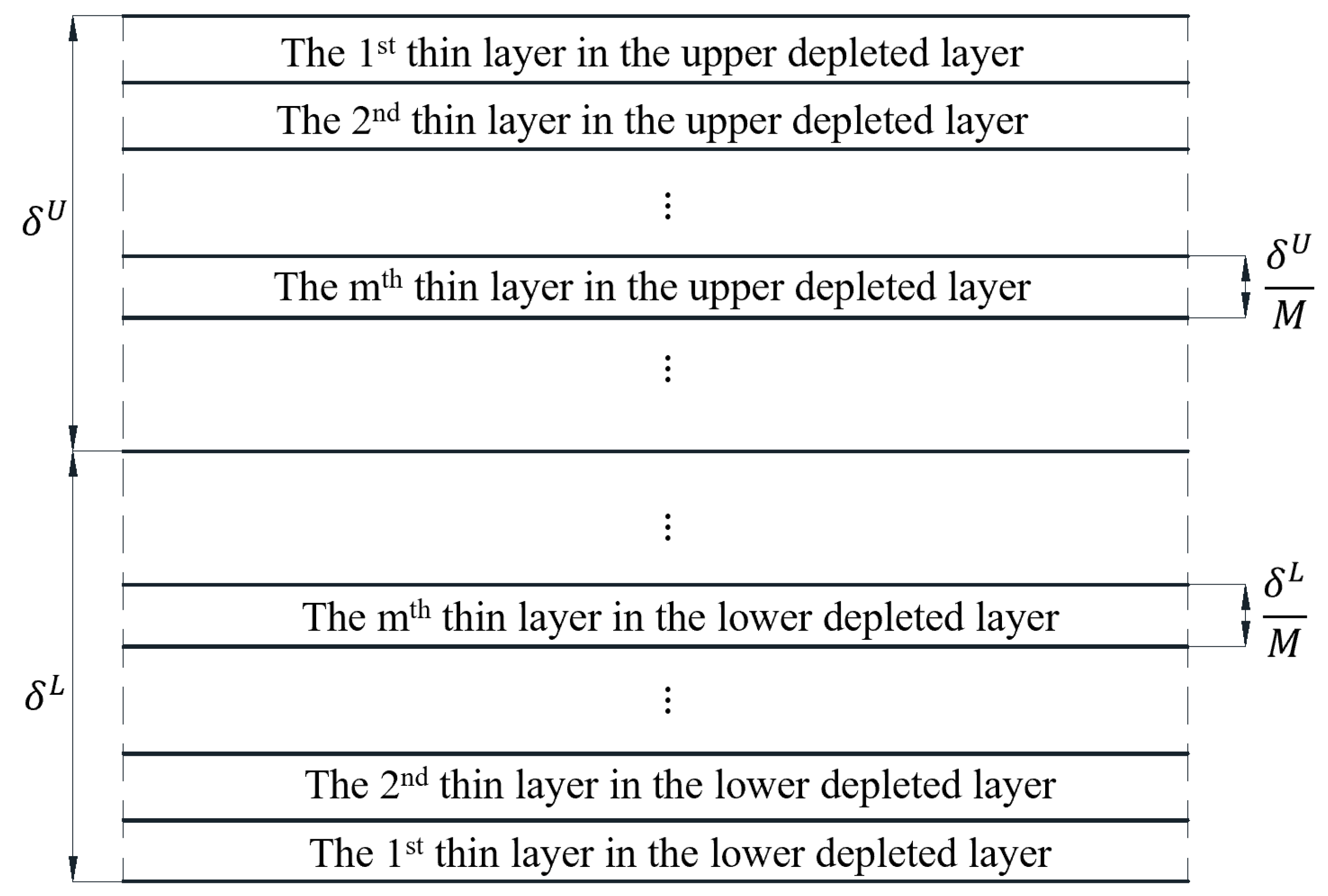
3.2. The Second Mathematical Model
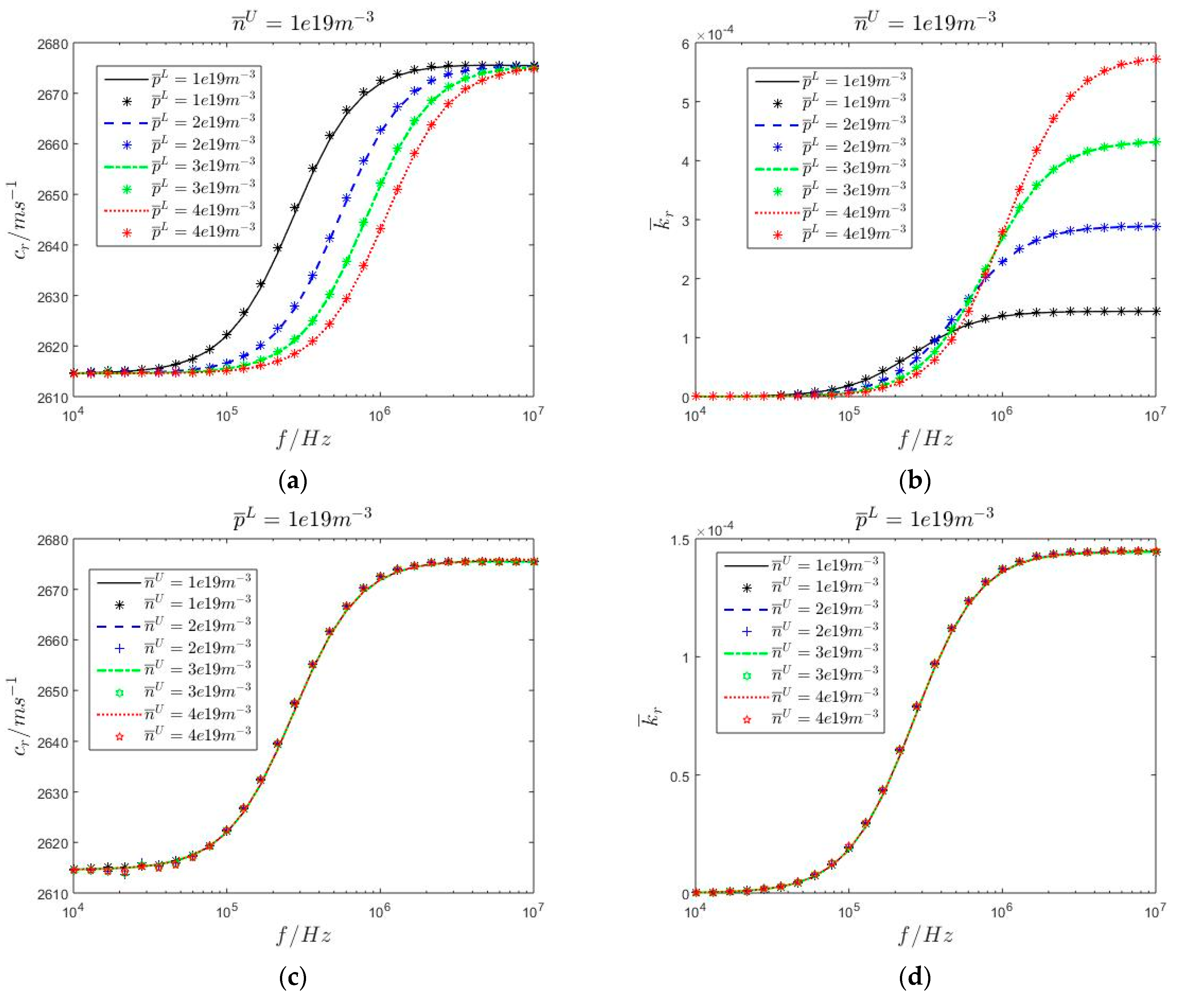
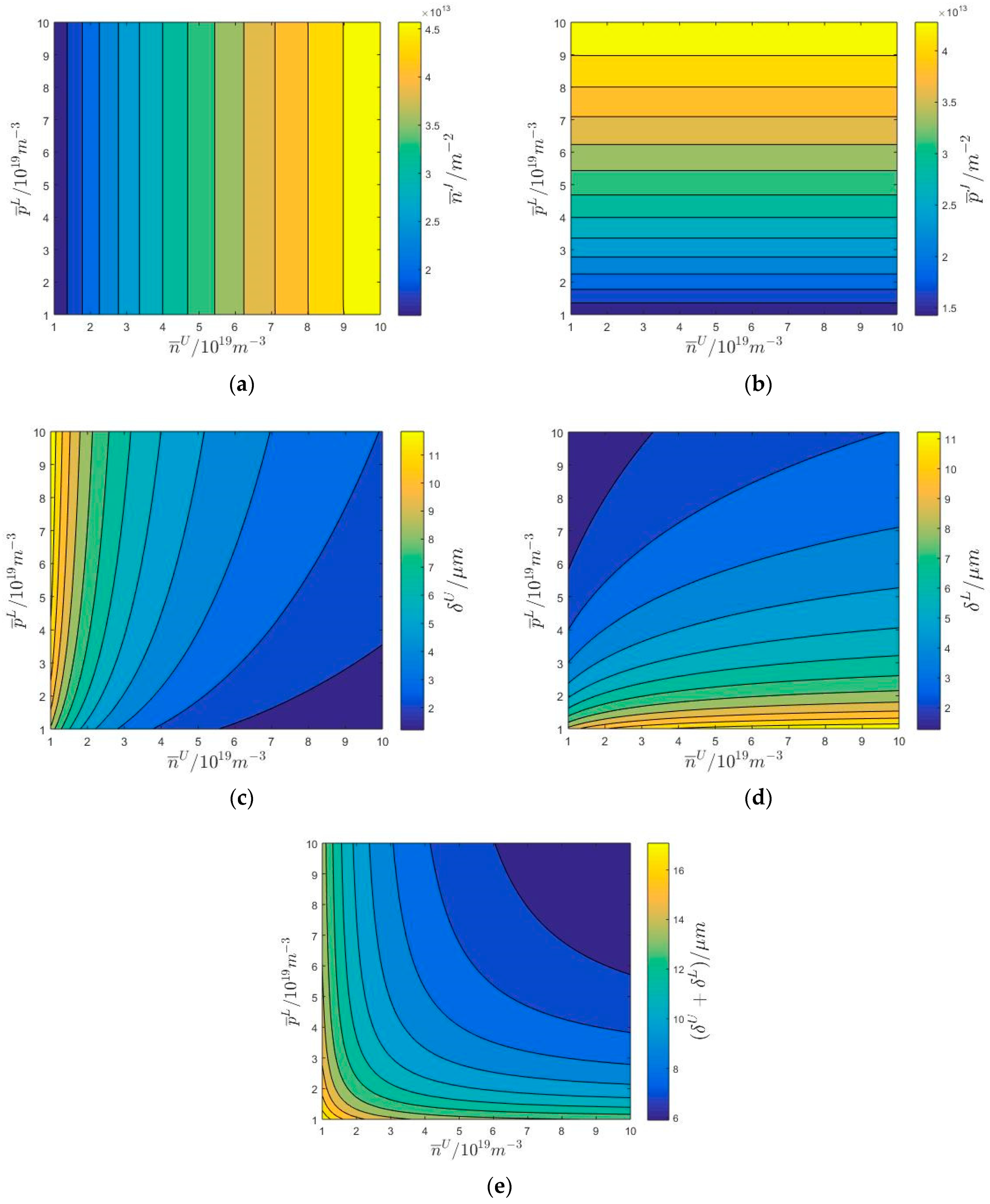
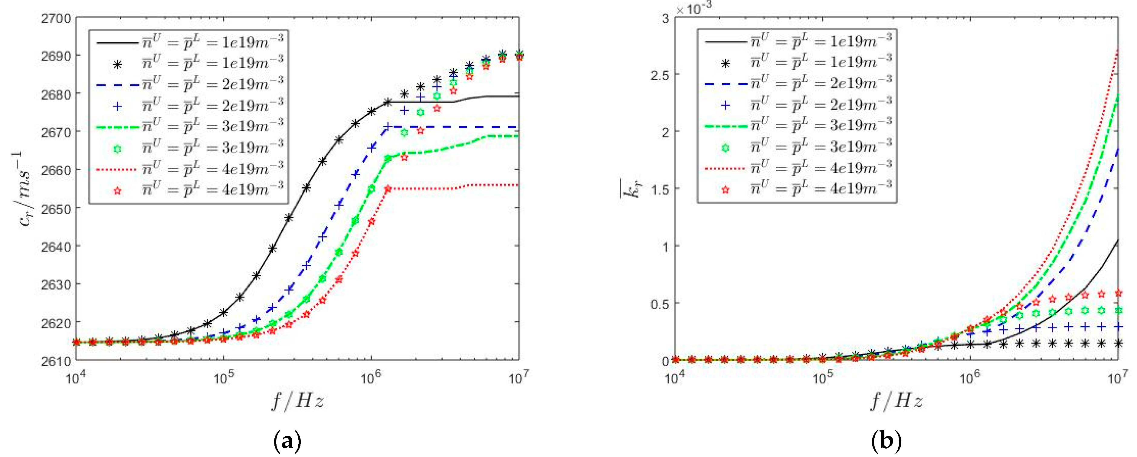
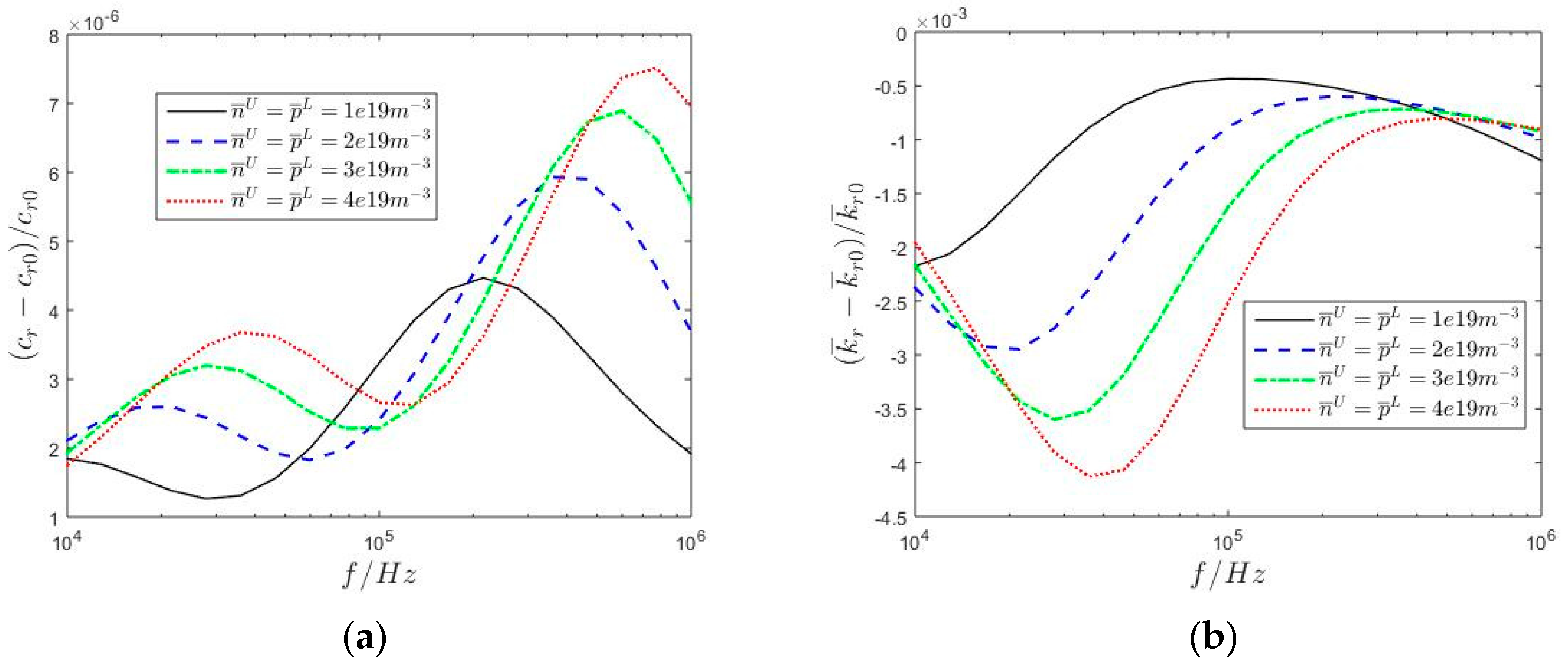
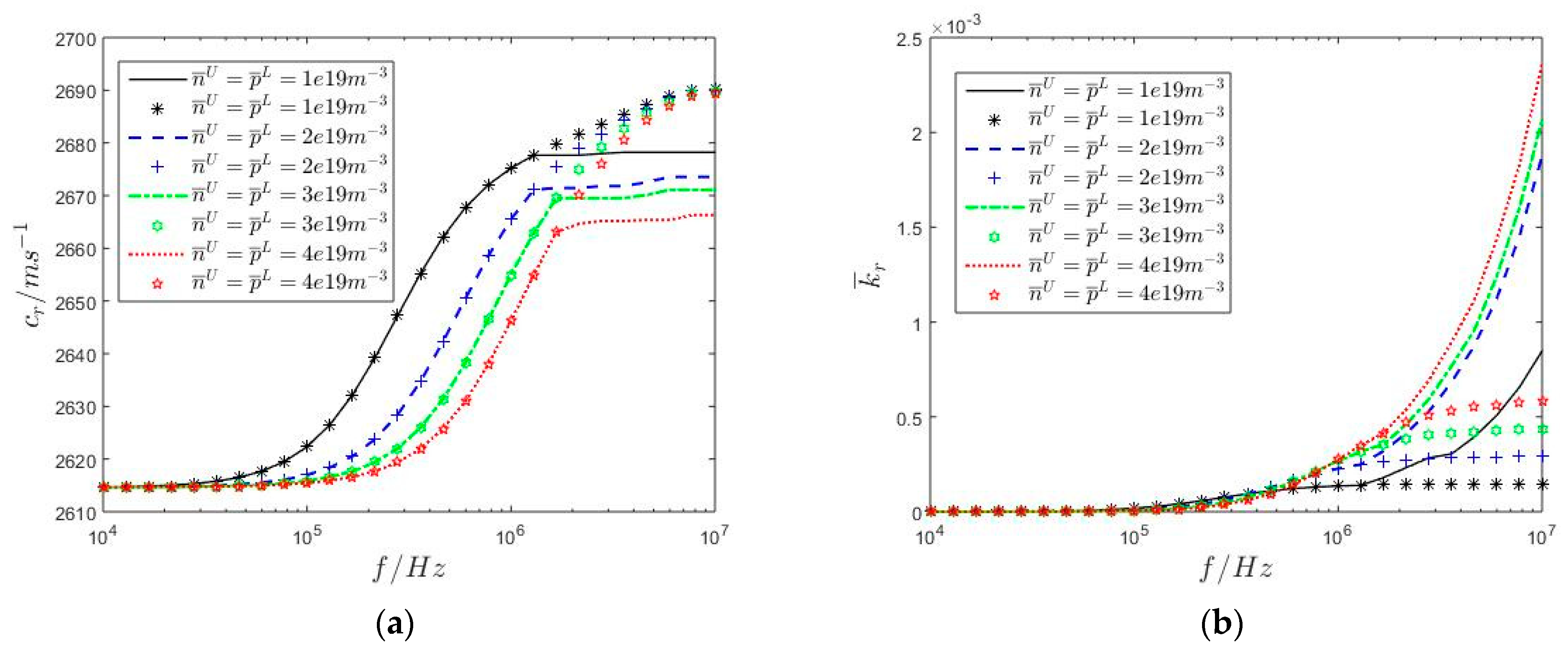
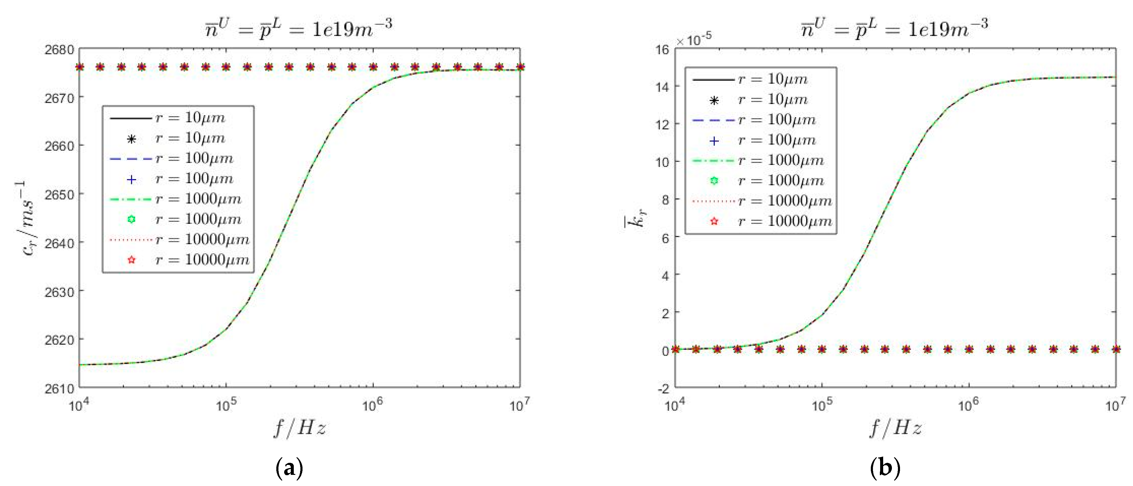
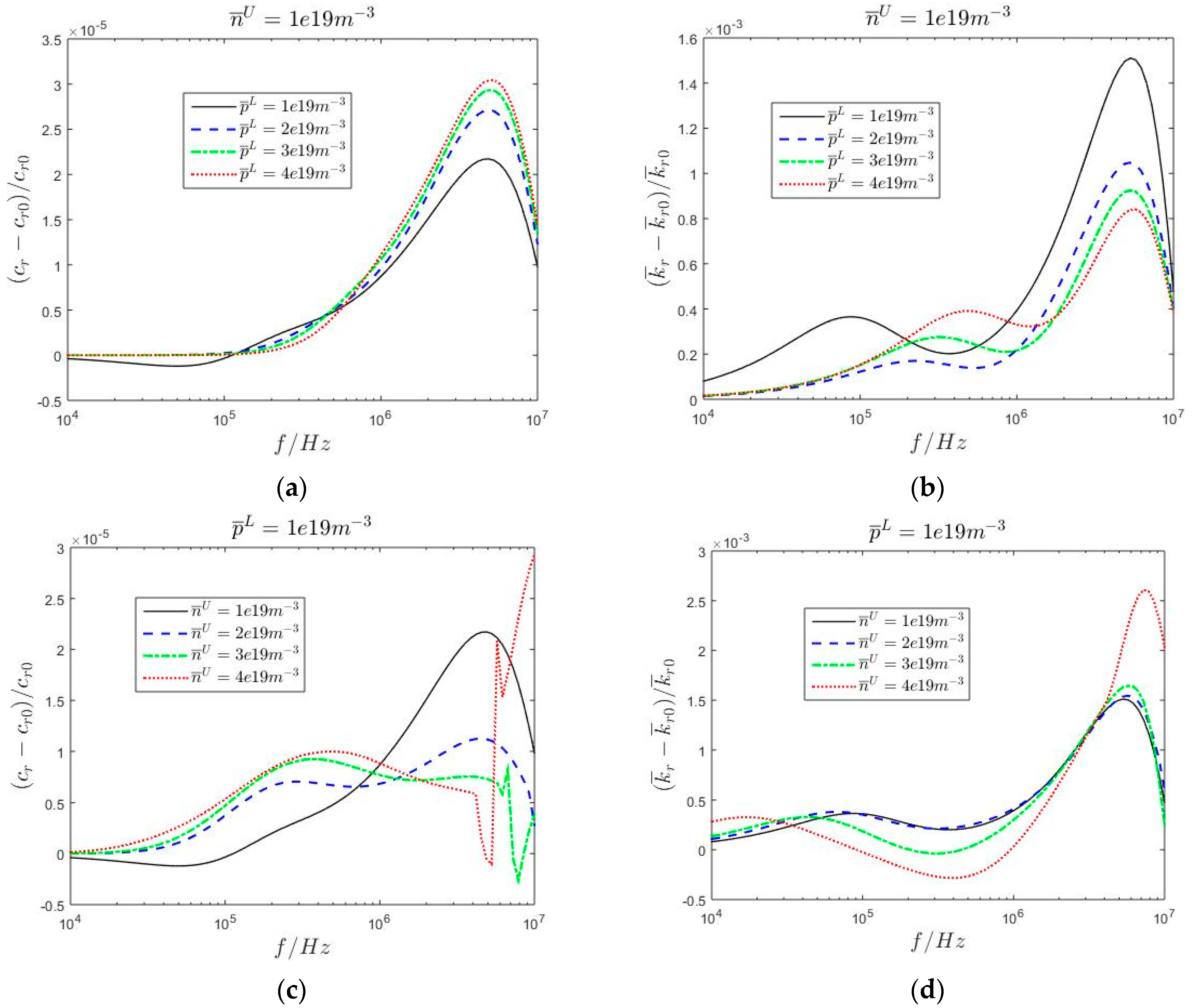
4. Numerical Results and Discussion
5. Concluding Remarks
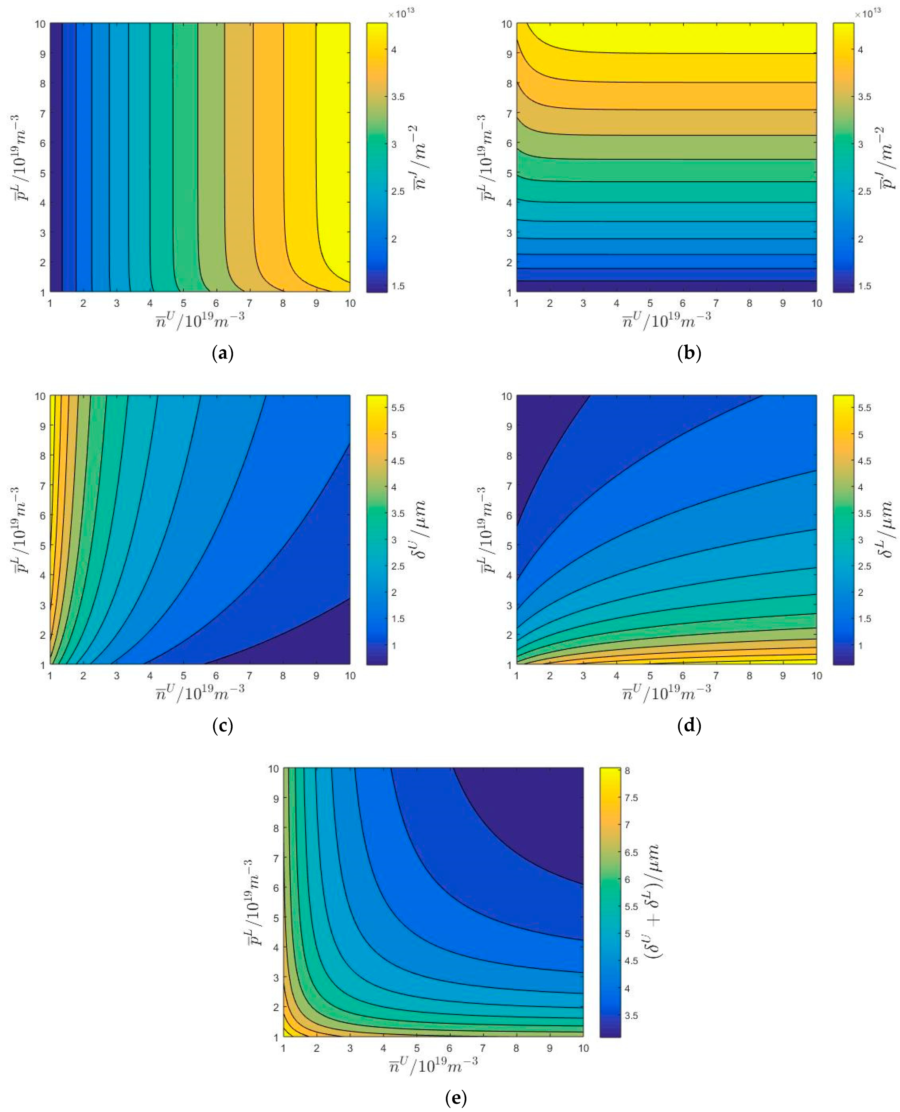
- The physical properties of the homo- and hetero-junctions are closely related to the doping modes and concentrations in the PSC semi-infinite medium, of which the increase not only makes the homo- and hetero-junctions more like electrically imperfect interfaces but also enhance the influence of the homo- and hetero-junctions.
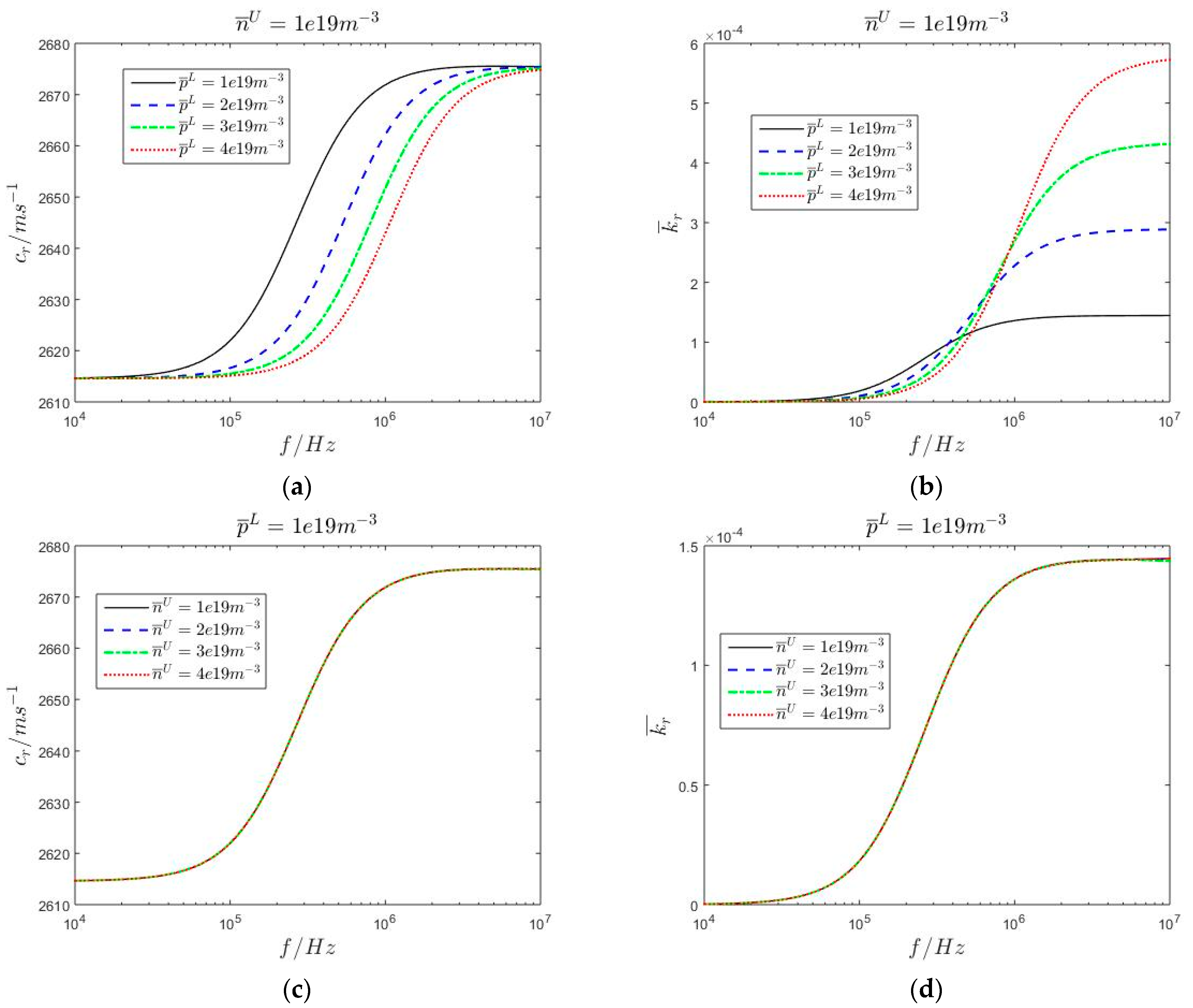
- The influence of the homo- and hetero-junctions on the dispersion and attenuation characteristics of radially propagated cylindrical SAW is closely related to the angular frequency. It is of great significance to consider the existence of homo- and hetero-junctions when studying the propagation of high-frequency SAW in PSC materials.
- The homo- and hetero-junctions can enhance the conversion efficiency from mechanical to electrical energy; adjusting doping modes and concentrations of PSC semi-infinite medium can regulate attenuation characteristics of cylindrical SAW and optimize the acoustic characteristics of SAW resonators, energy harvesters, and acoustic wave amplification formed by PSC semi-infinite medium.
- Since the dispersion and attenuation characteristics of cylindrical SAW are independent of the radial coordinate, the mathematical models in this paper provide theoretical guidance for studying the propagation characteristics of other types of SAW in PSC materials, such as the Rayleigh-type SAW. Since the influence of the homo- and hetero-junctions mainly concentrates on the attenuation characteristic of SAW, the discussion in this paper provides theoretical guidance for the design and manufacture of SAW resonators [3,4], energy harvesting [6,7], and acoustic wave amplification [8]. Due to the interface characteristic lengths, the first mathematical model is more complex than the second. The homo- and hetero-junctions are treated as functional gradient thin layers; the second mathematical model is more accurate than the first. Based on Figure 9 and Figure 11, the computational stability of the second mathematical model is weaker than that of the first. Considering the interface characteristic lengths are independent of the doping concentrations, the first mathematical model is more practical in studying wave motion problems. Based on Figure 6 and Figure 10, the relative changes of the radial wave speed and dimensionless attenuation coefficient are considerably lower than 1, which means that the homo- and hetero-junctions have less evident influence on the propagation characteristics of low-frequency radially propagated cylindrical SAW. Therefore, in subsequent work, we must establish a simpler mathematical model with better computational accuracy and stability to study the propagation characteristics of high-frequency SAW in the PSC materials, such as the PSC layered composite structures containing multi-layer homo- and hetero-junctions.
Author Contributions
Funding
Data Availability Statement
Conflicts of Interest
Appendix A
References
- Patel, R.; Patel, M.; Boolchandani, D.; Rangra, K. FEM modeling of solidly mounted film bulk acoustic resonator and gas sensor using PIB-sensitive layer. J. Micro/Nanolithogr. MEMS MOEMS 2017, 16, 025002. [Google Scholar] [CrossRef]
- Wang, J.; Park, M.; Mertin, S.; Pensala, T.; Ayazi, F.; Ansari, A. A film bulk acoustic resonator based on ferroelectric aluminum scandium nitride films. J. Microelectromech. Syst. 2020, 29, 741–747. [Google Scholar] [CrossRef]
- Patel, R.; Adhikari, M.S.; Boolchandani, D. Active area optimisation of film bulk acoustic resonator for improving performance parameters. Electron. Lett. 2020, 56, 1191–1194. [Google Scholar] [CrossRef]
- Hu, Y.; Dong, B.; Lei, L.; Wang, Z.; Ruan, S. High-order harmonic film bulk acoustic resonator based on a polymer reflector. Sensors 2022, 22, 7439. [Google Scholar] [CrossRef] [PubMed]
- Lv, L.; Shuai, Y.; Bai, X.; Huang, S.; Zhu, D.; Wang, Y.; Zhao, J.; Luo, W.; Wu, C.; Zhang, W. wide band BAW filter based on single-crystalline linbo3; thin film with insulating bragg reflector. IEEE Trans. Ultrason. Ferroelectr. Freq. Control. 2022, 69, 1535–1541. [Google Scholar] [CrossRef] [PubMed]
- Kumar, B.; Kim, S.W. Energy harvesting based on semiconducting piezoelectric ZnO nanostructures. Nano Energy 2012, 1, 342–355. [Google Scholar] [CrossRef]
- Hiralal, P.; Unalan, H.E.; Amaratunga, G.A.J. Nanowires for energy generation. Nanotechnology 2012, 23, 194002. [Google Scholar] [CrossRef] [PubMed]
- Fan, J.C.; Sreekanth, K.M.; Xie, Z.; Chang, S.L.; Rao, K.V. P-type ZnO materials: Theory, growth, properties and devices. Prog. Mater. Sci. 2013, 58, 874–985. [Google Scholar] [CrossRef]
- Gurtin, M.E.; Ian Murdoch, A. A continuum theory of elastic material surfaces. Arch. Ration. Mech. Anal. 1975, 57, 291–323. [Google Scholar] [CrossRef]
- Murdoch, A.I. The propagation of surface waves in bodies with material boundaries. J. Mech. Phys. Solids 1976, 24, 137–146. [Google Scholar] [CrossRef]
- Gurtin, M.E.; Ian Murdoch, A. Surface stress in solids. Int. J. Solids Struct. 1978, 14, 431–440. [Google Scholar] [CrossRef]
- Chen, W. Surface effect on Bleustein-Gulyaev wave in a piezoelectric substrate. Theor. Appl. Mech. Lett. 2011, 1, 041001. [Google Scholar] [CrossRef]
- Zhang, L.L.; Liu, J.X.; Fang, X.Q.; Nie, G.Q. Effects of surface piezoelectricity and nonlocal scale on wave propagation in piezoelectric nanoplates. Eur. J. Mech.—A/Solids 2014, 46, 22–29. [Google Scholar] [CrossRef]
- Zhang, L.L.; Liu, J.X.; Fang, X.Q.; Nie, G.Q. Size-dependent dispersion characteristics in piezoelectric nanoplates with surface effects. Phys. E Low-Dimens. Syst. Nanostruct. 2014, 57, 169–174. [Google Scholar] [CrossRef]
- Zhang, S.; Gu, B.; Zhang, H.; Feng, X.Q.; Pan, R.; Alamusi; Hu, N. Propagation of Love waves with surface effects in an electrically-shorted piezoelectric nanofilm on a half-space elastic substrate. Ultrasonics 2016, 66, 65–71. [Google Scholar] [CrossRef] [PubMed]
- Zhang, L.L.; Zhao, J.; Liu, X.L.; Liu, J.X. Shear horizontal surface waves in piezoelectric materials with surface stress. Philos. Mag. Lett. 2018, 98, 350–357. [Google Scholar] [CrossRef]
- Enzevaee, C.; Shodja, H.M. Crystallography and surface effects on the propagation of Love and Rayleigh surface waves in fcc semi-infinite solids. Int. J. Solids Struct. 2018, 138, 109–117. [Google Scholar] [CrossRef]
- Qian, J.; Lia, C.; Qian, L.; Lia, M.; Li, H.; Yang, B. Three-dimensional finite element simulation of Love mode surface acoustic wave in layered structures including ZnO piezoelectric film and diamond substrate. Diam. Relat. Mater. 2018, 88, 123–128. [Google Scholar] [CrossRef]
- Zhu, F.; Pan, E.; Qian, Z.; Wang, Y. Dispersion curves, mode shapes, stresses and energies of SH and Lamb waves in layered elastic nanoplates with surface/interface effect. Int. J. Eng. Sci. 2019, 142, 170–184. [Google Scholar] [CrossRef]
- Wang, X.; Li, P.; Jin, F. A generalized dynamic model of nanoscale surface acoustic wave sensors and its applications in Love wave propagation and shear-horizontal vibration. Appl. Math. Model. 2019, 75, 101–115. [Google Scholar] [CrossRef]
- Zhang, Y.; Liu, Y.; Wang, Z.L. Fundamental Theory of Piezotronics. Adv. Mater. 2011, 23, 3004–3013. [Google Scholar] [CrossRef] [PubMed]
- Fan, S.; Liang, Y.; Xie, J.; Hu, Y. Exact solutions to the electromechanical quantities inside a statically-bent circular ZnO nanowire by taking into account both the piezoelectric property and the semiconducting performance: Part I–Linearized analysis. Nano Energy 2017, 40, 82–87. [Google Scholar] [CrossRef]
- Fan, S.; Yang, W.; Hu, Y. Adjustment and control on the fundamental characteristics of a piezoelectric PN junction by mechanical-loading. Nano Energy 2018, 52, 416–421. [Google Scholar] [CrossRef]
- Liang, Y.; Fan, S.; Chen, X.; Hu, Y. Nonlinear effect of carrier drift on the performance of an n-type ZnO nanowire nanogenerator by coupling piezoelectric effect and semiconduction. Beilstein J. Nanotechnol. 2018, 9, 1917–1925. [Google Scholar] [CrossRef] [PubMed]
- Cao, X.; Hu, S.; Liu, J.; Shi, J. Generalized Rayleigh surface waves in a piezoelectric semiconductor substrate. Meccanica 2019, 54, 271–281. [Google Scholar] [CrossRef]
- Xu, C.; Wei, P.; Wei, Z.; Guo, X. Rayleigh wave in layered piezoelectric semiconductor with consideration of PN junction effects. Math. Mech. Solids 2023, 28, 1817–1833. [Google Scholar] [CrossRef]
- Tian, R.; Liu, J.; Pan, E.; Wang, Y.; Soh, A.K. Some characteristics of elastic waves in a piezoelectric semiconductor plate. J. Appl. Phys. 2019, 126, 125701. [Google Scholar] [CrossRef]
- Tian, R.; Liu, J.; Pan, E.; Wang, Y. SH waves in multilayered piezoelectric semiconductor plates with imperfect interfaces. Eur. J. Mech./A Solids 2020, 81, 103961. [Google Scholar] [CrossRef]
- Xu, C.; Wei, P.; Wei, Z.; Guo, X. Shear horizontal wave in a p-type Si substrate covered with a piezoelectric semiconductor n-type ZnO layer with consideration of PN heterojunction effects. Acta Mech. 2023. [Google Scholar] [CrossRef]
- Guo, X.; Wei, P. Dispersion relations of in-plane elastic waves in nano-scale one dimensional piezoelectric semiconductor/piezoelectric dielectric phononic crystal with the consideration of interface effect. Appl. Math. Model. 2021, 96, 189–214. [Google Scholar] [CrossRef]
- Guo, X.; Wei, P.; Xu, M.; Lan, M. Dispersion relations of anti-plane elastic waves in micro-scale one dimensional piezoelectric semiconductor phononic crystals with the consideration of interface effect. Mech. Mater. 2021, 161, 104000. [Google Scholar] [CrossRef]
- Chattopadhyay, A.; Gupta, S.; Sahu, S.A.; Dhua, S. Torsional surface waves in heterogeneous anisotropic substrate under initial stress. Arch. Appl. Mech. 2012, 83, 357–366. [Google Scholar] [CrossRef]
- Chattopadhyay, A.; Gupta, S.; Kumari, P.; Sharma, V.K. Torsional wave propagation in non-homogeneous layer between non-homogeneous substrates. Int. J. Numer. Anal. Methods Geomech. 2013, 37, 1280–1291. [Google Scholar] [CrossRef]
- Gupta, S.; Majhi, D.K.; Kundu, S.; Vishwakarma, S.K. Propagation of torsional surface waves in a homogeneous layer of finite thickness over an initially stressed heterogeneous substrate. Appl. Math. Comput. 2012, 218, 5655–5664. [Google Scholar]
- Gupta, S.; Majhi, D.K.; Vishwakarma, S.K. Torsional surface wave propagation in an initially stressed non-homogeneous layer over a non-homogeneous substrate. Appl. Math. Comput. 2012, 219, 3209–3218. [Google Scholar]
- Singh, A.K.; Lakshman, A. Effect of loosely bonded undulated boundary surfaces of doubly layered substrate on the propagation of torsional wave. Mech. Res. Commun. 2016, 73, 91–106. [Google Scholar] [CrossRef]
- Gupta, A.K.; Kundu, S.; Patra, P.; Mukhopadhyay, A.K. Effect of gravity and initial stresses on torsional surface waves in dry sandy medium under rigid layer. Procedia Eng. 2017, 173, 1042–1047. [Google Scholar] [CrossRef]
- Sultana, R.; Gupta, S. Torsional Wave Propagation in a sandy layer under initial stress over an inhomogeneous substrate. Procedia Eng. 2017, 173, 1003–1013. [Google Scholar] [CrossRef]
- Enzevaee, C.; Shodja, H.M. Torsional surface wave propagation in a transversely isotropic FG substrate with piezoelectric over-layer within surface/interface theory. Acta Mech. 2020, 231, 2203–2216. [Google Scholar] [CrossRef]
- Zhang, Z.; Wen, Z.; Wang, C. Investigation of surface acoustic waves propagating in ZnO–SiO2–Si multilayer structure. Ultrasonics 2013, 53, 363–368. [Google Scholar] [CrossRef]


| ZnO | |||||||||||||||
| GaN | |||||||||||||||
| ZnO | |||||||||||||||
| GaN | |||||||||||||||
Disclaimer/Publisher’s Note: The statements, opinions and data contained in all publications are solely those of the individual author(s) and contributor(s) and not of MDPI and/or the editor(s). MDPI and/or the editor(s) disclaim responsibility for any injury to people or property resulting from any ideas, methods, instructions or products referred to in the content. |
© 2024 by the authors. Licensee MDPI, Basel, Switzerland. This article is an open access article distributed under the terms and conditions of the Creative Commons Attribution (CC BY) license (https://creativecommons.org/licenses/by/4.0/).
Share and Cite
Guo, X.; Wang, Y.; Xu, C.; Wei, Z.; Ding, C. Influence of Homo- and Hetero-Junctions on the Propagation Characteristics of Radially Propagated Cylindrical Surface Acoustic Waves in a Piezoelectric Semiconductor Semi-Infinite Medium. Mathematics 2024, 12, 145. https://doi.org/10.3390/math12010145
Guo X, Wang Y, Xu C, Wei Z, Ding C. Influence of Homo- and Hetero-Junctions on the Propagation Characteristics of Radially Propagated Cylindrical Surface Acoustic Waves in a Piezoelectric Semiconductor Semi-Infinite Medium. Mathematics. 2024; 12(1):145. https://doi.org/10.3390/math12010145
Chicago/Turabian StyleGuo, Xiao, Yilin Wang, Chunyu Xu, Zibo Wei, and Chenxi Ding. 2024. "Influence of Homo- and Hetero-Junctions on the Propagation Characteristics of Radially Propagated Cylindrical Surface Acoustic Waves in a Piezoelectric Semiconductor Semi-Infinite Medium" Mathematics 12, no. 1: 145. https://doi.org/10.3390/math12010145
APA StyleGuo, X., Wang, Y., Xu, C., Wei, Z., & Ding, C. (2024). Influence of Homo- and Hetero-Junctions on the Propagation Characteristics of Radially Propagated Cylindrical Surface Acoustic Waves in a Piezoelectric Semiconductor Semi-Infinite Medium. Mathematics, 12(1), 145. https://doi.org/10.3390/math12010145