
Mathematical Expressions Useful for Tunable Properties of Simple Square Wave Generators


Abstract
1. Introduction
- (a)
- introduction of two new and very simple solutions of electronically tunable generators employing single IC,
- (b)
- improvement of the tunability range and the tunability efficiency (ratio of the frequency range vs. the driving parameter range),
- (c)
- study of mathematical dependences of the frequency on the driving parameters and further consequences,
- (d)
- tests of tunability and efficiency for the nonlinear driving of the adjustable parameter,
- (e)
- comparison of expected and real (experimentally obtained) features of both circuits.
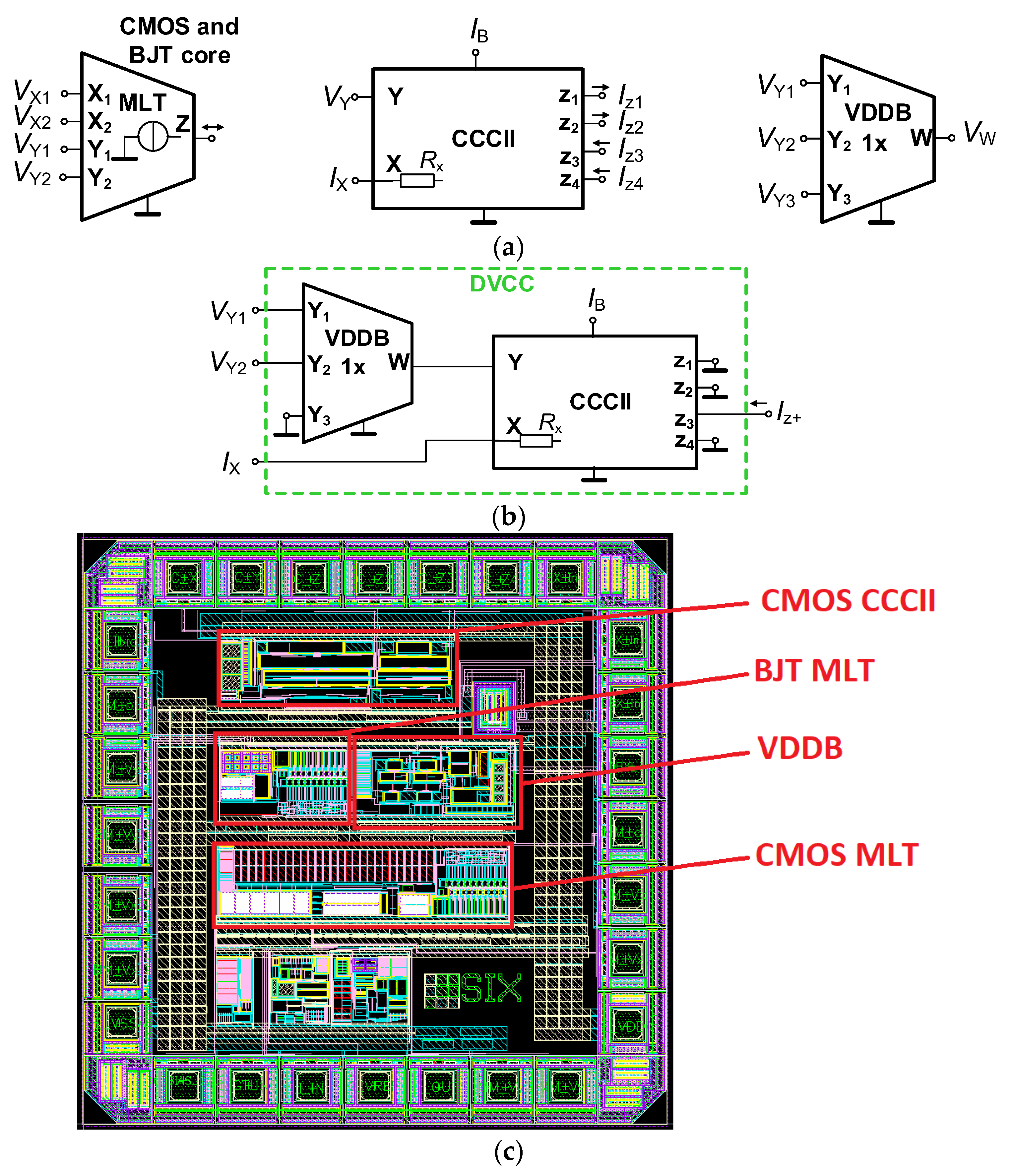
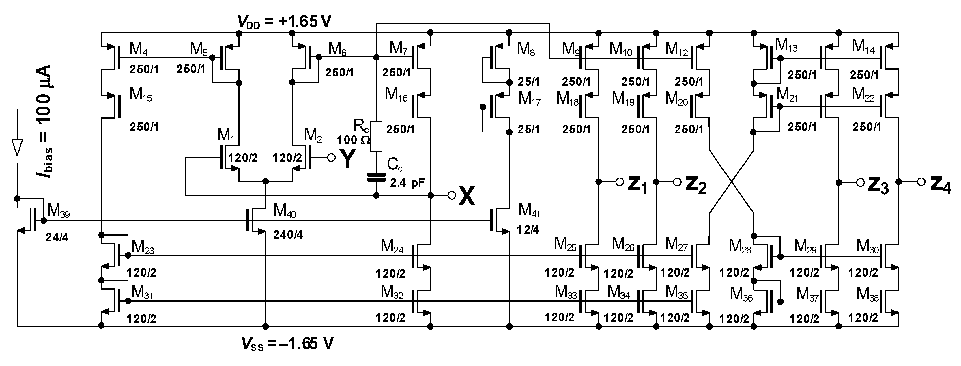
2. Active Devices—Integrated Modular Cells
3. Proposed Designs
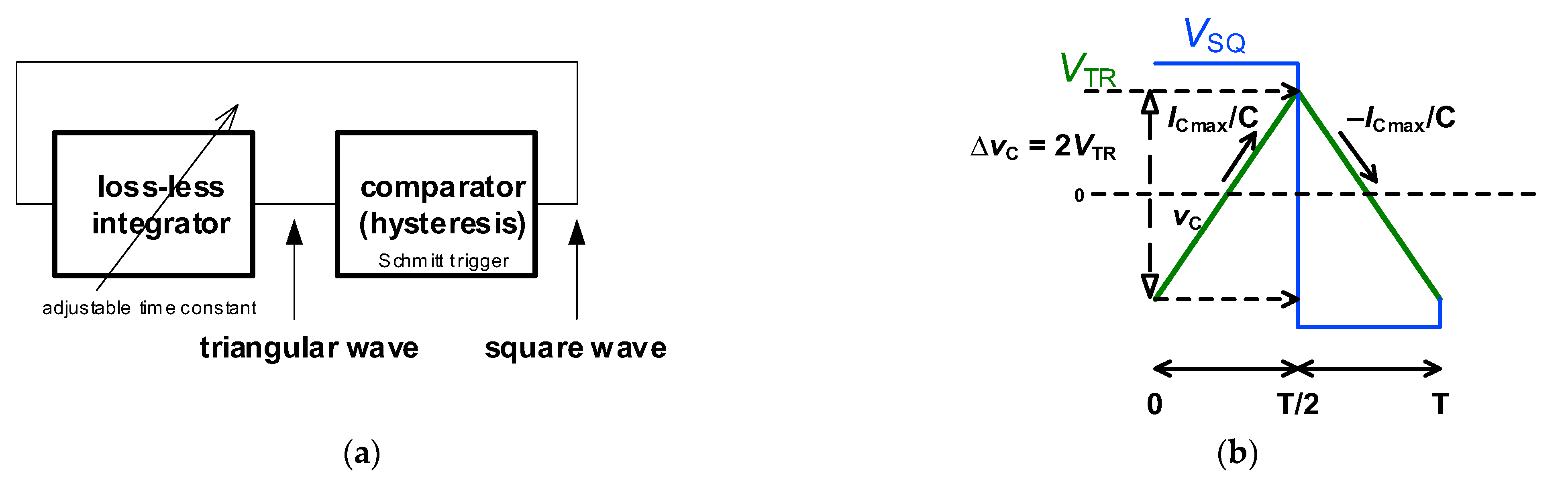
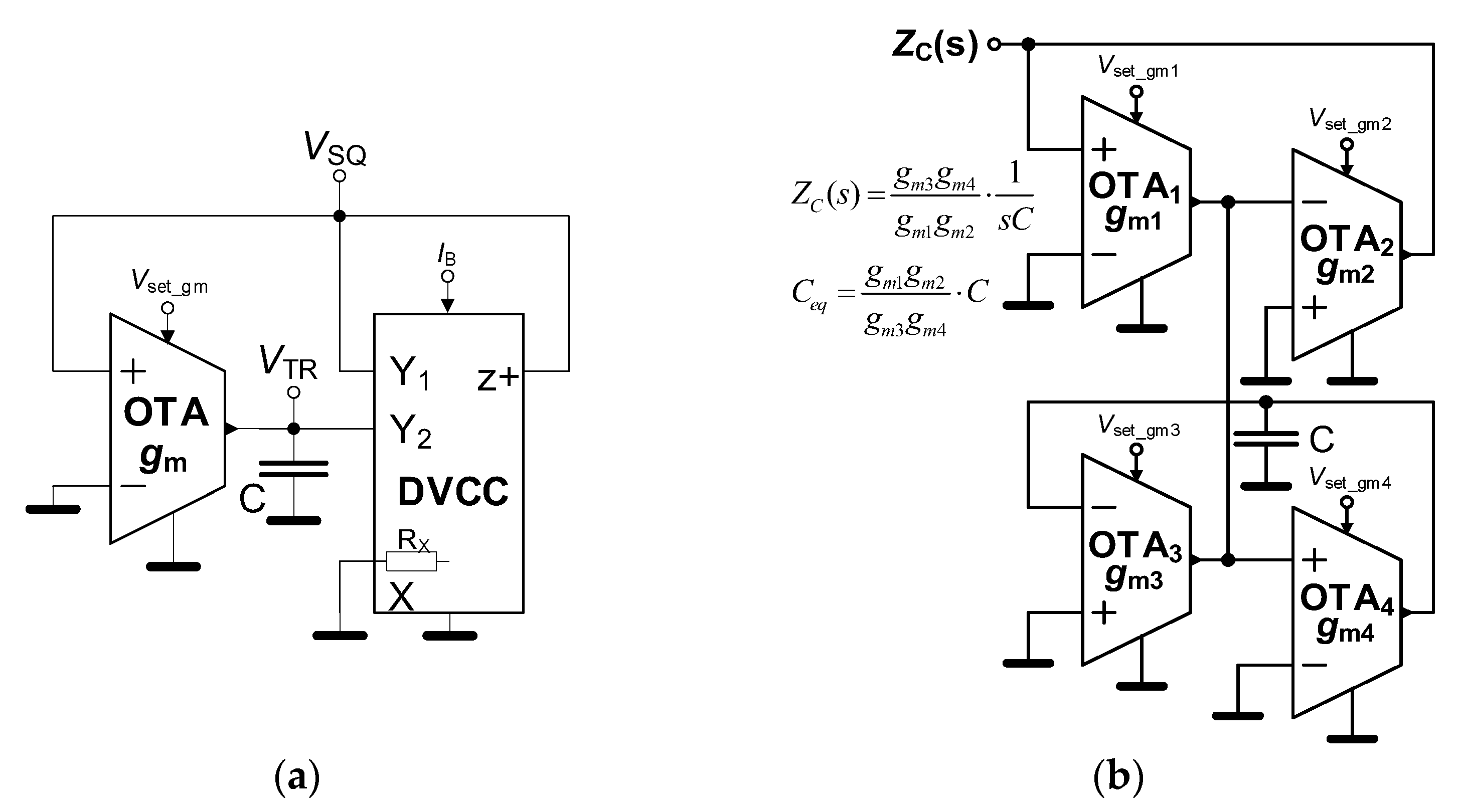
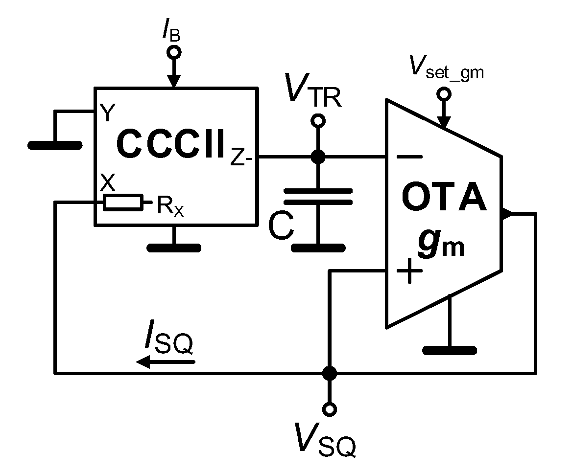
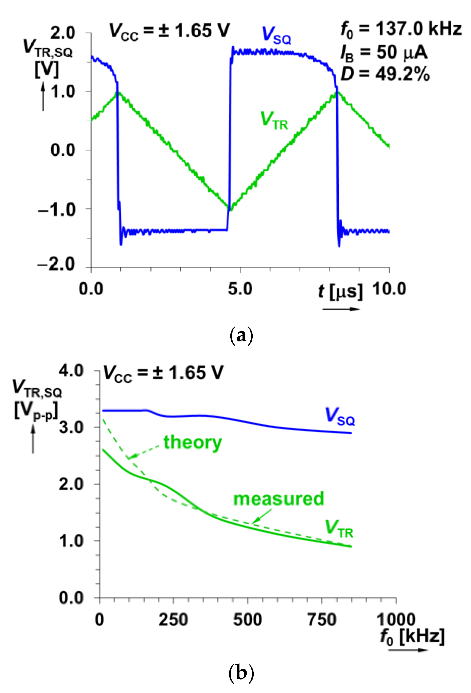
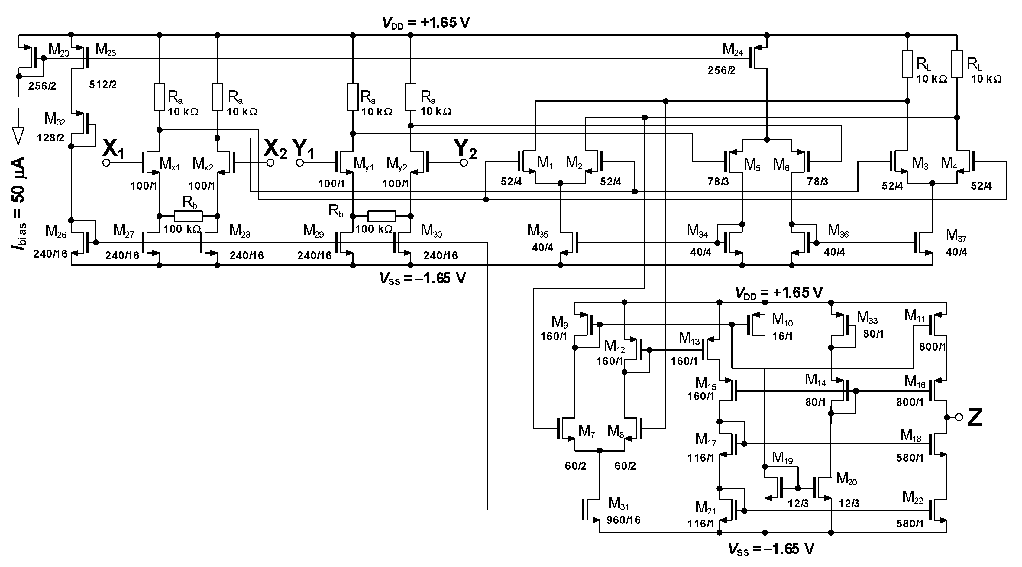
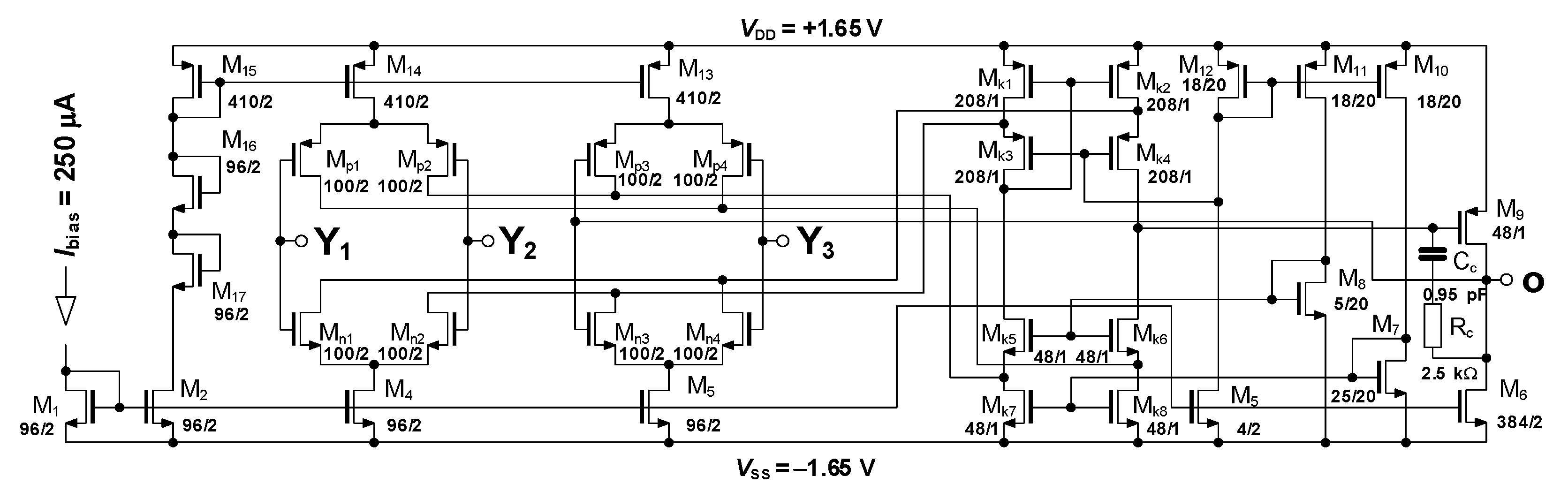
3.1. Resistor-Less Generator Using Voltage Tunable OTA-Based Integrator and Differential Voltage Current Conveyor in Schmitt Trigger
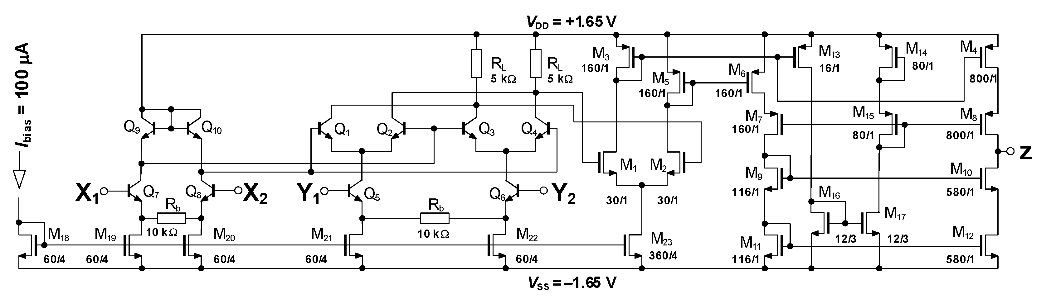
3.2. Resistor-Less Generator Using Current Controlled Current Conveyor of Second Generation-Based Integrator and OTA-Based Schmitt Trigger
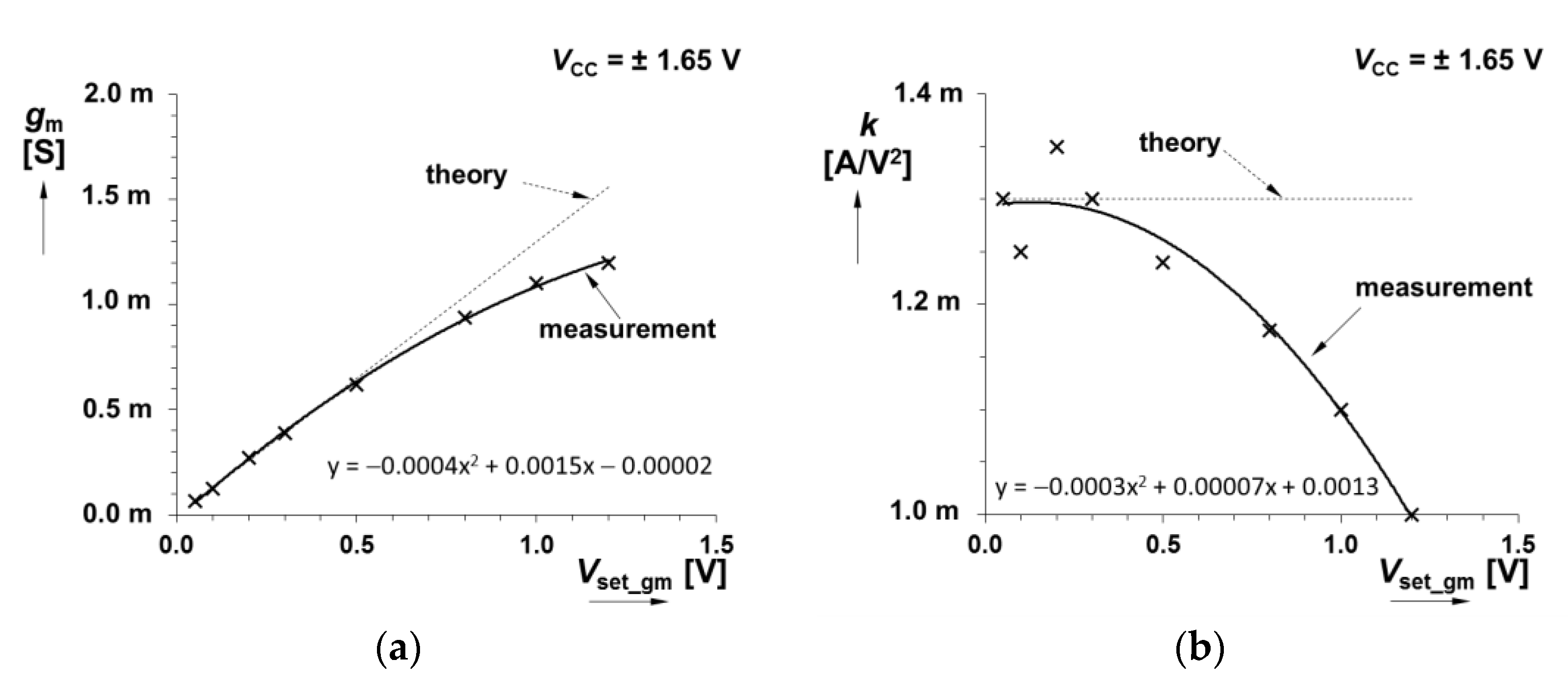
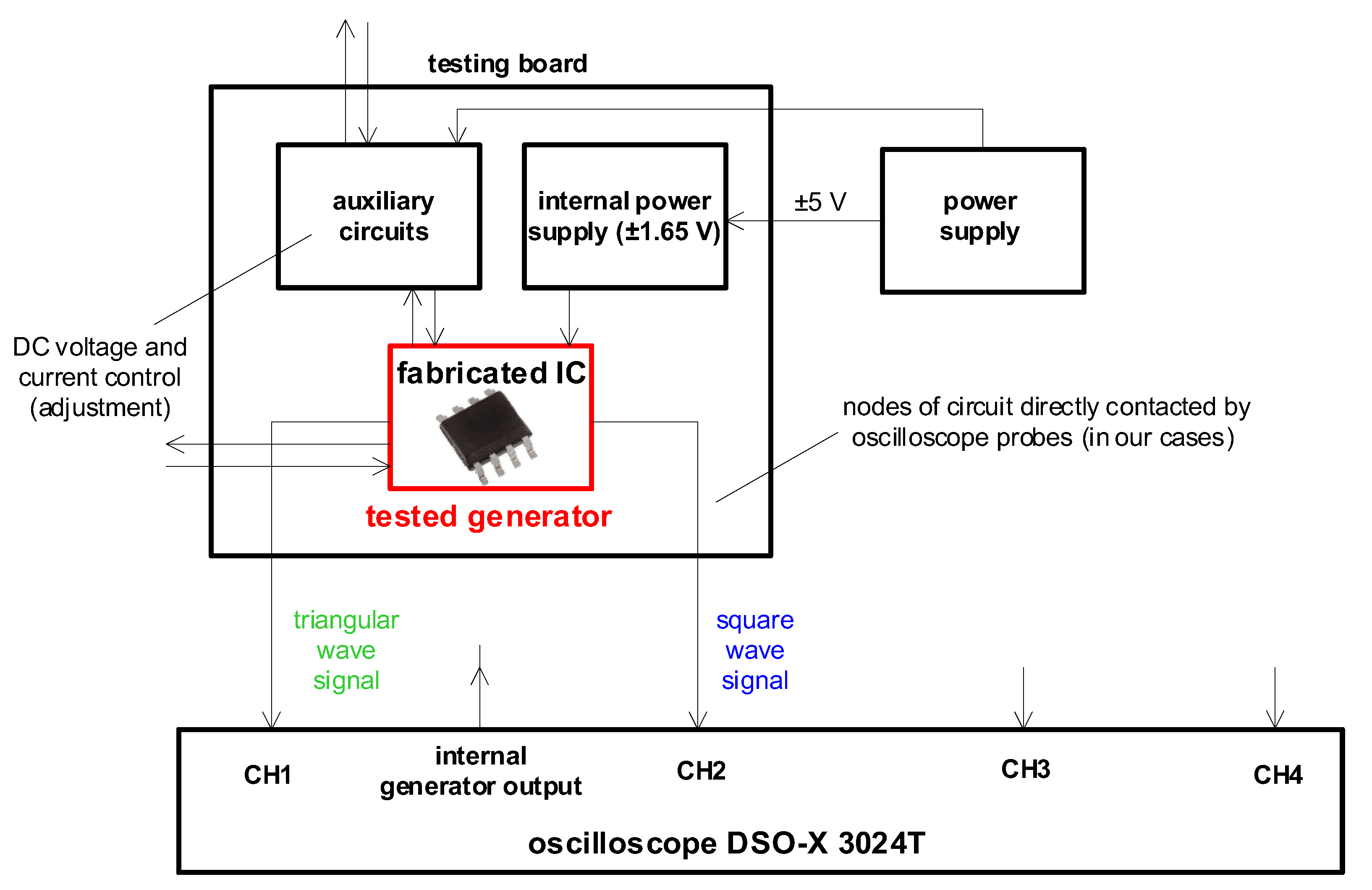
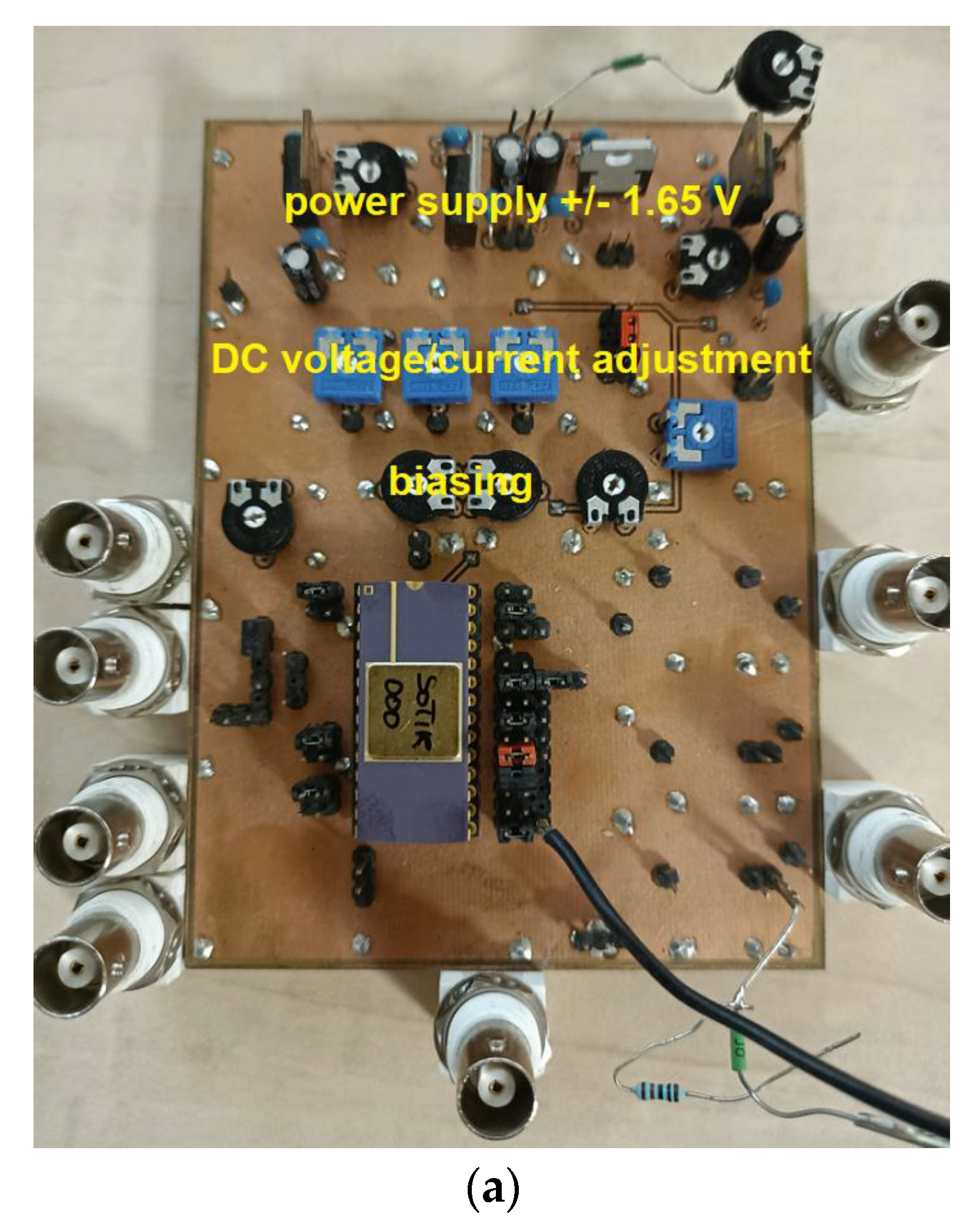
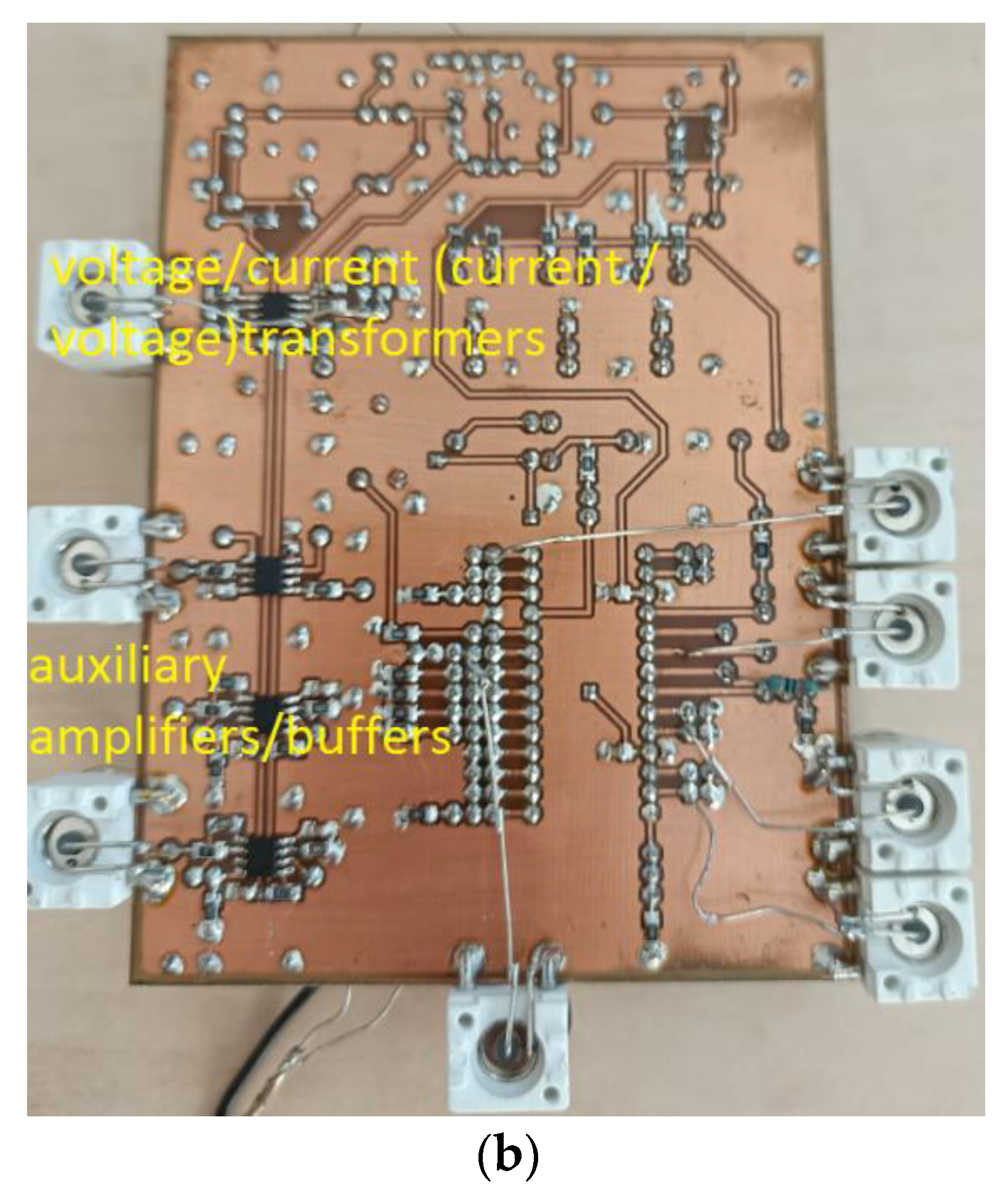
4. Comparison of Both Solutions
5. Conclusions
Author Contributions
Funding
Data Availability Statement
Conflicts of Interest
Appendix A


Appendix B


References
- Senani, R.; Bhaskar, D.R.; Singh, V.K.; Sharma, R.K. Sinusoidal Oscillators and Waveform Generators Using Modern Electronic Circuit Building Blocks; Springer International Publishing AG: Cham, Switzerland; Berlin, Germany, 2016; pp. 1–622. ISBN 978-3-319-23712-1. [Google Scholar] [CrossRef]
- Biolek, D.; Senani, R.; Biolkova, V.; Kolka, Z. Active elements for analog signal processing: Classification, Review and New Proposals. Radioengineering 2008, 17, 15–32. [Google Scholar]
- Senani, R.; Bhaskar, D.R.; Singh, A.K. Current Conveyors: Variants, Applications and Hardware Implementations; Springer International Publishing: Cham, Switzerland; Berlin, Germany, 2015; pp. 1–560. ISBN 978-3-319-08683-5. [Google Scholar] [CrossRef]
- Chung, W.S.; Kim, H.; Cha, H.-W.; Kim, H.-J. Triangular/square-wave generator with independently controllable frequency and amplitude. IEEE Trans. Instrum. Meas. 2005, 54, 105–109. [Google Scholar] [CrossRef]
- Siripruchyanun, M.; Wardkein, P. A full independently adjustable, integrable simple current controlled oscillator and derivative PWM signal generator. IEICE Trans. Fundam. Electron. Commun. Comput. Sci. 2003, 86, 3119–3126. [Google Scholar]
- Kumbun, J.; Siripruchyanun, M. MO-CTTA-based electronically controlled current-mode square/triangular wave generator. In Proceedings of the 1st International Conference on Technical Education (ICTE2009), Bangkok, Thailand, 21–22 January 2010; pp. 158–162. [Google Scholar]
- Silapan, P.; Siripruchyanun, M. Fully and electronically controllable current-mode Schmitt triggers employing only single MO-CCCDTA and their applications. Analog. Integr. Circuits Signal Process. 2011, 68, 111–128. [Google Scholar] [CrossRef]
- Srisakul, T.; Silapan, P.; Siripruchyanun, M. An electronically controlled current-mode triangular/square wave generator employing MO-CCCCTAs. In Proceedings of the 8th International Conference on Electrical Engineering/Electronics, Computer, Telecommunications, and Information Technology, Khon Kaen, Thailand, 17–19 May 2011; pp. 82–85. [Google Scholar]
- Janecek, M.; Kubanek, D.; Vrba, K. Voltage-Controlled Square/Triangular Wave Generator with Current Conveyors and Switching Diodes. Int. J. Adv. Telecommun. Electrotech. Signals Syst. 2012, 1, 76–79. [Google Scholar]
- Sotner, R.; Jerabek, J.; Herencsar, N. Voltage Differencing Buffered/Inverted Amplifiers and Their Applications for Signal Generation. Radioengineering 2013, 22, 490–504. [Google Scholar]
- Sotner, R.; Jerabek, J.; Herencsar, N.; Dostal, T.; Vrba, K. Design of Z-copy controlled-gain voltage differencing current conveyor based adjustable functional generator. Microelectron. J. 2015, 46, 143–152. [Google Scholar] [CrossRef]
- Jerabek, J.; Sotner, R.; Dostal, T.; Vrba, K. Simple Resistor-less Generator Utilizing Z-copy Controlled Gain Voltage Differencing Current Conveyor for PWM Generation. Elektron. Elektrotechnika 2015, 21, 28–34. [Google Scholar]
- Sotner, R.; Petrzela, J.; Jerabek, J.; Domansky, O.; Langhammer, L. Special Electronically Reconfigurable Lossy/Lossless Integrator in Application of Functional Generator. In Proceedings of the 27th International Conference Radioelektronika, Brno, Czech Republic, 19–20 April 2017; pp. 1–5. [Google Scholar]
- Sotner, R.; Jerabek, J.; Herencsar, N.; Prokop, R.; Vrba, K.; Petrzela, J.; Dostal, T. Simply Adjustable Triangular and Square Wave Generator Employing Controlled Gain Current and Differential Voltage Amplifier. In Proceedings of the 23th International Conference Radioelektronika, Pardubice, Czech Republic, 16–17 April 2013; pp. 109–114. [Google Scholar]
- Sotner, R.; Jerabek, J.; Herencsar, N.; Lahiri, A.; Petrzela, J.; Vrba, K. Practical Aspects of Operation of Simple Triangular and Square Wave Generator Employing Diamond Transistor and Controllable Amplifiers. In Proceedings of the 36th International Conference on Telecommunications and Signal Processing (TSP2013), Rome, Italy, 2–4 July 2013; pp. 431–435. [Google Scholar]
- Sotner, R.; Jerabek, J.; Herencsar, N. Study of impact of voltage gain of comparator on performance of newly designed functional generator. Opt. Int. J. Light Electron Opt. 2018, 172, 203–219. [Google Scholar] [CrossRef]
- Chaturvedi, B.; Kumar, A. A novel linear square/triangular wave generator with tunable duty cycle. AEU Int. J. Electron. Commun. 2018, 84, 206–209. [Google Scholar] [CrossRef]
- Kumar, A.; Chaturvedi, B. Single Active Element-Based Tunable Square/Triangular Wave Generator with Grounded Passive Components. Circuits Syst. Signal Process. 2017, 36, 3875–3900. [Google Scholar] [CrossRef]
- Siripruchyanun, M.; Payakkakul, K.; Pipatthitikorn, P.; Satthaphol, P. A Current-mode Square/Triangular ware Generator based on Multiple-output VDTAs. Procedia Comput. Sci. 2016, 86, 152–155. [Google Scholar] [CrossRef][Green Version]
- Chaturvedi, B.; Kumar, A. Fully Electronically Tunable and Easily Cascadable Square/Triangular Wave Generator with Duty Cycle Adjustment. J. Circuits Syst. Comput. 2019, 28, 1950105. [Google Scholar] [CrossRef]
- Kumar, A.; Chaturvedi, B.; Maheshwari, S. A fully electronically controllable Schmitt trigger and duty cycle-modulated waveform generator. Int. J. Circuit Theory Appl. 2017, 45, 2157–2180. [Google Scholar] [CrossRef]
- Sacu, I.E. An Electronically Adjustable Waveform Generator. J. Circuits Syst. Comput. 2020, 29, 2050191. [Google Scholar] [CrossRef]
- Thanyaratsakul, N.; Tanthong, A.; Tritummanurak, T.; Keaw-on, R.; Paponpen, K.; Silapan, P.; Jaikla, W. Single LT1228 Based Electronically Controllable Sawtooth Generator. In Proceedings of the 9th International Electrical Engineering Congress (iEECON), Pattaya, Thailand, 10–12 March 2021; pp. 349–352. [Google Scholar]
- Siripruchyanun, M.; Hirunporm, J. A fully/electronically controllable voltage-mode Schmitt trigger based on only single VDGA and its applications. AEU Int. J. Electron. Commun. 2021, 131, 153602. [Google Scholar] [CrossRef]
- Kumari, S.; Visweswaran, G.S.; Kumari, L. Design and Analysis of Voltage Control Function Generator Using Highly Linear CCII. In Proceedings of the 17th India Council International Conference (INDICON), New Delhi, India, 10–13 December 2020; pp. 1–6. [Google Scholar]
- Chaturvedi, B.; Kumar, A. CMOS MO-CFDITA Based Fully Electronically Controlled Square/Triangular Wave Generator with Adjustable Duty Cycle. IET Circuits Devices Syst. 2018, 12, 817–826. [Google Scholar] [CrossRef]
- Prokop, R.; Musil, V. Modular approach to design of modern circuit blocks for current signal processing and new device CCTA. In Proceedings of the 7th International Conference on Signal and Image Processing, Honolulu, HI, USA, 15–17 August 2005; pp. 494–499. [Google Scholar]
- Prokop, R.; Musil, V. New modular current devices for true current mode signal processing. Electronics 2007, 16, 36–42. [Google Scholar]
- Sotner, R.; Jerabek, J.; Polak, L.; Prokop, R.; Kledrowetz, V. Integrated Building Cells for a Simple Modular Design of Electronic Circuits with Reduced External Complexity: Performance, Active Element Assembly, and an Application Example. Electronics 2019, 8, 568. [Google Scholar] [CrossRef]
- Geiger, R.L.; Sanchez-Sinencio, E. Active filter design using operational transconductance amplifiers: A tutorial. IEEE Circuits Devices Mag. 1985, 1, 20–32. [Google Scholar] [CrossRef]
- Al-Absi, M.A.; Al-Khulaifi, A.A. A New Floating and Tunable Capacitance Multiplier with Large Multiplication Factor. IEEE Access 2019, 7, 120076–120081. [Google Scholar] [CrossRef]
- Sotner, R.; Jerabek, J.; Petrzela, J.; Domansky, O.; Jaikla, W.; Dostal, T. Exponentially tunable voltage controlled quadrature oscillator. In Proceedings of the 40th International Conference on Telecommunications and Signal Processing (TSP), Barcelona, Spain, 5–7 July 2017; pp. 302–306. [Google Scholar]
- Sotner, R.; Jerabek, J.; Herencsar, N.; Petrzela, J. Methods for Extended Tunability in Quadrature Oscillators Based on Enhanced Electronic Control of Time Constants. IEEE Trans. Instrum. Meas. 2018, 67, 1495–1505. [Google Scholar] [CrossRef]
- Jogad, S.; Loan, S.A.; Afzal, N.; Alharbi, A.G. CNTFET based class AB current conveyor II: Design, analysis and waveform generator applications. Int. J. Numer. Modelling Electron. Netw. Devices Fields 2020, 34, e2783. [Google Scholar] [CrossRef]
- Sotner, R.; Jerabek, J.; Polak, L.; Petrzela, J.; Jaikla, W.; Tuntrakool, S. Illuminance Sensing in Agriculture Applications Based on Infra-Red Short-Range Compact Transmitter Using 0.35 um CMOS Active Device. IEEE Access 2020, 8, 18149–18161. [Google Scholar] [CrossRef]
- Sotner, R.; Jerabek, J.; Polak, L.; Prokop, R.; Kledrowetz, V.; Theumer, R.; Langhammer, L. Special analog multipliers in voltage-controlled oscillator and phase-locked loop-based FM demodulator for measurement and processing of sensed low-frequency signals. Measurement 2022, 201, 111734. [Google Scholar] [CrossRef]


| Reference | Number. of Passive Elements (in Lab. Experiments) | Number of Active Elements | Number of IC Packages | Compact IC Device Including All Active Elements | Driving Force | Driving Force Range | Frequency Range (If More Than One, the Widest Reported) | FOM Ratio (f0max: f0min)/(Vset_gmmax: Vset_gmmin) | Type of Active Element(s) | Classification of Active Element(s) Used in Verification | Power Consumption [mW] |
|---|---|---|---|---|---|---|---|---|---|---|---|
| [4] | 3 | 3 | 3 | No | I | 5 µA→5 mA | 1 kHz→900 kHz | 0.90 | OTA | standard | N/A |
| [5] | 3 | 3 | N/A | No | I | 0.1 µA→10 mA | 0.1 kHz→3 MHz | 0.30 | OTA | standard | N/A |
| [6] | 1 | 2 | N/A | No | I | 1 µA→100 µA | 2 kHz→150 kHz | 0.75 | MO-CTTA | hypothetical | N/A |
| [7] | 1 | 2 | N/A | No | I | 1 µA→100 µA | 3 kHz→200 kHz | 0.67 | MO-CCCDTA | hypothetical | N/A |
| [8] | 1 | 2 | N/A | No | I | 1 µA→100 µA | 3 kHz→200 kHz | 0.67 | MO-CCCCTA | hypothetical | 1.6 |
| [9] | 8 | 2 | 1 | Yes | V | 0.05 V→0.7 V | 200 kHz→1.6 MHz | 0.57 | UCC + CCII | fabricated | N/A |
| [10] | 3 | 2 | N/A | No | I | 5 µA→100 µA | 211 kHz→2.83 MHz | 0.67 | VDBA | hypothetical | N/A |
| [11] | 3 | 1 | 5 | No | I | 93 µA→37 µA | 1 MHz→4.39 MHz | 1.75 | ZC-CG-VDCC | hypothetical | 6.3 |
| [12] | 1 | 1 | 8 | No | V | 0.04 V→0.63 V | 11 kHz→110 kHz | 0.63 | ZC-CG-VDCC | hypothetical | N/A |
| [13] | 4 | 3 | 3 | No | V | 0.1 V→3 V * | 2.55 kHz→25 kHz | 0.33 | ECCII + VGA + OPAMP | standard | N/A |
| [14] | 2 | 1 | 2 | No | V | 0.1 V→3.0 V | 0.56 MHz→11.39 MHz | 0.68 | CG-CDVA | hypothetical | N/A |
| [15] | 2 | 3 | 3 | No | V | 0.73 V→1.2 V | 0.5 MHz→2.01 MHz | 1.68 | DT + VGA | standard | N/A |
| [16] | 2 | 2 | 2 | No | V | 0.1 V→1.5 V | 1.16 MHz→6.7 MHz | 0.39 | ECCII + VGA | standard | N/A |
| [17] | 2 (4) | 1 | 7 | No | I | 0.5 mA→2 mA | 5 kHz→25 kHz | 1.25 | MO-DXCCTA | hypothetical | N/A |
| [18] | 2 (4) | 1 | 6 | No | I | 0.1 mA→0.2 mA | 8 kHz→16.5 kHz | 1.03 | MO-DVCCTA | hypothetical | 226 |
| [19] | 3 | 2 | N/A | No | I | 1 µA→1 mA | 3 kHz→2 MHz | 0.67 | MO-VDTA | hypothetical | 14.3 |
| [20] | 2 (4) | 1 | 8 | No | I | 1 µA→55 µA | 1.69 MHz→3.88 MHz | 0.04 | MO-DXCCTA | hypothetical | 1 |
| [21] | 1(2) | 1 | 5 | No | I | 10 µA→80 µA | 13 MHz→75 MHz | 0.72 | MO-CIDITA | hypothetical | ** |
| [22] | 1 (5) | 1 | 3 | No | I | 10 µA→80 µA | 8 kHz→58 kHz | 0.91 | MO-CCCCTA | hypothetical | 0.27 |
| [23] | 3 | 2 | 2 | No | I | 10 µA→100 µA | 20 kHz→120 kHz | 0.60 | OTA + CFOA + inverter | standard | N/A |
| [24] | 4 | 2 | 4 | No | I | 100 µA→500 µA | 4 kHz→9 kHz | 0.45 | VDGA | hypothetical | 1.39 |
| [25] | 4 | 6 | N/A | No | V | 0.58 V→1.2 V | 27 MHz→48 MHz | 0.86 | CCCII | standard | 11.32 |
| [26] | 2 | 1 | 3 | No | I | 50 µA→150 µA | 1.27 kHz→3.65 kHz | 0.97 | MO-CFDITA | hypothetical | 1.25 |
| Proposed | |||||||||||
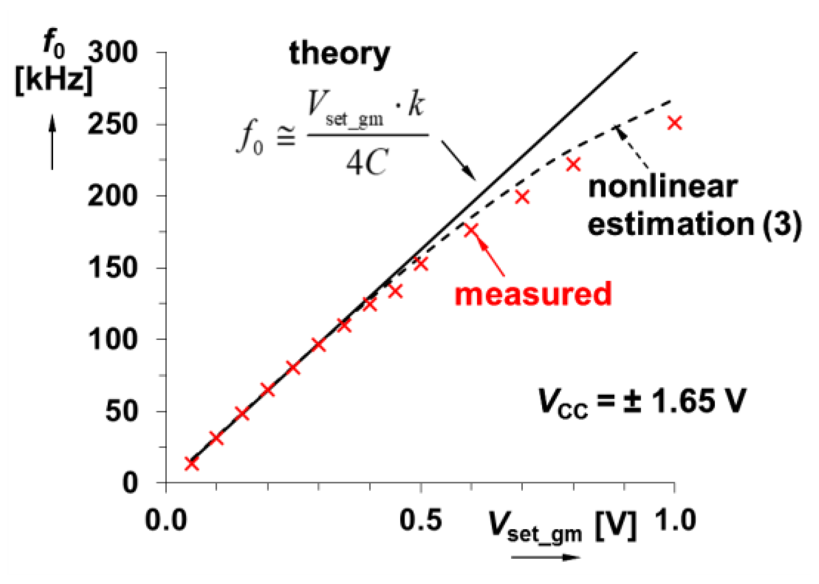
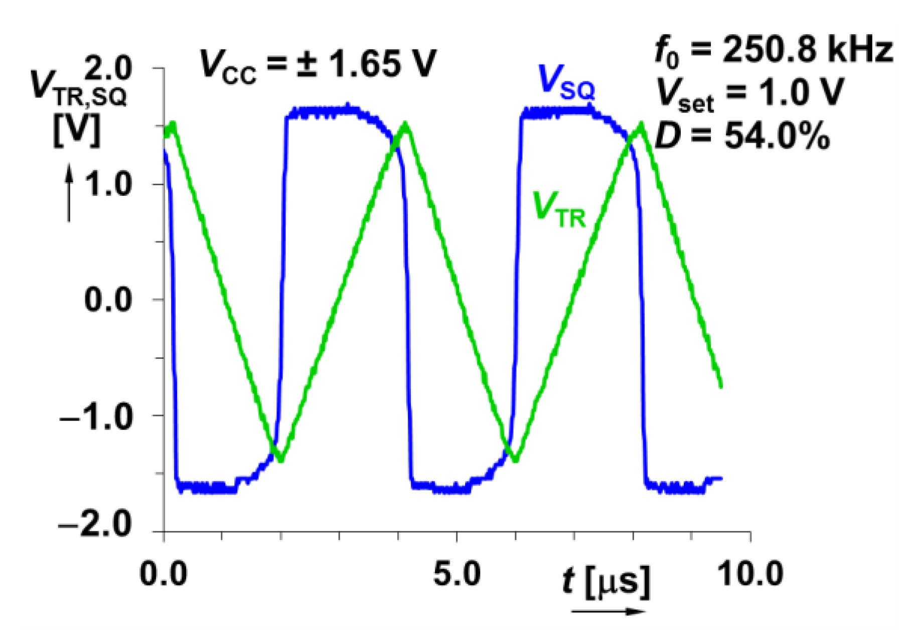
| Section 3.1 | 1 | 2 (3) # | 1 | Yes | V | 0.05 V→1.0 V | 13 kHz→251 kHz | 0.96 | OTA + DVCC (OTA + VDDB + CCCII) | fabricated | 43 |
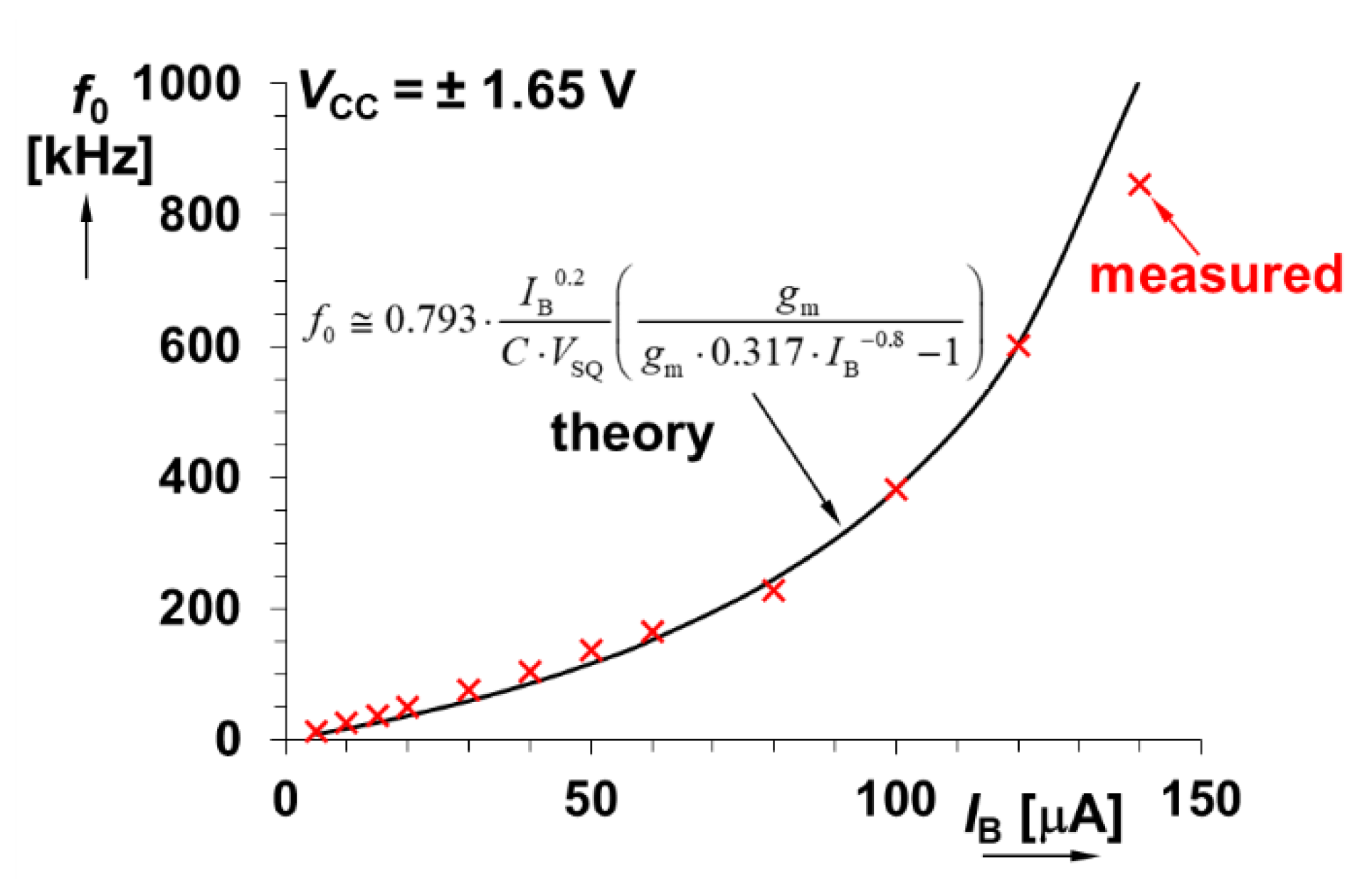
| Section 3.2 | 1 | 2 | 1 | Yes | I | 5 µA→140 µA | 12 kHz→847 kHz | 2.52 | CCCII + OTA | fabricated | 41 |
| Figure 3 | Figure 7 | |
|---|---|---|
| Parameter for f0 tuning | gm (Vset_gm) | RX (IB) |
| DC control range (full tested) | 0.05 V→1.0 V | 5 µA→140 µA |
| Range of f0 tuning (full tested) | 13 kHz→251 kHz | 12 kHz→847 kHz |
| Ratio (f0max: f0min)/(Vset/IB max: Vset/IB min) | 0.96 | 2.52 |
| Number of passive elements | 1 | 1 |
| Number of cells of IC used | 3 | 2 |
| Suitable for high-speed applications | No | Yes |
| Power consumption | 43 mW | 41 mW |
| Note | high-impedance output node of comparator | product gm∙RX of the comparator influences triangular level when tuned |
Publisher’s Note: MDPI stays neutral with regard to jurisdictional claims in published maps and institutional affiliations. |
© 2022 by the authors. Licensee MDPI, Basel, Switzerland. This article is an open access article distributed under the terms and conditions of the Creative Commons Attribution (CC BY) license (https://creativecommons.org/licenses/by/4.0/).
Share and Cite
Sotner, R.; Jerabek, J. Mathematical Expressions Useful for Tunable Properties of Simple Square Wave Generators. Mathematics 2022, 10, 4528. https://doi.org/10.3390/math10234528
Sotner R, Jerabek J. Mathematical Expressions Useful for Tunable Properties of Simple Square Wave Generators. Mathematics. 2022; 10(23):4528. https://doi.org/10.3390/math10234528
Chicago/Turabian StyleSotner, Roman, and Jan Jerabek. 2022. "Mathematical Expressions Useful for Tunable Properties of Simple Square Wave Generators" Mathematics 10, no. 23: 4528. https://doi.org/10.3390/math10234528
APA StyleSotner, R., & Jerabek, J. (2022). Mathematical Expressions Useful for Tunable Properties of Simple Square Wave Generators. Mathematics, 10(23), 4528. https://doi.org/10.3390/math10234528