Article

Generation of a Synthetic Database for the Optical Response of One-Dimensional Photonic Crystals Using Genetic Algorithms

by
Cesar Isaza
,
Ivan Alonso Lujan-Cabrera
,
Ely Karina Anaya Rivera
,
Jose Amilcar Rizzo Sierra
,
Jonny Paul Zavala De Paz
and
Cristian Felipe Ramirez-Gutierrez
*,†
Cuerpo Académico de Tecnologías de la Información y Comunicación Aplicada, Universidad Politécnica de Querétaro, El Marqués, Querétaro 76230, Mexico
*
Author to whom correspondence should be addressed.
These authors contributed equally to this work.
Mathematics 2022, 10(23), 4484; https://doi.org/10.3390/math10234484
Submission received: 28 October 2022 / Revised: 19 November 2022 / Accepted: 23 November 2022 / Published: 28 November 2022
(This article belongs to the Special Issue Evolutionary Computation 2022)

Abstract

:
This work proposes an optimization tool based on genetic algorithms for the inverse design of photonic crystals. Based on target reflectance, the algorithm generates a population of chromosomes where the genes represent the thickness of a layer of a photonic crystal. Each layer is independent of another. Therefore, the sequence obtained is a disordered configuration. In the genetic algorithm, two dielectric materials are first selected to generate the population. Throughout the simulation, the chromosomes are evaluated, crossed over, and mutated to find the best-fitted one based on an error function. The target reflectance was a perfect mirror in the visible region. As a result, it was found that obtaining photonic crystal configurations with a specific stop band with disordered arrangements is possible. The genetic information of the best-fitted individuals (layer sequence, optical response, and error) is stored in an h5 format. This method of generating artificial one-dimensional photonic crystal data can be used to train a neural network for solving the problem of the inverse design of any crystal with a specific optical response.
MSC:
78-10; 78A10; 90-08; 90B40

1. Introduction

Photonic crystals (PC) have received much attention as a novel material that uses its optical capabilities to manipulate light on a wavelength scale [1,2]. A photonic crystal should be understood as a material having a periodic variation in its refractive index or dielectric function in space [3] which produces bandgaps in a specific wavelength range where light cannot propagate (zero transmittance) [4]. The refractive index contrasts and the lattice parameters determine the bandwidth and spectral position of the photonic bandgap [5].
Wave optics and solid-state physics collide to form the concept of photonic crystals. As an extension of multidimensional periodicity, the dielectric constant can be tailormade periodically in one, two, or three dimensions. In particular, one-dimensional photonic crystals can be made of layers of dielectric materials such as semiconductors [6,7], polymers [8,9], composites [10], or porous materials [11,12,13] arranged in alternating layers of high and low reflective index materials [14].
This kind of structure has many potential applications in subjects related to optical science and technology. For instance, optic modulators, sensing [15], microcavity-based or distributed feedback lasers [16], and solar cells [17].
Recent advances in photonic crystals have been discussed in several fields ranging from bandgap/defect engineering to optical system designing. However, the major problem in obtaining a specific optical response lies in the analytical methods. This is because there is a complex relationship between material optical properties and PC spatial distribution, especially for absorbent and dispersive materials. Moreover, this leads to a master equation [18], which describes the electromagnetic field distribution with a non-hermitian operator. Then, one way to approach the design of specific optical responses is the usual trial and error framework or human intuition design. However, it is ineffective and has little experimental reality. In addition, the optical response is not unique. Different geometries and material mixtures can produce a similar optical response involving a degenerated problem as far as light propagation is concerned. Despite this, and far from being a disadvantage, it is necessary to explore unordered [19] configurations such as modulated [12,20], incommensurately or random photonic crystals [21] that can generate devices with geometries that can be easily manufactured.
Machine learning (ML) strategies are becoming common ways to rapidly conduct a thorough design space search. Deep neural networks and other supervised learning techniques have attracted much interest lately. According to the universal approximation theorem, complex mapping functions may be represented in a neural network design. To construct forward and inverse models for predicting the attributes of PC devices, the network of several layers of neurons makes it possible to learn complex mathematical functions [22]. Therefore, ML algorithms can be used to calculate the geometrical parameters and material mixtures required, which is a promising approach for inverse design [23,24,25]. The inverse design problem or the direct finding of the correct structure for the required optical response is usually guided by optimization algorithms [26] such as genetic algorithms [11,27,28] or particle swarm algorithms [29]. However, because of their random-search character, such stochastic algorithms are insufficient for complicated design. Other works report the uses of artificial neural networks (NN) to predict the optical response [30] (forward-modeling) and inverse-design [23,31,32] of a device as an alternative to replacing expensive computational electromagnetic simulations. Inverse design using neural networks requires many training scenarios before it can execute the target function. Then, training the neural network is the key to the inverse design. However, there are few available experimental data, or these are repeated (same configurations). As an alternative, GA can be used to generate artificial datasets for successfully NN training in different fields [33,34]. For this reason, this work proposes introducing a genetic algorithm to generate an artificial database of one-dimensional photonic crystals and take advantage of an artificial neural network to create different structures of photonic crystals and compare them. During the optimization procedure, the genetic algorithm creates a large amount of data (reflectance and transmittance) that can be used for NN training.

2. Physical Model of Wave Propagation in Thin Films

The transfer matrix method (TMM) was used to study the optical properties of one-dimensional photonic crystals (1DPCs) [35]. This method allows the construction of a multilayer structure, where each layer is nonmagnetic and has a complex refractive index ( η = n + i k ), here, n is the refractive index and k is the extinction coefficient. In addition, a system air-PC-air was considered. The transfer matrix M relates the electric and magnetic fields at two arbitrary points as follows [36]:
E 0 H 0 = M E 1 H 1 .
The optical admittance Y j is defined as
Y j = H j E j ,
and depends on the polarization. For s-polarization, admittance is
Y j s = H j E j = η c o s θ j ,
whereas for p-polarization
Y j p = H j E j = η c o s θ j .
Two equations are obtained by applying boundary conditions for the j-th interface,
E j R + E j L = E j R + E j L ,
Y j 1 E j R Y j 1 E j L = Y j E j R Y j E j L .
From Equations (5) and (6), the Fresnel coefficients for right propagation are
r j R = E j L E j R = Y j 1 Y j Y j 1 + Y j ,
t j R = E j R E j R = 2 Y j 1 Y j 1 + Y j .
Equations (5) and (6) can be represented in a matrix with elements expressed in terms of the Fresnel coefficients. Thus, the admittance matrix is defined as follows:
W j 1 , j = c j 1 , j t j + 1 , j 1 r j R r j R 1 ,
where
c j 1 , j = c o s θ j 1 c o s θ j for p-polarization , 1 for s-polarization .
The transfer matrix can be written as:
M = W j 1 , j U j W j , j + 1 U j + 1 . . . .
where j represents the layer, W j 1 , j and U j represent the admittance and phase matrix, respectively. The admittance matrix describes the interface between two layers (Equation (9)), and the phase matrix represents each layer and is defined as follows:
U j = e i β d 0 0 e i β d ,
where
β = 2 π η λ c o s θ ,
here, λ is the wavelength, η the complex refractive index and θ the angle of incidence.
Since the transfer matrix is a 2 × 2 matrix, it can be expressed by its elements.
M = M 11 M 12 M 21 M 22 .
The Fresnel coefficients r and t, and the reflectance ( R ) and transmittance ( T ) spectra for the structure, are given as a function of the elements in Equation (14).
r = M 21 M 11 , R = r r * ,
t = 1 M 11 , T = t t * .
Equations (15) and (16) are valid for S and P polarization using the adequate polarization coefficient (Equation (10)). In the case of unpolarized light:
R = 1 2 R s + R p , T = 1 2 T s + T p ,
where R s , T s , R p and T p are the reflectance and transmittance for S and P polarization, respectively.

3. Genetic Algorithms

The Genetic Algorithm (GA) is stochastic; however, it can estimate the global optimum of a given problem and maintain the best solution for each generation. In addition, the evolution history contains information on the physical model of electromagnetic wave propagation (transfer matrix method) and the optical properties of the pair materials. Then, the GA can be used to obtain a 1DPC with specific reflection spectra. As Figure 1a shows, it is started by elaborating the desired optical response, in this case, the reflectance spectrum that corresponds to a mirror with a reflectance level of 0 R m a x 1 , where R m a x = 0 and R m a x = 1 correspond to an ideal antireflector (black mirror) and ideal mirror, respectively. According to the design requirements, the reflectance level ( R m a x ) , the resonance wavelength ( λ 0 ) , and bandwidth ( Δ λ ) are fixed. Previous experimental [11,37] and computational [12] reports show that dielectric materials are absorbent in the visible range. Therefore, the radiation intensity is attenuated exponentially as a function of the thickness of the films. Then, the simulation can be limited to a finite number of layers. However, 1DPCs are susceptible to producing nearly identical optical responses with different configurations. It means that design space has degenerated (Figure 1b) [31,38]. So, in this case, the simulations were performed with five unit cells corresponding to ten individual layers ( m = 10 ) of intercalated materials. Figure 2 shows an overview of the GA used to generate the sequence of the 1DPC layers to approximate the desired optical response.
Generally, the GA uses the thickness of each layer as a gene that makes up the chromosome. Each chromosome can be expressed as:
T = ( d 1 , d 2 , d 3 , d 4 , d 5 , . . . , d m ) ,
where T is the chromosome, d i is the thickness of the i-th layer, and m is the total number of layers in the 1DPC structure. It means that the chromosome contains the photonic crystal sequence.
Each chromosome has an associated error related to the target reflection spectra. Operators, such as mutation and selection, are used in GA to minimize the error. The error is defined as the following function.
E r r o r = λ = λ m i n λ m a x ( R 0 ( λ ) R ( λ ) ) 2 N ,
where R 0 ( λ ) is the target reflection, and N is the total number of wavelengths in the interval from λ min to λ max . Lastly, R ( λ ) is the reflection spectrum calculated from the sequence in the chromosome.
First, the pair of materials is selected from a database that contains the optical properties (complex refractive index), and the number of layers (m) is fixed (see Figure 2a)). Then, the GA begins by creating a starting population of n p o p members, each with a randomized list of layer thicknesses. The starting population is a parent list and can be expressed as the following set:
P = { T 1 , T 2 , . . . , T n p o p } .
Each parent in P is evaluated according to Equation (19) to determine the best-fitted parents. Then, the population set P is rearranged as a function of each individual error, starting with the best-fitted one as Figure 2b shows. The steady state-based selection method was used to generate 50% of the offspring. Meanwhile, to avoid a local minimum, the other 50% is selected by a random-based method with a uniform probability.
After the evaluation of the population, a crossover process is performed (Figure 2c). There are two sexual crossover methods. The first method generates the offspring through two processes.
  • First of all, the best-fitted individual is crossed with the best-fitted half of the population, generating half of the offspring. The offspring inherits an average value between the genetic information of the two parents (elitist crossover, see Figure 2c).
  • Second, the other half of the population is generated from two individuals randomly selected from the population. A random crossover point in the chromosome is generated. Before that point, the new individual inherits the genetic information of one of the parents, and after the crossover point, the genetic information of the second parent (one-point crossover, see Figure 2c).
The second method is the one-point crossover. The only difference is that the whole population is generated instead. Both methods have a 0.5 probability of occurrence.
A mutation process is required to avoid local minimums (Figure 2d). In GA, the factor for the mutation process is typically lower than 2% of the genes [39]. However, experimental results showed that if an enormous value is used by the design of a photonic crystal, the optimal function is reached, and the objective function factor increases. Therefore, approximately 20% of the offspring is mutated. There are two equally possible ways in which the individual can mutate. The first is a Gaussian mutation where all the genes are randomly selected from a normal distribution curve centered in the value of the original gene ( μ ) and with a specific standard deviation ( σ ). The second method completely changes the chromosome of the individual and replaces it with a new one. Suppose there is no improvement from one generation to the next one. In that case, the percentage of the mutated population and the standard deviation ( σ ) of the normal distribution curve are increased to obtain more genetic variability in the offspring.
After completing the previous steps, the GA will search for the best-fitted chromosome of the generation, and a new population will be generated. This process is repeated until the GA reaches a minimum error or a certain number of generations.

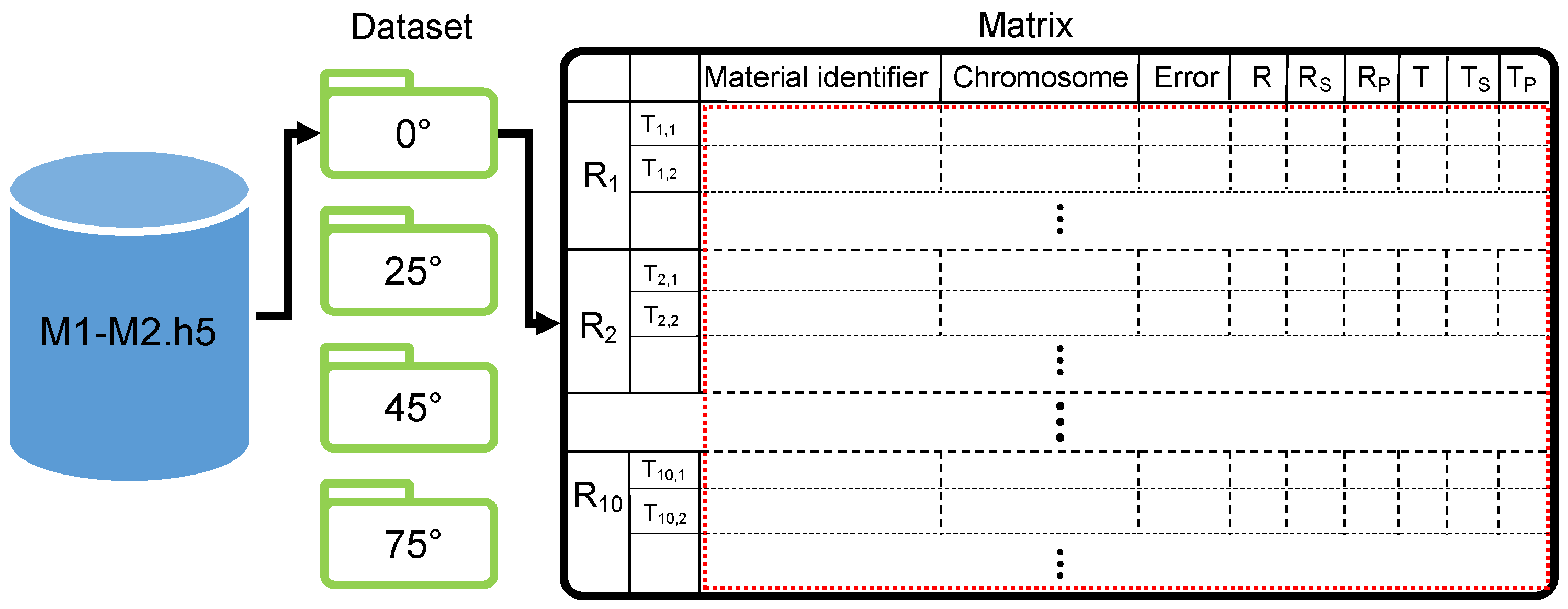
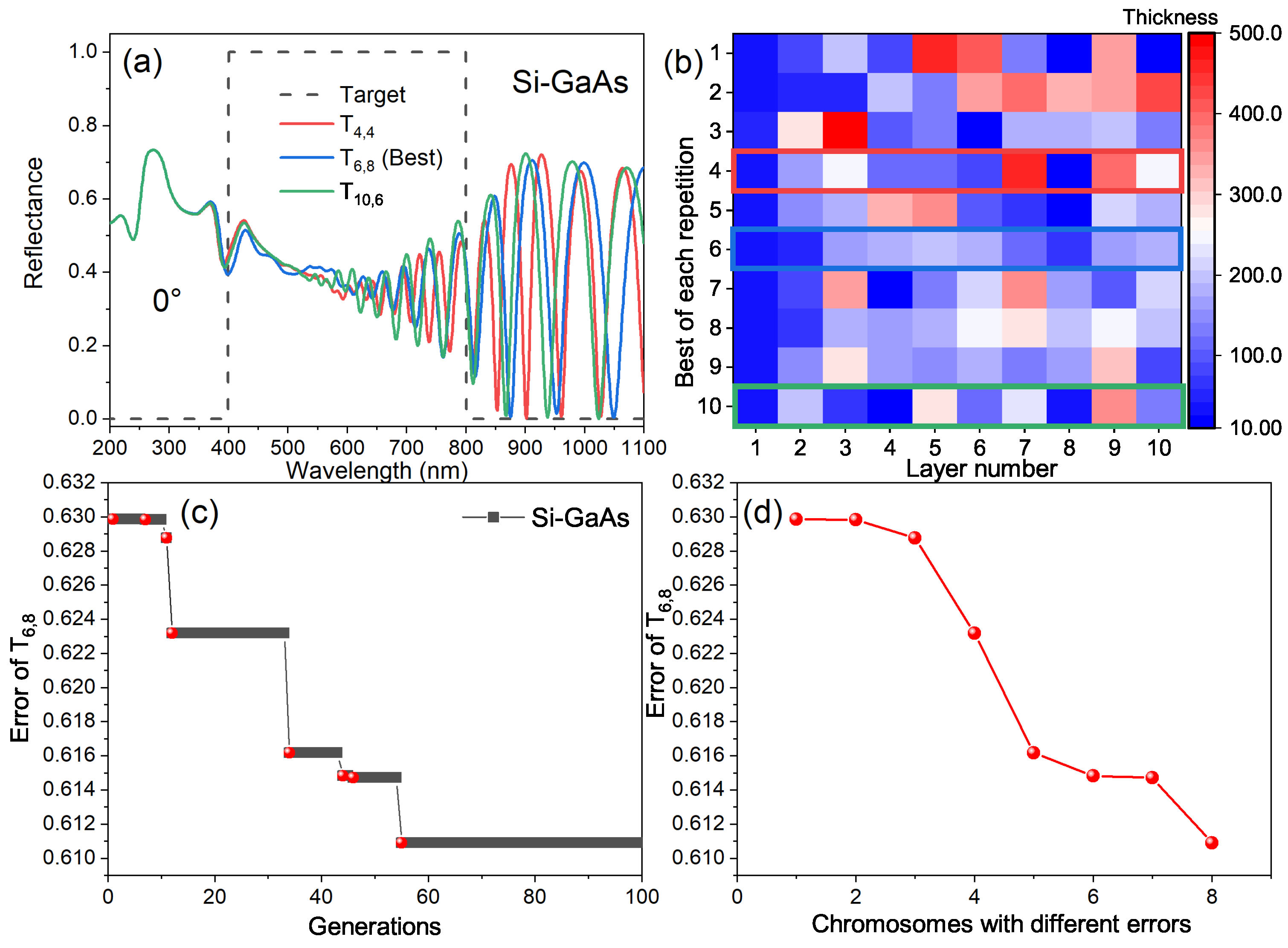
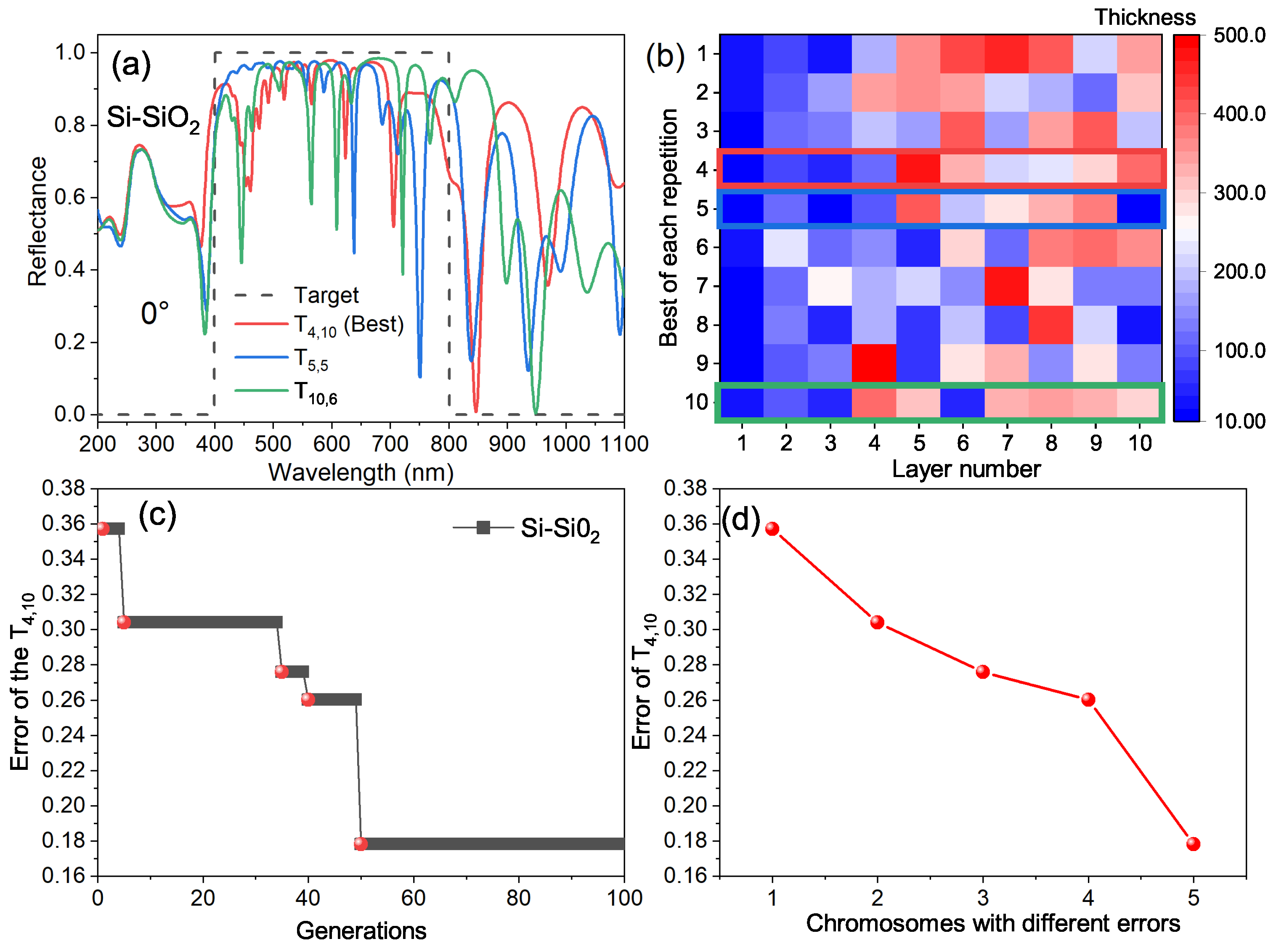
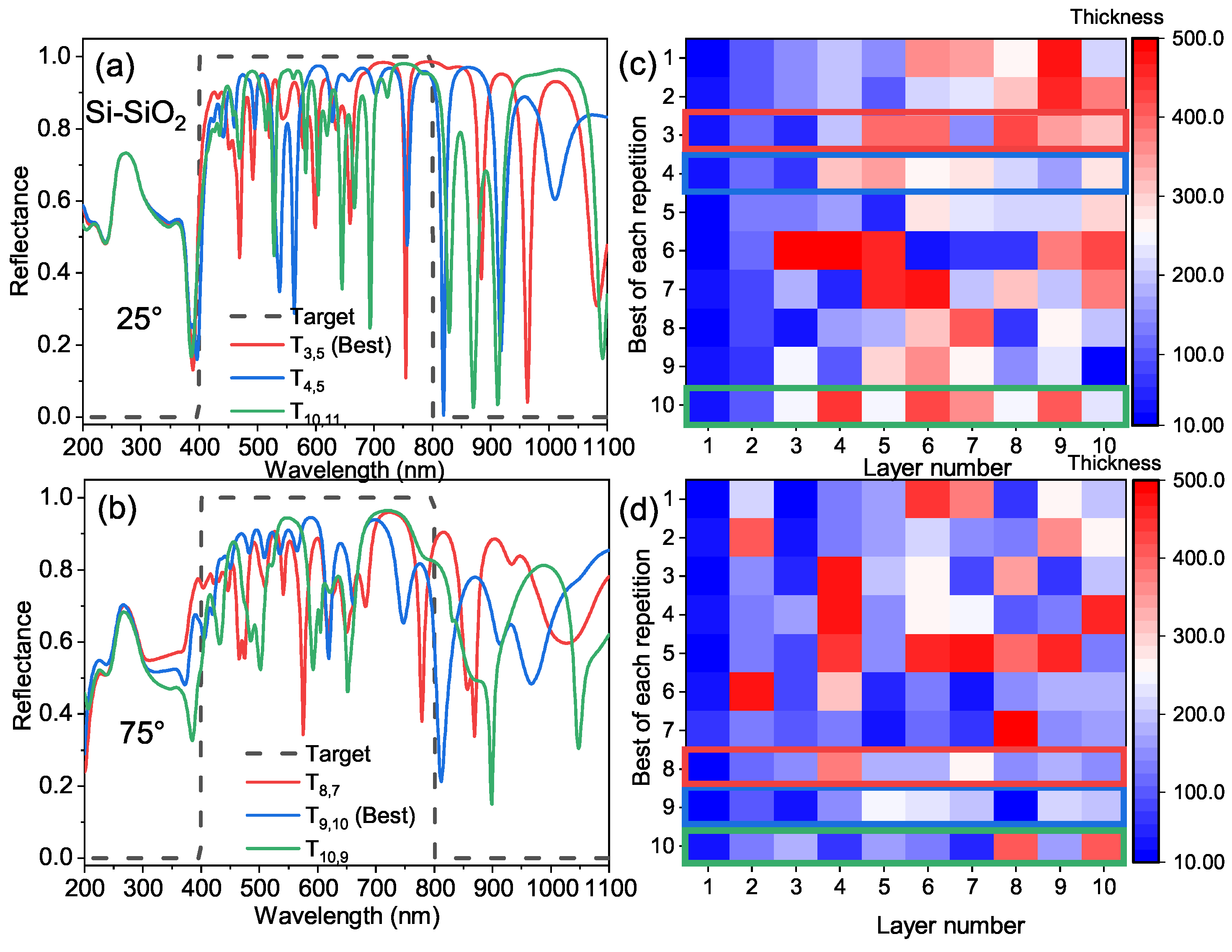
4. Results and Discussion

Generalizing conclusions from an initial training dataset is the foundation of machine learning. This suggests that bias in the training and evaluation data may have a non-negligible impact on network training optimization and assessed performance statistics.
A proper density of training data must be generated for a good quality database representing manufacturable optical devices with practical reality. Then, the user of the GA routine can set the value for the following critical parameters: the material pairs, the total number of layers (must be even), target spectra, spectral optimization interval, output spectra range (restringed for the available experimental data known for the materials optical constants) and spectral resolution (a minimum of 1 nm). Finally, this program can be adapted to generate a particular database for specific purposes in the above-mentioned parameters.
For the generation of the database, the GA described in the previous section was coded and tested in Python (see Appendix A for pseudo code) to resemble a target reflectance which in this case is the optical response of a perfect reflector in the visible region. This means a mirror whose reflectance is 1 in the visible region and 0 otherwise. The optical response of a PC of 10 layers (five periods of two interlarded dielectric materials) was simulated to achieve this. The optical constants were chosen from a set of 19 materials. Only dielectric and nonmagnetic materials (see Table 1) were selected to ensure the boundary conditions of the electromagnetic field on the interface between two materials, as the TMM requires [40].
Table 2 shows critical parameter constraints related to the GA and the PC used in the simulations for each repetition. For the PC, a minimum layer thickness of 10 nm was chosen to guarantee films with the same optical properties as their bulk. Moreover, that restriction allows the PC to be manufactured by experimental techniques such as chemical deposition, electrochemical etching, and photolithography, among others. The maximum number of layers was constrained to 10 because the contribution of more layers would be negligible due to the non-zero absorption coefficient of the materials used. Four angles were simulated (0 , 25 , 45 and 75 ) to obtain information about the optical response considering the light polarization. Finally, the target reflectance sets the optimization range, bandwidth, and maximum reflectance.
On the other hand, the parameters used for the GA were chosen to ensure algorithm convergence and minimize the computation time.
Given that the optical response depends on the geometric arrangement of the two selected materials, all the possible configurations (324 different PC with different materials) were simulated.
The general performance of the GA for the database generation is as follows: from the list of dielectric materials (Table 1), two are selected to calculate the optical response of a ten layers PC. The GA was run for 100 generations for four angles, 0 , 25 , 45 , and 75 , respectively. The best-fitted and non-repeated individual of each generation is saved in the database. Only the individuals with genetic variability are held. Then, the total number of individuals saved is not initially defined because it depends on the genetic evolution in each repetition. This process is repeated ten times to obtain a proper density of training data.
The data is stored in an h5 file, whose name is composed of the two materials used. In the h5 file, four datasets were created, containing all the selected individuals for each angle, respectively. This is represented in Figure 3. The data is stored in a matrix form. Each row contains all the information of the individual T n , m , which is the m-th individual stored from the n-th repetition. The first columns of each row represent the information on which two materials are being simulated in the PC. Each material has assigned a column number. A number 1 is printed in the corresponding column number of the material if that material is been used in the simulation, and 0 otherwise. After this, the error of the individual is stored. The following columns held information related to the optical response (R, R s , R p , T, T s , and T p ).
Some representative results are shown in Figure 4, Figure 5, Figure 6 and Figure 7. In particular, two cases are exposed in these figures. The first is a case where the materials are not suitable for the fabrication of a perfect reflector in the visible range (Figure 4 and Figure 5) because GaAs is highly absorbent and dispersive in the target spectral region. The second is where the two materials generate an optical response that resembles the perfect reflector (Figure 6 and Figure 7). These materials were selected because Si and SiO 2 are low absorbent and dispersive in the target spectral region.
Furthermore, in Figure 4a and Figure 6a, the optical response of three PC, with an incident angle of 0 , are compared with a perfect reflector (target). The plotted spectra represent the three best-fitted chromosomes among the ten repetitions. In Figure 4b and Figure 6b, each row represents the sequence of 10 layers of each PC. The color indicates the thickness of the layers. Chromosomes plotted in Figure 4a and Figure 6a are highlighted with their respective color.
Figure 4c and Figure 6c display the error of the best chromosome (found in the ten repetitions) as a function of the generations. As can be seen, the error remains constant at about the 50th generation, which evidences a convergence of the GA. The generation where a chromosome with different genetic information was found is highlighted with a red dot. In Figure 4d and Figure 6d the error of these chromosomes is plotted, and it is worth noticing that only these were stored in the h5 file to avoid saving repeated data.
Figure 5a and Figure 7a show the optical response of three PC simulated with an incident angle of 25 and Figure 5c and Figure 7c show the complete set of the best chromosome of each repetition. As mentioned above, the three selected chromosomes are highlighted in their respective colors. Finally, Figure 5b and Figure 7b display the optical response of three PC simulated with an incident angle of 75 and Figure 5d and Figure 7d show the complete set of the best chromosome of each repetition. These simulations give information about the behavior of the optical response of the PC as a function of the polarization of the light. This allows the design, simulation, and possible fabrication of a wide variety of optical devices with specific characteristics at specific incident angles.
For case one, it is noticeable that the resemblance between the three PC and the target is not good, having an associated error of around 0.612 for the best-fitted chromosome. For case two, the optical response of the simulated PC adjusts better to the target reflectance. However, the error also exposes this because it is lower than 0.18. It is evident that the solutions found by the GA are disordered as shown in Figure 4, Figure 5, Figure 6 and Figure 7. Nevertheless, all the previously mentioned results present a pattern in common. The first layer has a thickness of about 30 nm. This is because the materials used are highly absorbent near the UV region. Thus, the shorter wavelengths are mainly absorbed in the first layer, which means that the layer must be thin (smaller than the wavelength), so the radiation can reach the second layer, and interference conditions can occur.
Therefore, the best two materials to obtain a PC with a specific optical response with a disorder configuration critically depend on the fabrication technique, the target reflectance, the optimization region, and the refractive indexes of the materials in that region.

5. Conclusions

An optimization tool based on genetic algorithms for the inverse design of photonic crystals is proposed. The algorithm proposes a chromosome where each gene is the thickness of a series of intercalated films that evolves until approaching a target optical response. However, this evolutionary strategy that subjects individuals to various evolutionary actions generates many outputs that preserve the PC layer sequence, the materials, and the theoretical model of electromagnetic wave propagation in thin films (TMM). Consequently, these data can be discriminated against and saved because they help train a neural network later. The algorithm corresponds to a strategy to generate artificial training data for neural networks. A selection of dielectric materials was made to generate this database. Next, the optical constants of these materials were obtained from the refractiveindex.INFO database and homogenized using data interpolation strategies. Finally, the general routine selects a material and combines it with the other materials, generating all possible permutations, and the generated data is saved in an h5 file data structure. This algorithm mainly shows that it is possible to obtain photonic crystal configurations with a specific stop band with disordered configurations. These unordered configurations can be advantageous for manufacturing because they result in thicknesses that are easy to handle and produce with the conventional techniques currently in use. In addition, the algorithm can be adapted to other mathematical models, for example, for metallic or magnetic systems. Moreover, it can restrict the values of the thicknesses and number of layers so that it approximates the practical reality of the manufacturable sequences. On the other hand, this approach has certain limitations such as the long computation time to obtain a complete database, the transfer matrix method is only for dielectric materials and the optical constants of these materials, determined by experimental methods, must be available.
Finally, this method of generating artificial one-dimensional photonic crystal data may be optimized by using neural networks for the inverse design of any crystal with a specific optical response, such as perfect mirrors or black mirrors.

Author Contributions

Conceptualization, C.I., I.A.L.-C. and C.F.R.-G.; Data curation, C.I., I.A.L.-C. and C.F.R.-G.; Formal analysis, I.A.L.-C., J.P.Z.D.P. and C.F.R.-G.; Funding acquisition, C.I. and E.K.A.R.; Investigation, I.A.L.-C. and C.F.R.-G.; Methodology, C.I., I.A.L.-C., E.K.A.R., J.A.R.S. and C.F.R.-G.; Resources, C.I., E.K.A.R. and J.P.Z.D.P.; Software, C.I., I.A.L.-C. and E.K.A.R.; Supervision, C.I., I.A.L.-C. and C.F.R.-G.; Validation, I.A.L.-C., J.A.R.S. and C.F.R.-G.; Visualization, I.A.L.-C. and C.F.R.-G.; Writing—original draft, C.I., I.A.L.-C. and C.F.R.-G.; Writing—review & editing, C.I., I.A.L.-C., J.A.R.S., J.P.Z.D.P. and C.F.R.-G. All authors have read and agreed to the published version of the manuscript.

Funding

This research received no external funding.

Institutional Review Board Statement

Not applicable.

Data Availability Statement

The data presented in this study are available on request from the corresponding author.

Acknowledgments

The authors are eternally grateful for the scholarships provided by SNI program from CONACYT-Mexico.

Conflicts of Interest

The author declares no conflict of interest or competing interest.

Abbreviations

The following abbreviations are used in this manuscript:
PCPhotonic crystal
MLMachine Learning
NNNeural Network
TMMTransfer Matrix Method
1DPCsOne-dimensional photonic crystals
GAGenetic Algorithm

Appendix A

Pseudo code of the GA for the database generation
  • Libraries import
  • #Initialization of variables
  • N_population 30 #Number of individuals
  • Generations 100 #Maximum number of generations
  • Repetitions 10 #Number of repetitions
  • Sigma 1 #Standard deviation for Gaussian mutation
  • Ter_cond 0.05 #Termination condition
  • N_layers 10 #Number of layers
  • Import optical constants from local directory
  • Define the target reflectance
  • Generate a random initial population
  • for all materials − 1 do
  • for all materials − 1 do
  •   Set h5 file
  •   for all angles do
  •    for i ≤ generations do
  •     Calculate Reflectance of the population (Transfer matrix method)
  •     Calculate The fitness of each individual (Error)
  •     Calculate Sort the population by fitness
  •     Reproduce the population (Average and one-point crossover)
  •     Mutation of the individuals (Gaussian and random mutation)
  •     Selection of the individuals (Steady state and Random Methods)
  •     Determine the best individual
  •     if error_best < Ter_cond then
  •      Stop
  •     end if
  •     Plot the reflectance
  •     Set the new population
  •     Save data in h5 file (Materials used, chromosome, error, reflectance)
  •    end for
  •   end for
  •   Close h5 file
  • end for
  • end for

References

  1. Butt, M.; Khonina, S.; Kazanskiy, N. Recent advances in photonic crystal optical devices: A review. Opt. Laser Technol. 2021, 142, 107265. [Google Scholar] [CrossRef]
  2. Saeidi, F.S.; Moradi, M. A new route to designing a one-dimensional multiperiodic photonic crystal with adjustable photonic band gap and enhanced electric field localization. Opt. Commun. 2021, 493, 126999. [Google Scholar] [CrossRef]
  3. Vigneron, J.P.; Simonis, P. Natural photonic crystals. Phys. B Condens. Matter 2012, 407, 4032–4036. [Google Scholar] [CrossRef]
  4. Kavokin, A.V.; Baumberg, J.J.; Malpuech, G.; Laussy, F.P. Microcavities; Oxford University Press: Oxford, UK, 2017; Volume 21, pp. 52–59. [Google Scholar]
  5. Chen, C.W.; Hou, C.T.; Li, C.C.; Jau, H.C.; Wang, C.T.; Hong, C.L.; Guo, D.Y.; Wang, C.Y.; Chiang, S.P.; Bunning, T.J.; et al. Large three-dimensional photonic crystals based on monocrystalline liquid crystal blue phases. Nat. Commun. 2017, 8, 727. [Google Scholar] [CrossRef] [PubMed] [Green Version]
  6. Iwamoto, S.; Ota, Y.; Arakawa, Y. Recent progress in topological waveguides and nanocavities in a semiconductor photonic crystal platform [Invited]. Opt. Mater. Express 2021, 319–337. [Google Scholar] [CrossRef]
  7. Li, Y.; Xiang, Y.; Wen, S.; Yong, J.; Fan, D. Tunable terahertz-mirror and multi-channel terahertz-filter based on one-dimensional photonic crystals containing semiconductors. J. Appl. Phys. 2011, 110, 073111. [Google Scholar] [CrossRef]
  8. Edrington, A.C.; Urbas, A.M.; DeRege, P.; Chen, C.X.; Swager, T.M.; Hadjichristidis, N.; Xenidou, M.; Fetters, L.J.; Joannopoulos, J.D.; Fink, Y.; et al. Polymer-Based Photonic Crystals. Adv. Mater. 2001, 13, 421–425. [Google Scholar] [CrossRef]
  9. Robertson, M.; Sanford, A.; Qiang, Z. Easy to Pattern, Chemically Resistant One-Dimensional Polymer Photonic Crystals. ACS Appl. Polym. Mater. 2021, 3, 2626–2634. [Google Scholar] [CrossRef]
  10. Zhang, L.; Xu, Q.; Sun, C.; Peng, Q.; Lan, T.; Dong, M.; Xiao, Y.; Zhang, J. Synthesis and properties of iridescent Ni–Co composite photonic crystal films by pulse anodization. Ceram. Int. 2021, 47, 16276–16281. [Google Scholar] [CrossRef]
  11. Ramirez-Gutierrez, C.F.; Martinez-Hernandez, H.D.; Lujan-Cabrera, I.A.; Rodriguez-García, M.E. Design, fabrication, and optical characterization of one-dimensional photonic crystals based on porous silicon assisted by in-situ photoacoustics. Sci. Rep. 2019, 9, 14732. [Google Scholar] [CrossRef]
  12. Ortiz-Vazquez, E.; Lujan-Cabrera, I.; Isaza, C.; Rizzo-Sierra, J.; Ramirez-Gutierrez, C. Design of broadband modulated one-dimensional photonic crystals based on porous silicon using evolutionary search. Optik 2022, 260, 169002. [Google Scholar] [CrossRef]
  13. Calvo, M.E.; Colodrero, S.; Hidalgo, N.; Lozano, G.; López-López, C.; Sánchez-Sobrado, O.; Míguez, H. Porous one dimensional photonic crystals: Novel multifunctional materials for environmental and energy applications. Energy Environ. Sci. 2011, 4, 4800–4812. [Google Scholar] [CrossRef]
  14. Yablonovitch, E. Inhibited Spontaneous Emission in Solid-State Physics and Electronics. Phys. Rev. Lett. 1987, 58, 2059–2062. [Google Scholar] [CrossRef] [PubMed] [Green Version]
  15. Normani, S.; Dalla Vedova, N.; Lanzani, G.; Scotognella, F.; Paternò, G.M. Design of 1D photonic crystals for colorimetric and ratiometric refractive index sensing. Opt. Mater. X 2020, 8, 100058. [Google Scholar] [CrossRef]
  16. Komikado, T.; Yoshida, S.; Umegaki, S. Surface-emitting distributed-feedback dye laser of a polymeric multilayer fabricated by spin coating. Appl. Phys. Lett. 2006, 89, 061123. [Google Scholar] [CrossRef]
  17. Mihi, A.; Míguez, H. Origin of Light-Harvesting Enhancement in Colloidal-Photonic-Crystal-Based Dye-Sensitized Solar Cells. J. Phys. Chem. B 2005, 109, 15968–15976. [Google Scholar] [CrossRef] [PubMed] [Green Version]
  18. Joannopoulos, J.D.; Johnson, S.G.; Winn, J.N.; Meade, R.D. Photonic Crystals: Molding the Flow of Light, 2nd ed.; Princeton University Press: Princeton, NJ, USA, 2008. [Google Scholar]
  19. Wiersma, D.S. Disordered photonics. Nat. Photonics 2013, 7, 188–196. [Google Scholar] [CrossRef]
  20. Tanaka, Y.; Nishigo, A.; Kitamura, K.; Gelleta, J.; Noda, S. Modulated photonic-crystal surface-emitting laser with elliptical lattice points for two-dimensional coupling enhancement. AIP Adv. 2019, 9, 115204. [Google Scholar] [CrossRef]
  21. Bellingeri, M.; Chiasera, A.; Kriegel, I.; Scotognella, F. Optical properties of periodic, quasi-periodic, and disordered one-dimensional photonic structures. Opt. Mater. 2017, 72, 403–421. [Google Scholar] [CrossRef] [Green Version]
  22. Singh, R.; Agarwal, A.; Anthony, B.W. Mapping the design space of photonic topological states via deep learning. Opt. Express 2020, 28, 27893–27902. [Google Scholar] [CrossRef] [PubMed]
  23. Zhan, T.; Liu, Q.S.; Sun, Y.J.; Qiu, L.; Wen, T.; Zhang, R. A general machine learning-based approach for inverse design of one-dimensional photonic crystals toward targeted visible light reflection spectrum. Opt. Commun. 2022, 510, 127920. [Google Scholar] [CrossRef]
  24. Yao, K.; Unni, R.; Zheng, Y. Intelligent nanophotonics: Merging photonics and artificial intelligence at the nanoscale. Nanophotonics 2019, 8, 339–366. [Google Scholar] [CrossRef] [PubMed]
  25. Hegde, R.S. Deep learning: A new tool for photonic nanostructure design. Nanoscale Adv. 2020, 2, 1007–1023. [Google Scholar] [CrossRef]
  26. Ma, W.; Liu, Z.; Kudyshev, Z.A.; Boltasseva, A.; Cai, W.; Liu, Y. Deep learning for the design of photonic structures. Nat. Photonics 2021, 15, 77–90. [Google Scholar] [CrossRef]
  27. Ramirez-Gutierrez, C.; Castaño-Yepes, J.; Rodriguez-Garcia, M. Porosity and roughness determination of porous silicon thin films by genetic algorithms. Optik 2018, 173, 271–278. [Google Scholar] [CrossRef] [Green Version]
  28. Parinam, S.; Kumar, M.; Kumari, N.; Karar, V.; Sharma, A.L. An improved optical parameter optimisation approach using Taguchi and genetic algorithm for high transmission optical filter design. Optik 2019, 182, 382–392. [Google Scholar] [CrossRef]
  29. He, S.; Liu, Q.; Sa, T.; Wang, Z. Design of broadband reflector at the visible wavelengths using particle swarm optimization. AIP Adv. 2019, 9, 075301. [Google Scholar] [CrossRef] [Green Version]
  30. Alagappan, G.; Png, C.E. Prediction of electromagnetic field patterns of optical waveguide using neural network. Neural Comput. Appl. 2021, 33, 2195–2206. [Google Scholar] [CrossRef]
  31. Unni, R.; Yao, K.; Zheng, Y. Deep Convolutional Mixture Density Network for Inverse Design of Layered Photonic Structures. ACS Photonics 2020, 7, 2703–2712. [Google Scholar] [CrossRef]
  32. Liu, D.; Tan, Y.; Khoram, E.; Yu, Z. Training Deep Neural Networks for the Inverse Design of Nanophotonic Structures. ACS Photonics 2018, 5, 1365–1369. [Google Scholar] [CrossRef]
  33. Romanov, O.; Lysenko, O. The evolutionary computation method for the synthesis of networks-on-chip quasi-optimal topologies. In Proceedings of the 2014 IEEE 34th International Scientific Conference on Electronics and Nanotechnology (ELNANO), Kyiv, Ukraine, 15–18 April 2014; pp. 403–407. [Google Scholar] [CrossRef]
  34. Zunin, V.; Romanov, A.; Solovyev, R. Developing Methods for Combinational Circuit Generation. In Proceedings of the 2022 International Russian Automation Conference (RusAutoCon), Sochi, Russia, 4–10 September 2022; pp. 842–846. [Google Scholar] [CrossRef]
  35. Mitsas, C.L.; Siapkas, D.I. Generalized matrix method for analysis of coherent and incoherent reflectance and transmittance of multilayer structures with rough surfaces, interfaces, and finite substrates. Appl. Opt. 1995, 34, 1678–1683. [Google Scholar] [CrossRef] [PubMed]
  36. Missoni, L.L.; Ortiz, G.P.; Martínez Ricci, M.L.; Toranzos, V.J.; Mochán, W.L. Rough 1D photonic crystals: A transfer matrix approach. Opt. Mater. 2020, 109, 110012. [Google Scholar] [CrossRef]
  37. Yue, Y.; Gong, J.P. Tunable one-dimensional photonic crystals from soft materials. J. Photochem. Photobiol. C Photochem. Rev. 2015, 23, 45–67. [Google Scholar] [CrossRef]
  38. Dai, P.; Sun, K.; Yan, X.; Muskens, O.L.; de Groot, C.H.K.; Zhu, X.; Hu, Y.; Duan, H.; Huang, R. Inverse design of structural color: Finding multiple solutions via conditional generative adversarial networks. Nanophotonics 2022, 11, 3057–3069. [Google Scholar] [CrossRef]
  39. Greenwell, R.; Angus, J.; Finck, M. Optimal mutation probability for genetic algorithms. Math. Comput. Model. 1995, 21, 1–11. [Google Scholar] [CrossRef]
  40. Lujan-Cabrera, I.; Ramirez-Gutierrez, C.; Castaño-Yepes, J.; Rodriguez-Garcia, M. Effects of the interface roughness in the optical response of one-dimensional photonic crystals of porous silicon. Phys. B Condens. Matter 2019, 560, 133–139. [Google Scholar] [CrossRef]
  41. Polyanskiy, M.N. Refractive Index Database. Available online: https://refractiveindex.info (accessed on 5 October 2022).
  42. Pastrňák, J.; Roskovcová, L. Refraction Index Measurements on AlN Single Crystals. Phys. Status Solidi B 1966, 14, K5–K8. [Google Scholar] [CrossRef]
  43. Larruquert, J.I.; Pérez-Marín, A.P.; García-Cortés, S.; de Marcos, L.R.; Aznárez, J.A.; Méndez, J.A. Self-consistent optical constants of sputter-deposited B4C thin films. J. Opt. Soc. Am. A 2012, 29, 117–123. [Google Scholar] [CrossRef] [PubMed]
  44. Larruquert, J.I.; de Marcos, L.V.R.; Méndez, J.A.; Martin, P.J.; Bendavid, A. High reflectance ta-C coatings in the extreme ultraviolet. Opt. Express 2013, 21, 27537–27549. [Google Scholar] [CrossRef] [Green Version]
  45. de Marcos, L.V.R.; Larruquert, J.I.; Méndez, J.A.; Aznárez, J.A. Self-consistent optical constants of MgF2, LaF3, and CeF3 films. Opt. Mater. Express 2017, 7, 989–1006. [Google Scholar] [CrossRef] [Green Version]
  46. Aspnes, D.E.; Kelso, S.M.; Logan, R.A.; Bhat, R. Optical properties of AlxGa1-x As. J. Appl. Phys. 1986, 60, 754–767. [Google Scholar] [CrossRef]
  47. Aspnes, D.E.; Studna, A.A. Dielectric functions and optical parameters of Si, Ge, GaP, GaAs, GaSb, InP, InAs, and InSb from 1.5 to 6.0 eV. Phys. Rev. B 1983, 27, 985–1009. [Google Scholar] [CrossRef]
  48. Lajaunie, L.; Boucher, F.; Dessapt, R.; Moreau, P. Strong anisotropic influence of local-field effects on the dielectric response of α-MoO3. Phys. Rev. B 2013, 88, 115141. [Google Scholar] [CrossRef] [Green Version]
  49. Beal, A.R.; Hughes, H.P. Kramers-Kronig analysis of the reflectivity spectra of 2H-MoS2, 2H-MoSe2 and 2H-MoTe2. J. Phys. C Solid State Phys. 1979, 12, 881–890. [Google Scholar] [CrossRef]
  50. Singh, S.; Potopowicz, J.R.; Van Uitert, L.G.; Wemple, S.H. Nonlinear Optical Properties of Hexagonal Silicon Carbide. Appl. Phys. Lett. 1971, 19, 53–56. [Google Scholar] [CrossRef]
  51. Malitson, I.H. Interspecimen Comparison of the Refractive Index of Fused Silica. J. Opt. Soc. Am. 1965, 55, 1205–1209. [Google Scholar] [CrossRef]
  52. Kaiser, W.; Spitzer, W.G.; Kaiser, R.H.; Howarth, L.E. Infrared Properties of CaF2, SrF2, and BaF2. Phys. Rev. 1962, 127, 1950–1954. [Google Scholar] [CrossRef]
  53. Bright, T.J.; Watjen, J.I.; Zhang, Z.M.; Muratore, C.; Voevodin, A.A.; Koukis, D.I.; Tanner, D.B.; Arenas, D.J. Infrared optical properties of amorphous and nanocrystalline Ta2O5 thin films. J. Appl. Phys. 2013, 114, 083515. [Google Scholar] [CrossRef]
  54. Pflüger, J.; Fink, J.; Weber, W.; Bohnen, K.P.; Crecelius, G. Dielectric properties of TiCx, TiNx, VCx, and VNx from 1.5 to 40 eV determined by electron-energy-loss spectroscopy. Phys. Rev. B 1984, 30, 1155–1163. [Google Scholar] [CrossRef]
  55. DeVore, J.R. Refractive Indices of Rutile and Sphalerite. J. Opt. Soc. Am. 1951, 41, 416–419. [Google Scholar] [CrossRef]
  56. Jung, G.H.; Yoo, S.; Park, Q.H. Measuring the optical permittivity of two-dimensional materials without a priori knowledge of electronic transitions. Nanophotonics 2019, 8, 263–270. [Google Scholar] [CrossRef]
Figure 1. (a) Target reflectance spectrum and example of 10-layer designs. (b) Design spaced representation of the inverse design of photonic structures that implies a many-to-one problem. Each point in this hyperspace represents a chromosome containing all the layer thicknesses ( d i ) of the photonic crystal sequence and its corresponding optical response (reflectance and transmittance). The graph shows that multiple designs correspond to identical optical responses (indicated by the dashed lines), exhibiting a high degeneracy.
Mathematics 10 04484 g001
Figure 2. Overview of the GA used to optimize the reflectance spectrum of a one-dimensional photonic crystal. (a) A pair of different dielectric materials and their optical constants are chosen from the local database to generate a set of chromosomes randomly. These individuals will go through (b) selection, (c) crossing-over, and (d) mutation rounds to discover individuals capable of producing a specific optical response.
Mathematics 10 04484 g002
Figure 3. Structure of the h5 file The file contains indicators for the materials used, the thickness values of the photonic crystal series, and reflectance and transmittance for polarized (S and P) and unpolarized light.
Mathematics 10 04484 g003
Figure 4. The optimization results for a Si-GaAs PC: (a) The black dashed lines represent the target reflectance, while the solid colored curves show the characteristic optimized spectra corresponding to the best individuals of each run for 0 of incidence; (b) Solution to the individual chromosome representation; (c) Genetic algorithm convergence process; (d) Chromosomal representation of the solutions with a different error. These chromosomes are the ones that present genetic variability and are the ones selected to save in the database (h5 file).
Mathematics 10 04484 g004
Figure 5. Reflectance spectra for Si-GaAs system at (a) 25 and (b) 75 of incidence compared to the target reflectance (dashed lines) for non-polarized light (color lines). (c,d) Chromosomal representation of the solutions. In this representation, it can be noticed that the configuration of layers is not ordered.
Mathematics 10 04484 g005
Figure 6. The optimization results for an Si-SiO 2 PC: (a) The black dashed lines represent the target reflectance, while the solid colored curves show the characteristic optimized spectra corresponding to the best individuals of each run for 0 of incidence; (b) Solution to the individual chromosome representation; (c) Genetic algorithm convergence process; (d) Chromosomal representation of the solutions with a different error. These chromosomes are the ones that present genetic variability and are the ones selected to save in the database (h5 file).
Mathematics 10 04484 g006
Figure 7. Reflectance spectra for Si-SiO 2 system at (a) 25 and (b) 75 of incidence compared to the target reflectance (dashed lines) for non-polarized light (color lines). (c,d) Chromosomal representation of the solutions. In this representation, it can be noticed that the configuration of layers is not ordered.
Mathematics 10 04484 g007
Table 1. Materials used for database generation. Refractive index data were extracted from RefractiveIndex.INFO website [41].
MaterialReference
AlN[42]
B 4 C[43]
C[44]
CeF 3 [45]
GaAs[46]
Ge[47]
MoO 3 [48]
MoS 2 [49]
MoTe 2 [49]
Si[47]
SiC[50]
SiO 2 [51]
SrF 2 [52]
Ta 2 O 5 [53]
TiC[54]
TiO 2 [55]
VC[54]
VN[54]
WSe 2 [56]
Table 2. Parameters used in the GA for the database generation.
ParameterConstraints
For the GA
Population30 chromosomes
Generations100
Repetitions10
Standard deviation ( σ )1–10
Mutation (percentage of the population)20%–30%
Termination conditions E r r o r < 0.05 100 generations
For the PC
Layers10
Layer thickness10–500 nm
Incidence angle0 , 25 , 45 and 75
λ min - λ max 400–800 nm
Bandwidth400 nm
Maximum reflectance1
SubstrateAir
Publisher’s Note: MDPI stays neutral with regard to jurisdictional claims in published maps and institutional affiliations.

