Article

Reliability Sensibility Analysis of the PCB Assembly concerning Warpage during the Reflow Soldering Process

1
School of Mechanical Engineering and Automation, Northeastern University, Shenyang 110819, China
2
School of Mechanical Engineering, Shenyang Jianzhu University, Shenyang 110168, China
*
Author to whom correspondence should be addressed.
Mathematics 2022, 10(17), 3055; https://doi.org/10.3390/math10173055
Submission received: 22 July 2022 / Revised: 17 August 2022 / Accepted: 18 August 2022 / Published: 24 August 2022
(This article belongs to the Section Computational and Applied Mathematics)

Abstract

:
As a vital component of electronic products, the quality of the printed circuit board (PCB) assembly directly affects the applications and service life. During the reflow soldering process, the PCB assembly may suffer excessive warpage. Therefore, in order to avoid such a failure, this paper conducts the finite element simulation of the PCB assembly temperature change and the deformation process according to a theoretical model for heat transfer and then explores the causes of warpage and predicts the percentage of warpage that occurs during the reflow soldering. A reliability sensitivity analysis is creatively applied in the PCB assembly warpage study in order to uncover the quantitative influence of multiple factors with random errors on warpage. Moreover, the reliability calculation provides a theoretical basis for the allowable error range of geometric dimensions, material properties and process parameters of the PCB assembly. This research has a remarkable significance and is valuable to engineering in promoting quality and reliability, and increasing the yield of PCB assembly in mass production.

1. Introduction

With the development of high density and the miniaturization of electronic products, the printed circuit board (PCB) assembly (PCBs) presents a trend of notable complexity and diversification in both design and manufacturing processes, which also poses new challenges in order to ensure the quality and reliability of products. Due to the continuous improvement of requirements for product application performance and service life, enhancing the processing quality and the yield of PCB assembly in the manufacturing process has become a crucial issue for scholars and manufacturers [1].
As an important step in surface mounted technology, the reflow soldering process determines the final quality of the PCB assembly. In this process, the PCB assembly usually goes through four stages, namely preheating, soaking, reflow and cooling [2]. The heating process expands the PCB while the cooling process shrinks the board down. The mismatch of material properties among the different components used in the PCB assembly, such as the solder, the copper foil, the FR-4 substrate, the encapsulation molding and the silicon, may cause the inconsistence of expansion and shrinkage of the PCB. At the same time, the PCB assembly temperature during the reflow soldering process is usually higher than the glass transition temperature (Tg). All of the above factors will lead to the out-of-plane displacement of the PCB assembly, which is commonly referred to as ‘warpage’ [3,4,5]. The warpage can easily cause the failure of the solder joints between the components and the PCB, and chip cracking due to the stress, thereby significantly reducing the application performance of the PCB assembly [6,7]. Furthermore, the wide usage of lead-free solder further aggravates the warpage problem [8]. Therefore, in order to prevent failure caused by warpage, research on the PCB assembly warpage is an indispensable part of the design and manufacture for electronic products. Ding et al. [9] qualitatively studied the parametric effects of the materials, the geometry and the process of the PCB assembly through reflow soldering experiments. Experiments using Taguchi and full-factorial design methods were applied to optimize the parameters and minimize warpage. Tan et al. [10] analyzed the influence of the thermal load, the temperature gradients through -the -thickness of test samples and the coefficients of the thermal expansion (CTE) of the composite materials on the PCB assembly warpage during the reflow soldering process with the classical laminate theory. Wang et al. [11] explored the effects of the heating rate on the PCB assembly warpage and found that a slow heating rate could result in a small amount of warpage because of the release of the viscoelasticity at the processing temperature. Xia et al. [12] analyzed the formation mechanism of the warpage based on the finite element method (FEM) and the Shadow Moiré method. Studies showed that the warpage behavior was closely related to the material properties of the different components. The PCB thickness was more sensitive to thermal warpage behavior compared with its dimension parameter. Chung et al. [13] predicted the warpage on the PCB assembly using a numerical simulation technology. The results showed that the PCB assembly was severely deformed during the reflow soldering, and the peak temperature was a key factor affecting the warpage. From the above studies, the formation of PCB assembly warpage during the reflow soldering is the result of the combined action of multiple factors. Most of the current studies have focused on the analysis of the influence of the geometric dimensions, the material properties and the process parameters on PCB assembly warpage, which are merely qualitative analyses. While there are still limitations in comprehensively evaluating the effect quantitatively of the different factors causing warpage. Meanwhile, in the actual processing, these factors are bound to have random errors due to uncertain reasons. The existence of random errors will cause fluctuations in the amount of warpage in mass production, thereby reducing the reliability and increasing the possibility of failure caused by warpage on the PCB assembly. Therefore, the influence of the random errors on warpage is an urgent scientific problem that must be solved and we propose a method for limiting the allowable range of random errors.
In the structural design and manufacture of all products, there will be uncertainties in the imposed load, material properties, dimensions and boundary conditions of the product due to changes in the environmental conditions, human errors and other factors. Such uncertain changes can significantly affect product reliability. So, the effects of these uncertainties must be taken into account in the computational processes [14,15]. The reliability sensitivity analysis is an important part of the structural reliability design approaches. Not only does the approach describe the importance of the factors on structural reliability quantitatively, but it also analyzes the influence of the factor’s uncertainties on the structural performance and the probability of failure [16]. Zhai et al. [17] completed a multi-object reliability sensitivity analysis of the blade-tip radial running clearance, by considering the nonlinear material attributes and dynamic loads. Guo et al. [18] studied the reliability and the sensitivity of the new lock mechanism in aircraft cabin door systems using the reliability analysis method based on the surrogate models. Zhang et al. [19] applied the matrix random moment method to establish a reliability design model for slipper and swash-plate friction pairs used in hydraulic piston pumps. The influence rule and the relation curve of the change of design parameters regarding the reliability of the slipper and swash-plate friction pairs was provided by the reliability sensitivity analysis. Lu et al. [20] carried out the reliability sensitivity analysis of the aeroengine compressor blisk radial deformation. The influence law and degree of the parameter uncertainties, such as the inlet velocity, inlet pressure, outlet pressure, material density and angular speed on the blisk radial deformation were studied as well. Maizia [21] presented a reliability analysis of a composite tubular structure with geometric and loading uncertainties and calculated the composite tube structure sensitivity from the uncertainties of the geometric parameters, manufacturing and loading. Rad et al. [22] proposed a novel surrogate method for the reliability-based design optimization of concrete dams and applied this method to calculate the failure probability in the case of parameter uncertainties. From the above studies, the reliability sensitivity analysis is widely used in the structural design of products. Therefore, it can be considered that the reliability sensitivity analysis of warpage on the PCB assembly is not only beneficial in order to clarify the influence law and degree of factors on warpage, but also provides theoretical guidance for the determination of the allowable range of random errors for each factor. However, few studies in this area have been reported so far.
In summary, this paper focuses on the warpage problem on the PCB assembly. Considering the characteristics of the reflow soldering process, the thermal-structural finite element simulation of the PCB assembly in the reflow soldering process is carried out using the heat transfer theoretical model. By analyzing the temperature and warpage changes of the PCB assembly, the warpage formation mechanism is discussed and the percentage of warpage is predicted. Based on the response surface method (RSM), the limitstate function of the PCB assembly warpage is established, and the reliability and sensitivity of the warpage with the influence of multiple factors with random errors are calculated. This study has a remarkable theoretical significance and engineering value for avoiding large fluctuations in the amount of warpage during the mass production of PCB assembly and improving manufacturing quality and reliability.

2. Finite Element Simulation for PCB Assembly Warpage

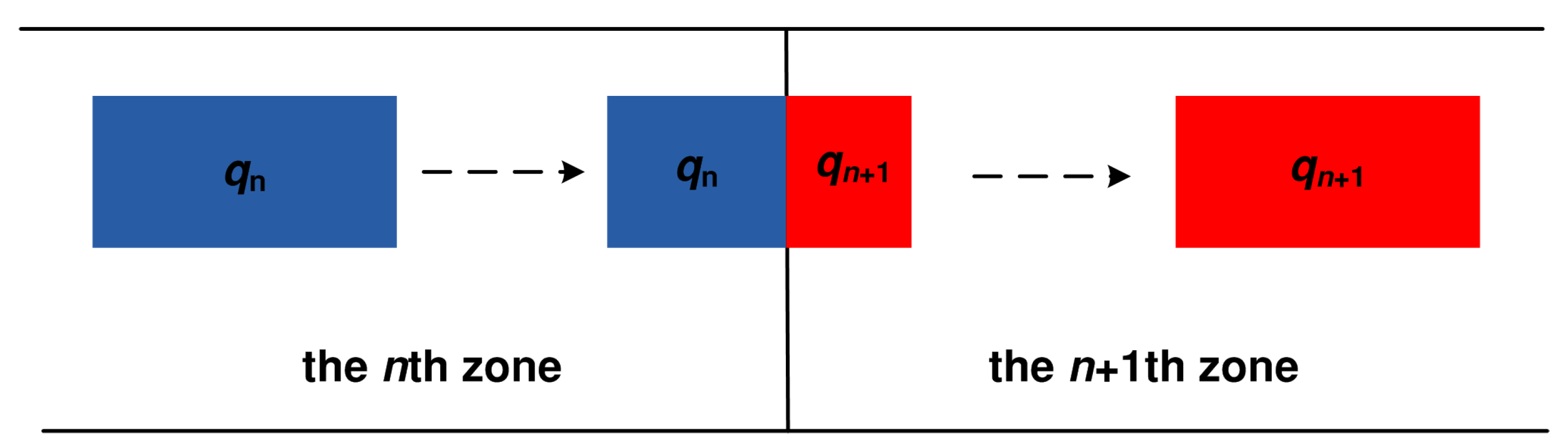
2.1. Theoretical Model for Heat Transfer during the Reflow Soldering

The reflow soldering process of the PCB assembly is implemented in a reflow oven. The reflow oven usually consists of 6–12 heating zones and one or two cooling zones. During the reflow process, the solder paste is fully melted and then rebonded in order to achieve the connection between the components and the PCB by setting different temperatures for each oven zone. Since the PCB assembly is a flat plate-shaped body which is placed in the center of the oven, the heat transfer process in each oven zone can be regarded as the heat transfer from the upper and lower surfaces of the reflow oven to the center of the PCB assembly. The heat transfer process is shown as Figure 1.
The heat transfer mode of the PCB assembly used in the reflow soldering is mainly based on heat convection and heat radiation [23,24]. According to Newton’s law of cooling, the convective heat transfer per unit area of the PCB assembly qconv can be expressed as [25]:
q conv = h c ( t w t f ) ,
where, tw is the temperature inside the oven; tf is surface temperature of the exothermic object; hc is the convective heat transfer coefficient, which is calculated by [26]:
h c = N u x λ l = 0.664 u 1 2 ( η c p ) 1 3 λ 2 3 ( υ l ) 1 2 ,
where, Nux is the Nusselt number; λ is the kinematic viscosity coefficient of the gas; l is the length of the PCB; u is the flow velocity of the gas; η is the dynamic viscosity of the gas; cp is the specific heat capacity of the gas; υ is the fluid viscosity of the gas.
Another heat transfer mode of the PCB assembly is heat radiation. The heat transfer equation per unit area of the PCB assembly qrad can be expressed as [27]:
q rad = σ ( t w 4 t f 4 ) 1 ε 1 + 1 ε 2 1 ,
where, σ is the Stefan–Boltzmann constant; ε1, ε2 are the emissivity of the heating zone and the PCB assembly, respectively.
In order to facilitate the calculation, the radiative heat transfer of the PCB assembly is always converted into convective heat transfer, namely:
q rad = σ ( t w 4 t f 4 ) 1 ε 1 + 1 ε 2 1 = h r ( t w t f ) ,
where, hr is the convective heat transfer coefficient after the conversion.
From Equation (4), hr can be calculated as:
h r = σ ε 1 ε 2 ( t w 2 + t f 2 ) ( t w + t f ) ε 1 + ε 2 ε 1 ε 2
Combining Equations (2) and (5), the total convective heat transfer coefficient h can be calculated as:
h = h c + h r
Therefore, the total heat per unit area of the PCB assembly can be expressed as:
q = h ( t w t f )

2.2. Simulation and Discussion

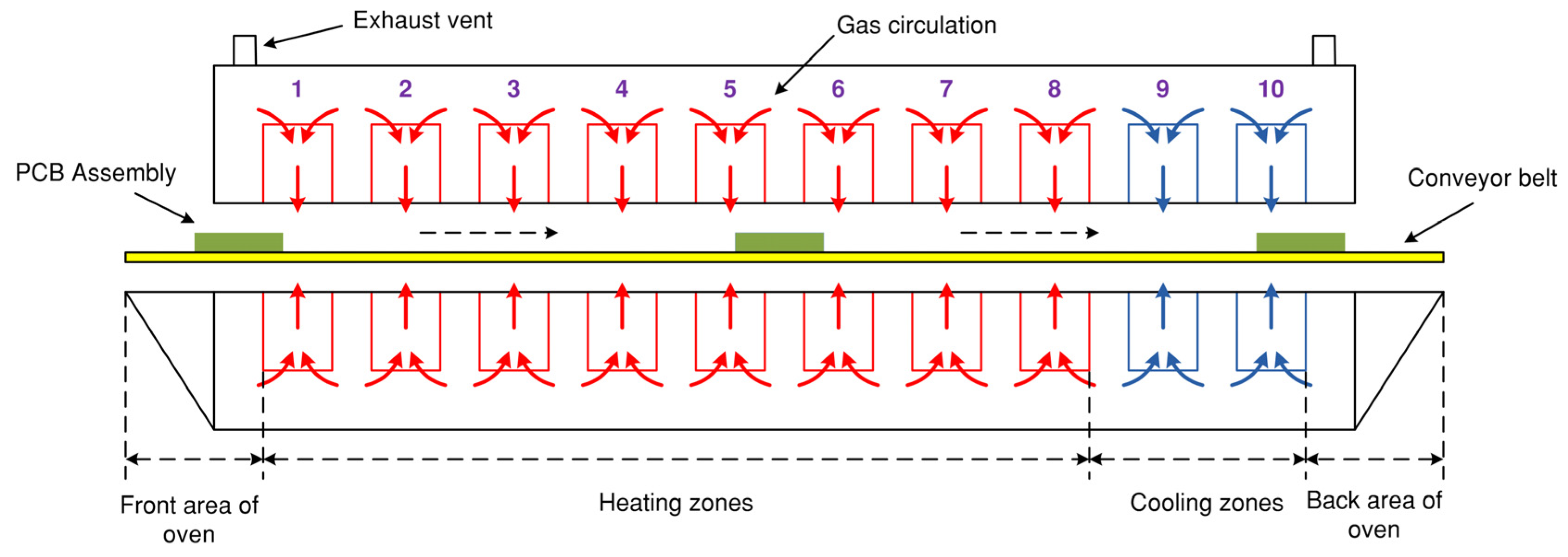
2.2.1. Finite Element Model and the Loading Process
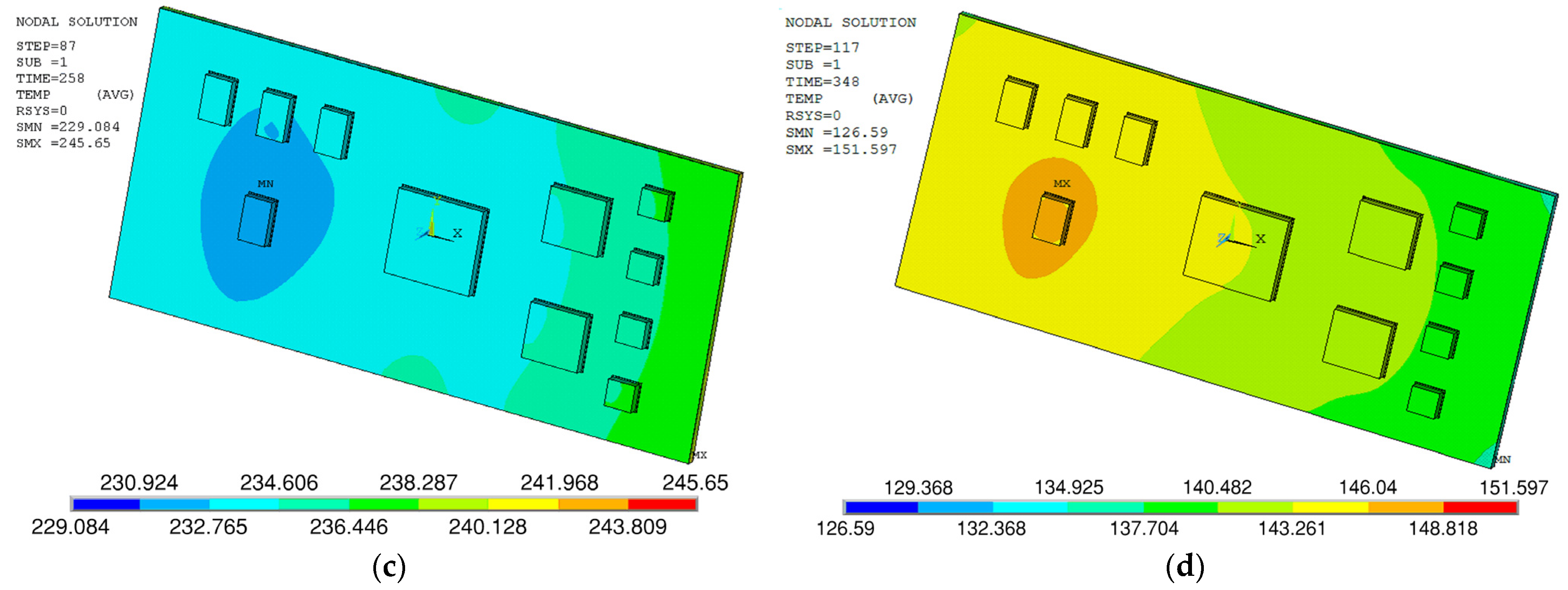
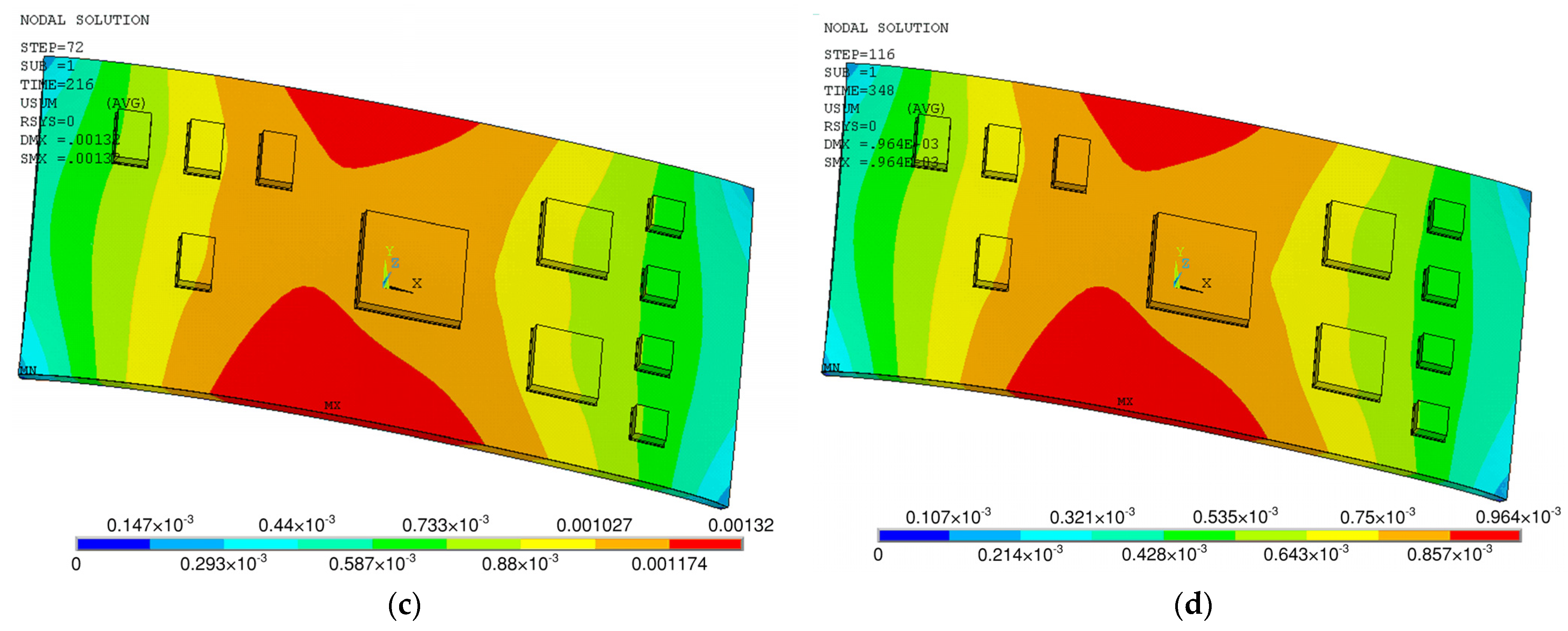
Currently, the commonly used PCB assembly mainly consists of the PCB (including the FR-4 substrate and copper foil) components in various packaging forms and the solder. Due to the complex structure of the PCB assembly, the shape and the distribution of the copper foil, the solder paste and the components in the finite element model are simplified to a certain extent for the consideration of the influence of the structural parameters on the PCB warpage. For instance, the copper foil is regarded as a layer structure and is completely attached to the entire PCB, and the solder joint under the plastic ball grid array (PBGA) is regarded as fully placed between the PCB and the PBGA. The geometric dimensions used in the modeling process, are shown in Table 1. The material properties of each component are shown in Table 2.
In this paper, an infrared convection reflow oven with 10 zones, consisting of eight heating zones and two cooling zones, is applied to simulate the reflow soldering process of the PCB assembly. The length of each zone is 500 mm and the conveyor belt speed is 850 mm/min. The temperature setting of each zone is shown in Table 3.
The coupled thermal–mechanical FEM is adopted to simulate the temperature change and warpage process on the PCB assembly during the reflow soldering. Considering that the PCB assembly passed through each zone on the conveyor belt in the reflow oven, the heat load is applied to each node on the PCB assembly by means of a moving heat source. Meanwhile, in order to prevent the relative movement of the PCB assembly on the conveyor belt, four vertices at the bottom of the PCB assembly are prevented any shifting. The schematic diagram of the loading process is shown in Figure 2. In this figure, the PCB assembly is depicted in different colors that indicate its location in the different oven zones. When the PCB assembly is completely in the nth zone, it is loaded with the heat generated in this zone (colored in blue in the figure). As the conveyor belt moves forward, part of PCB assembly enters the n + 1th zone. Due to the different temperatures in each oven zone, this part needs to be loaded with the corresponding heat of the n + 1th zone (colored in red in the figure), while the heat loaded in other parts remains the previous value. When the entire PCB assembly enters the n + 1th zone, it is loaded with the heat of the n + 1th zone.

2.2.2. Discussion

The temperature distribution on the PCB assembly during the reflow soldering is simulated using the FEM, as shown in Figure 3. It can be seen from Figure 3a that the temperature distribution is in an unbalanced state in the preheating zone because the PCB assembly enters the oven from one zone to another gradually. The heating process lasts for only a short period of time. While the PCB assembly goes into the soaking zone, it is heated for a long time in order to make the temperature distribution more uniform, and the temperature rises much more slowly than that in the preheating zone, as shown in Figure 3b. Figure 3c shows the temperature distribution of the PCB assembly in the reflow zone. Together with Table 3, it can be seen that the peak temperature will appear in this zone due to the quiet high heating temperature, which makes the solid solder paste on the PCB assembly reach its melting temperature and gradually melts to form an intermetallic compound. Following the heating process, the PCB assembly enters the cooling zone. The temperature in this zone is quite low, which leads to a rapid drop in temperature in the PCB assembly. Simultaneously, the melted solder pastes in the reflow zone resolidify in order to form the connection between the component and the PCB, as shown in Figure 3d.
The warpage on the PCB assembly during the reflow soldering is studied based on the temperature field simulation, as shown in Figure 4. From Figure 4a, the amount of warpage grows from 0 mm to 0.419 mm when the PCB assembly passes through the preheating zone. Since the temperature rises rapidly in the preheating zone and the thermal conductivity of each component is different, a large temperature difference appears at each position of the PCB assembly, thereby causing the deformation. When the PCB assembly passes through the soaking zone, the amount of warpage increases from 0.419 mm to 0.91 mm. During this period, although the differences in the material properties of each component increase further, the warpage rate is reduced due to a sufficiently long soaking time, the low heating rate and the relatively uniform temperature distribution, as shown in Figure 4b. When the PCB assembly enters the reflow zone, the difference of the material properties (especially the CTE) among the components rises to the maximum as the temperature reaches its peak value, thereby resulting in the highest amount of warpage at 1.32 mm, as shown in Figure 4c. Finally, the PCB assembly enters the cooling zone. Due to the rapid temperature drop in this zone, the difference in the material properties of each component gradually decreases, and the amount of warpage also decreases from its maximum value to 0.964 mm, as shown in Figure 4d.
From Figure 3 and Figure 4, it can be concluded that the warpage and temperature field have similar trends, which are manifested as the nonlinear increase in the amount of warpage with the increase in temperature on the PCB assembly. The higher the temperature, the greater the amount of warpage. Furthermore, the faster the heating rate rises, the faster the warpage rate occurs.
Figure 5 shows the displacement of the components (FR-4, copper foil, solder and PBGA) on the PCB assembly over time. From Figure 5, the PCB assembly has a certain displacement in the X, Y, and Z directions during the reflow soldering process. Meanwhile, the displacement in the Z direction is much greater than the other two directions. On this basis, it can be considered that the displacement in the Z direction is the main cause of warpage.

2.2.3. Calculation of the Warpage Percentage for the PCB Assembly

The allowable warpage percentage for the PCB assembly has been specified by international industrial standards IPC-A-600G [28]. The standard stipulates that the maximum warpage percentage of the board assembly is 0.75%. Furthermore, the allowable warpage percentage in the electronic assembly factories is usually 0.70~0.75%. On this basis, the allowable warpage percentage [Q] used in this study is set to 0.75%.
From the international industrial standard IPC-TM-650 [29], the warpage percentage for the PCB assembly Q is calculated as follows:
Q = w L × 100 % ,
where, w is the height of warpage; L the length of PCB assembly.
The amount of warpage along the Z direction is measured in the finite element simulation. Then, the warpage percentage is calculated as well and the results are shown in Figure 6. The figure shows that the final warpage percentage is 0.713%, which is lower than the allowable value as the reflow parameters are set to the values in Table 3. Therefore, the reflow parameters in this study well meet the requirements regarding warpage on the PCB assembly in engineering.

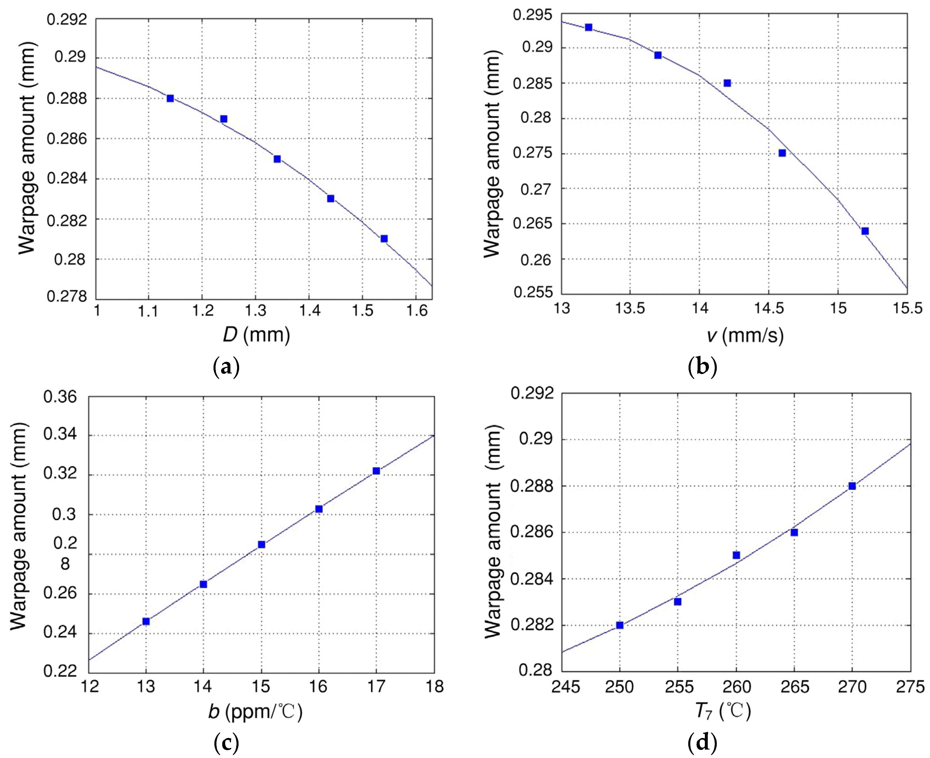
2.2.4. Analysis of the Factors Affecting Warpage

From the above analysis, the main factors that cause warpage on the PCB assembly are the differences in the CTE among the different components and the highest temperature in the reflow zone. On the other hand, the amount of time the PCB assembly spends in each oven zone and the PCB thickness also have significant impacts on warpage [13,30]. Therefore, the main factors affecting warpage are determined as the conveyor belt speed v, the temperature in the 7th oven zone T7, the PCB thickness D and the CTE of the PCB b. The effect of these different factors on warpage is shown in Figure 7.
Figure 7 shows that the warpage decreases with the increase of D and v, but increases as b and T7 grow. Firstly, the increase in the PCB thickness not only improves its bending stiffness, but also accelerates its heat dissipation effect in the cooling zone, so the warpage is reduced as the PCB thickness increases. Secondly, as the conveyor belt speeds up, the PCB assembly stays in the reflow zone for a shorter period of time, which results in a reduction in the amount of time that the PCB is above Tg. Thus, warpage is reduced in turn. Thirdly, when the CTE of the PCB increase, the mismatch of the CTE among the components becomes more prominent, thereby leading to a larger amount of warpage. Last but not the least, when temperature in the 7th oven zone increases, the peak temperature of the PCB assembly also increases. This may increase the difference in the material properties among the components and even cause an increase in the warpage.

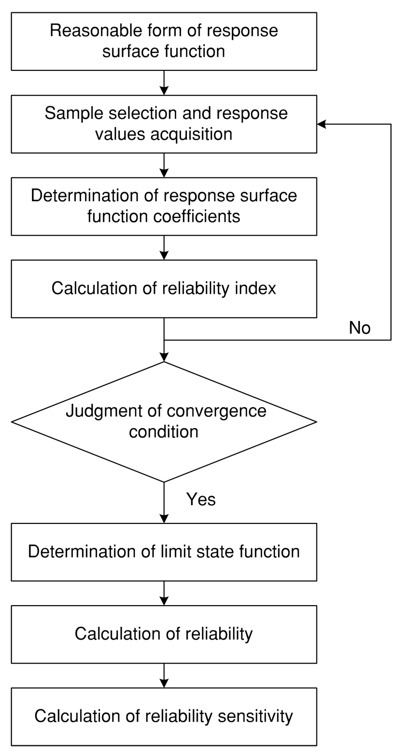
3. Reliability Sensitivity of the PCB Assembly concerning Warpage

3.1. Limit State Function Based on the RSM

As can be seen from the previous study, the warpage on the PCB assembly is affected by a number of influencing factors, which have randomness inevitably. Therefore, the amount of warpage can be described by the limit state function. According to the concept of structural reliability, when the structural reliability is affected by n random variables, the structural function can be expressed as [31]:
z = g ( X 1 , X 2 , , X n ) ,
where, Xi (i = 1, 2, …, n) are the random variables of the structural reliability; g(X) is the limit state function. Whether the functional state of the structure fails, is judged according to the value of the limit state function. That is, when g(X) > 0, the structure is in a reliable state; when g(X) = 0, the structure is in a limited state; when g(X) < 0, the structure is in a failure state.
In practical engineering, the relationship between the input and output of random variables is usually highly nonlinear due to the very complex factors that affect the state of the structure. Therefore, the explicit expression of the limit state function cannot be directly deduced in a reliability analysis. The RSM is beneficial to solve this type of problem [32].
Since the RSM describes an approximate relationship between a set of independent variables and the system response, Equation (10) is usually applied to describe the relationship between variables and responses:
y ( x ) = y ^ ( x ) + ε ,
where, y(x) is the actual value of the response surface, which is an unknown function; ε is the random error between the approximate value and the actual value, which usually obeys the standard normal distribution of (0, σ2); y ^ ( x ) is the approximate value of the response, usually a quadratic polynomial, which can be expressed as:
y ^ ( x ) = β 0 + i 1 n β i x i + i 1 n β i x i 2 + 1 i j n β i j x i x j ,
where, βi is the polynomial coefficient.
Assuming that the maximum allowable amount of warpage on the PCB assembly is lmax, the limit state function g(X) deduced by RSM is:
g ( X ) = l max y ^ ( x ) = l max ( β 0 + i 1 n β i x i + i 1 n β i x i 2 + 1 i j n β i j x i x j )

3.2. Reliability Calculation

When the random variables in Equation (12) are independent of each other, their mean matrix and variance matrix can be expressed as μ = [μ1, μ2,…, μn] and D = [D1, D2,…, Dn], then there are:
E ( X i 2 ) = E 2 ( X i ) + D ( X i ) = μ i 2 + D i ,
E ( X i X j ) = E ( X i ) E ( X j ) = μ i μ j ,
D ( X i 2 ) = 4 μ i 2 D i + 2 D i ,
D ( X i X j ) = μ i 2 D j + μ j 2 D i + D i D j
So that the mean and variance of g(X) are:
E [ g ( X ) ] = μ g ( μ 1 , μ 2 , , μ n , D 1 , D 2 , , D n ) ,
D [ g ( X ) ] = D g ( μ 1 , μ 2 , , μ n , D 1 , D 2 , , D n )
Therefore, the reliability index β can be expressed as:
β = μ g D g
If g(X) obeys a normal distribution, the reliability R is:
R = Φ ( β ) ,
where, Φ(•) is the standard normal distribution function.

3.3. Calculation of Reliability Sensitivity

The reliability sensitivity to the mean matrix μ and variance matrix D of the random variables vector is:
R μ T = R β ( β μ g μ g μ T + β D g D g μ T ) ,
R D T = R β ( β μ g μ g D T + β D g D g D T ) ,
where,
{ R β = φ ( β ) β μ g = 1 D g β D g = μ g 2 D g 3 2 μ g μ T = [ μ g μ 1 , μ g μ 2 , , μ g μ n ] T μ g D T = [ μ g D 1 , μ g D 2 , , μ g D n ] T D g μ T = [ D g μ 1 , D g μ 2 , , D g μ n ] T D g D T = [ D g D 1 , D g D 2 , , D g D n ] T
The flowchart for the proposed model is shown in Figure 8.

3.4. Case Study

It can be seen that the warpage on the PCB assembly is chiefly affected by v, T7, D and b. Moreover, randomness appears on these parameters due to uncertain reasons. Therefore, they can be defined as random variables. Assuming that the above random variables follow the normal distribution, the mean and standard deviation are shown in Table 4.
When the probability levels are p1 = 0.01, p2 = 0.50 and p3 = 0.99, respectively, the sample values of the random input variables obtained according to the Box–Behnken design method are listed in Table 5.
The finite element simulation is applied to calculate 25 response values of the warpage amount with the data in Table 5. Then, the response surface function can be deduced according to these response values combined with Equation (11) as:
y ^ = 0.6344 + 0.0677 v 0.0068 T 7 0.6136 D + 0.0601 b 0.0068 v 2 0.0897 D 2 0.0032 b 2 + 0.0005 v T 7 0.0045 v D 0.0014 v b + 0.0002 T 7 D 0.0001 T 7 b + 0.0496 D b
Since the international standard has stipulated that the warpage percentage on the qualified PCB assembly can be no more than 0.75%, the maximum allowable warpage in this case is lmax = 0.8925 mm. Therefore, according to Equation (12), the limit state function of warpage on the PCB assembly can be expressed as:
g ( X ) = l max y ^ = 0.2581 0.0677 v + 0.0068 T 7 + 0.6136 D 0.0601 b + 0.0068 v 2 + 0.0897 D 2 + 0.0032 b 2 0.0005 v T 7 + 0.0045 v D + 0.0014 v b 0.0002 T 7 D + 0.0001 T 7 b 0.0496 D b
It is assumed that the 25 warpage amounts obey a normal distribution. Since the sample size is small, the K–S method is applied for the hypothetical test. The test result shows that the warpage amounts obey the normal distribution with the mean μ = 0.2826 and the standard deviation σ = 0.01763. Therefore, the reliability and sensitivity of the PCB assembly concerning warpage can be calculated directly using the limit state function.
The mean of the limit state function can be expressed as follows with the help of Equations (13), (14) and (17):
μ g = E [ g ( X ) ] = 0.2581 0.0667 μ v + 0.0068 μ T 7 + 0.6136 μ D 0.0601 μ b + 0.0068 ( μ v 2 + D v ) + 0.0897 ( μ D 2 + D D ) + 0.0032 ( μ b 2 + D b ) 0.0005 μ v μ T 7 + 0.0045 μ v μ D + 0.0014 μ v μ b 0.0002 μ T 7 μ D + 0.0001 μ T 7 μ b 0.0496 μ D μ b
The variance of the limit state function can be deduced with Equations (15), (16) and (18) as:
D g = D [ g ( X ) ] = 0.0677 2 D v + 0.0068 2 D T 7 + 0.6136 2 D D + 0.0601 2 D b + 0.0068 2 ( 4 μ v 2 D v + 2 D v ) + 0.0897 2 ( 4 μ D 2 D D + 2 D D ) + 0.0032 2 ( 4 μ b 2 D b + 2 D b ) + 0.0005 2 ( μ v 2 D T 7 + μ T 7 2 D v + D v D T 7 ) + 0.0045 2 ( μ v 2 D D + μ D 2 D v + D v D D ) + 0.0014 2 ( μ v 2 D b + μ b 2 D v + D v D b ) + 0.0002 2 ( μ T 7 2 D D + μ D 2 D T 7 + D E D D ) + 0.0001 2 ( μ T 7 2 D b + μ b 2 D T 7 + D T 7 D b ) + 0.0496 2 ( μ D 2 D b + μ b 2 D D + D D D b )
Hence, the reliability of the PCB assembly with Equations (19) and (20) is:
R = 0.9907
By means of the above calculation, the reliability sensitivity of the PCB assembly is calculated accompanied with Equations (21) and (22), namely:
R μ T = [ R μ v R μ T 7 R μ D R μ b ] T = [ 0.001396 0.0003865 0.003320 0.003215 ]
R D T = [ R D v R D T 7 R D D R D b ] T = [ 0.0273 0.00004306 0.4272 0.0034 ]
From the reliability sensitivity to the mean matrix of the random variable vector R μ T , it can be seen that the increase of the mean of T7 and b improve the reliability, while the increase of the mean of v and D reduce the reliability. Moreover, the reliability is more sensitive to the mean of D and b. From the reliability sensitivity to the variance matrix of the random variable vector R D T , it can be seen that the increases in the variance of all of the random variables reduce the reliability. Moreover, the reliability sensitivity to the variance of D is the greatest.
In general, the above reliability sensitivity results are consistent with the analysis of the influencing factors of warpage on the PCB assembly, which is shown in Figure 7. It confirms that the reliability sensitivity analysis method and conclusion are effective. Therefore, it can be concluded that the reliability sensitivity analysis can provide a theoretical basis for the reliability design and optimization of the PCB assembly concerning warpage in the reflow soldering process.
The engineering significance of the reliability sensitivity analysis on the PCB assembly lies in: (1) The reliability of the PCB assembly concerning warpage is calculated using the influence of multiple factor random errors. Not only does the research provide a clear understanding of the random error impact on the PCB assembly reliability from a theoretical perspective for engineers, but it also provides a reasonable limit regarding the random error range of the parameters. Simultaneously, the yield of the PCB assembly can be effectively predicted through mass production. (2) The influence law and degree of each factor on warpage can be determined using the reliability sensitivity analysis. Engineers can improve the reliability by adjusting the parameters with greater influence during the structural design and the process formulation stages. Although this study only analyzes the effects of four factors in the material properties, the geometric dimensions and process parameters on warpage, the advanced method can support the analysis of other factors. In addition, it should be noted that the reliability sensitivity method is also applicable to the analysis of other failure modes that occur on the PCB assembly.

4. Conclusions

Aiming at providing a theoretical basis for the effective control of warpage occurring on the PCB assembly during the reflow soldering process, the FEM and the reliability sensitivity analysis are applied to revealing the influence of the geometric dimensions, the material properties and the process parameters on warpage, and exploring the effects on the reliability of multiple factor random errors. The main conclusions are as follows:
(1)
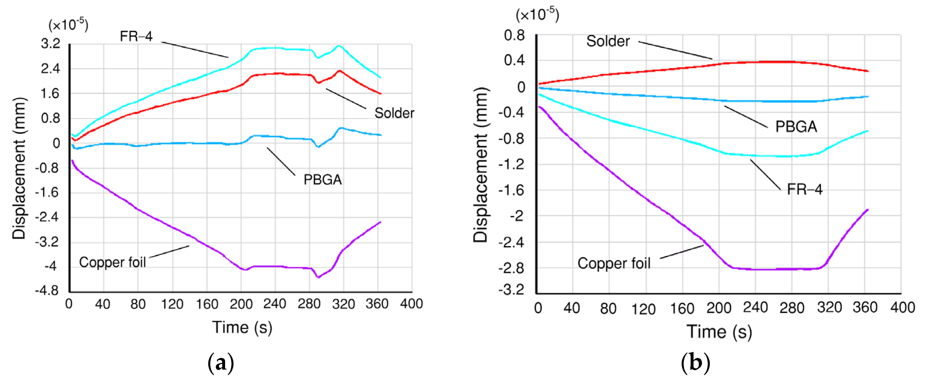
The coupled thermal-mechanical FEM was applied to simulating the temperature change and warpage process during the reflow soldering on the PCB assembly. The results showed that the warpage had a similar trend to that of the temperature change. Specifically, the amount of warpage increased nonlinearly with the increase of PCB assembly temperature. There was a significant rise in the warpage rate with the increasing heating rate;
(2)
By means of the limit state function, the reliability on the PCB assembly concerning warpage with the influence of multiple factor random errors was 0.9907. The calculation method can provide a theoretical guidance for the limitation of the allowable error range of the material properties, the geometric dimensions and the process parameters, which are beneficial to reduce the possibility of warpage failure on the PCB assembly during the reflow soldering process;
(3)
The reliability sensitivity analysis of the PCB assembly showed that the mean and variance of each parameter had varying degrees of influence on the reliability. The reliability improved as the mean of PCB thickness and conveyor belt speed increased while it decreased as the mean of the CTE of the PCB and the temperature in the 7th oven zone increased. Among others, the PCB thickness had the greatest impact on reliability. Meanwhile, an increase in the variance of all parameters reduced the reliability.

Author Contributions

Conceptualization, Y.G. and M.L.; methodology, Y.G. and M.L.; software, Y.G., M.L. and M.Y.; validation, Y.G. and M.Y.; formal analysis, M.L.; investigation, Y.G.; resources, M.L. and Y.Y; data curation, Y.G. and M.L.; writing—original draft preparation, Y.G. and M.L.; writing—review and editing, Y.G. and M.L.; visualization, Y.G. and M.Y.; supervision, Y.Y.; project administration, Y.G. and Y.Y.; funding acquisition, Y.G., M.L. and Y.Y. All authors have read and agreed to the published version of the manuscript.

Funding

This research was funded by National Natural Science Foundation of China, grant number 51875095 and 51705342, and Scientific Research Funding of Educational Department of Liaoning Province, China, grant number LJKZ0003 and LJKZ0574.

Institutional Review Board Statement

Not applicable.

Informed Consent Statement

Not applicable.

Data Availability Statement

The data presented in this study are available upon request from the corresponding authors.

Conflicts of Interest

The authors declare no conflict of interest.

References

  1. Lau, C.S.; Khor, C.Y.; Soares, D.; Teixeira, F.C.; Abdullah, M.Z. Thermo-mechanical challenges of reflowed lead-free solder joints in surface mount components: A review. Solder. Surf. Mt. Technol. 2016, 28, 41–62. [Google Scholar] [CrossRef]
  2. Chen, L.M.; Li, E.Y.; Wang, H. Time-based reflow soldering optimization by using adaptive Kriging-HDMR method. Solder. Surf. Mt. Technol. 2016, 28, 101–113. [Google Scholar] [CrossRef]
  3. Geczy, A.; Fejos, M.; Tersztyanszky, L.; Kemler, A.; Szabo, A. Investigating printed circuit board shrinkage during reflow soldering. In Proceedings of the 37th International Spring Seminar on Electronics Technology 2014, Dresden, Germany, 7–11 May 2014; pp. 219–224. [Google Scholar] [CrossRef]
  4. Geczy, A.; Fejos, M.; Tersztyanszky, L. Investigating and compensating printed circuit board shrinkage induced failures during reflow soldering. Solder. Surf. Mt. Technol. 2015, 27, 61–68. [Google Scholar] [CrossRef]
  5. Addagarla, A.; Prasad, N.S. Finite element analysis of flip–chip on board (FCOB) assembly during reflow soldering process. Solder. Surf. Mt. Technol. 2012, 24, 92–99. [Google Scholar] [CrossRef]
  6. Lau, C.S.; Tan, C.Y.; Le, C.K.; Ye, N. A numerical technique to evaluate warpage behavior of double sided rigid-flex board assemblies during reflow soldering process. In Proceedings of the 70th IEEE Electronic Components and Technology Conference, Orlando, FL, USA, 3–30 June 2020; pp. 554–560. [Google Scholar] [CrossRef]
  7. Kang, J.S. Parametric study of warpage in PBGA packages. Int. J. Adv. Manuf. Technol. 2020, 107, 4213–4219. [Google Scholar] [CrossRef]
  8. Liu, C.W.; Li, M.; Lu, J.C.; Gao, L.M. A new approach to minimize package warpage in reflow process. In Proceedings of the 18th International Conference on Electronic Packaging Technology, Harbin, China, 16–19 August 2017; pp. 988–991. [Google Scholar]
  9. Ding, H.; Ume, I.C.; Powell, R.E.; Hanna, C.R. Parametric study of warpage in printed wiring board assemblies. IEEE Trans. Compon. Packag. Technol. 2005, 28, 517–524. [Google Scholar] [CrossRef]
  10. Tan, W.; Ume, I.C. Application of lamination theory to study warpage across PWB and PWBA during convective reflow process. IEEE Trans. Compon. Pack. Manuf. Technol. 2012, 2, 217–223. [Google Scholar] [CrossRef]
  11. Wang, T.H.; Tsai, C.I.; Lee, C.C.; Lai, Y.S. Study of factors affecting warpage of HFCBGA subjected to reflow soldering-liked profile. Microelectron. Reliab. 2013, 53, 297–302. [Google Scholar] [CrossRef]
  12. Xia, W.S.; Xiao, M.; Chen, Y.H.; Wu, F.S.; Liu, Z.; Fu, H.Z. Thermal warpage analysis of PBGA mounted on PCB during reflow process by FEM and experimental measurement. Solder. Surf. Mt. Technol. 2014, 26, 162–171. [Google Scholar] [CrossRef]
  13. Chung, S.; Kwak, J.B. Realistic warpage evaluation of printed board assembly during reflow process. Solder. Surf. Mt. Technol. 2015, 27, 137–145. [Google Scholar] [CrossRef]
  14. Jafari-Asl, J.; Ohadi, S.; Ben Seghier, M.E.A.; Trung, N.-T. Accurate structural reliability analysis using an improved line-sampling-method-based slime mold algorithm. ASCE-ASME J. Risk. Uncertain. Eng. Syst. Part A-Civ. Eng. 2021, 7, 04021015. [Google Scholar] [CrossRef]
  15. Cornebize, T.; Legrand, A. Simulation-based optimization and sensibility analysis of MPI applications: Variability matters. J. Parallel Distrib. Comput. 2022, 166, 111–125. [Google Scholar] [CrossRef]
  16. Rashki, M.; Moghaddam, M.A.; Miri, M. System-level reliability sensitivity analysis by using weighted average simulation method. Qual. Reliab. Eng. Int. 2019, 35, 1826–1845. [Google Scholar] [CrossRef]
  17. Zhai, X.; Fei, C.W.; Zhai, Q.G.; Wang, J.J. Reliability and sensitivity analyses of HPT blade-tip radial running clearance using multiply response surface model. J. Cent. South Univ. 2014, 21, 4368–4377. [Google Scholar] [CrossRef]
  18. Guo, W.; Cui, W.M.; Yu, T.X.; Song, B.F. The reliability and sensibility analysis for an aircraft lock mechanism based on the surrogate models. In Proceedings of the ASME International Mechanical Engineering Congress and Exposition, Houston, TX, USA, 13–19 November 2015; Volume 14, pp. 1–9. [Google Scholar] [CrossRef]
  19. Zhang, T.X.; Zhang, Y.M. A new model for reliability design and reliability sensitivity analysis of a hydraulic piston pump. Proc. Inst. Mech. Eng. Part O-J. Risk Reliab. 2017, 231, 11–24. [Google Scholar] [CrossRef]
  20. Lu, C.; Feng, Y.W.; Liem, R.P.; Fei, C.W. Improved Kriging with extremum response surface method for structural dynamic reliability and sensitivity analyses. Aerosp. Sci. Technol. 2018, 76, 164–175. [Google Scholar] [CrossRef]
  21. Maizia, A.; Hocine, A.; Dehmous, H.; Chapelle, D. Prediction of reliability analysis of composite tubular structure under hygro-thermo-mechanical loading. Mech. Adv. Mater. Struct. 2019, 26, 372–379. [Google Scholar] [CrossRef]
  22. Rad, M.J.G.; Ohadi, S.; Jafari-Asl, J.; Vatani, A.; Ahmadabadi, S.A.; Correia, J.A.F.O. GNDO-SVR: An efficient surrogate modeling approach for reliability-based design optimization of concrete dams. Structures 2022, 35, 722–733. [Google Scholar] [CrossRef]
  23. Illes, B. Measuring heat transfer coefficient in convection reflow ovens. Measurement 2010, 43, 1134–1141. [Google Scholar] [CrossRef]
  24. Xu, Y.Z.; Liu, Y.; Zhang, L. Effects of the solder phase transformation on the optimization of reflow soldering parameters and temperature profiles. Discrete Dyn. Nat. Soc. 2021, 2021, 9955967. [Google Scholar] [CrossRef]
  25. Srivalli, C.; Abdullah, M.Z.; Khor, C.Y. Numerical investigations on the effects of different cooling periods in reflow-soldering process. Heat Mass Transf. 2015, 51, 1413–1423. [Google Scholar] [CrossRef]
  26. Lei, Q.Y.; Zhang, Z.Y.; Zhuo, S.Y.; Lin, K.J. Research on furnace temperature curve based on heat convection and heat radiation. In Proceedings of the 2nd International Academic Exchange Conference on Science and Technology Innovation, Guangzhou, China, 18–20 December 2020; Volume 233, p. 04004. [Google Scholar] [CrossRef]
  27. Ma, G.; Huang, X.Q.; Liu, S.H. Heat transfer modeling and oven temperature curve optimization of integrated circuit board reflow soldering. IEEE Access 2021, 9, 141876–141889. [Google Scholar] [CrossRef]
  28. IPC-A-600G; Acceptability of Printed Boards. The Institute for Interconnecting and Packaging Electronic Circuits: Bannockburn, IL, USA, 2004.
  29. IPC-TM-650; Test Methods Manual. The Institute for Interconnecting and Packaging Electronic Circuits: Northbrook, IL, USA, 2020.
  30. Aziz, M.S.A.; Abdullah, M.Z.; Khor, C.Y.; Azid, I.A.; Jalar, A.; Ani, F.C. Influence of printed circuit board thickness in wave soldering. Sci. Iran. 2017, 24, 2963–2976. [Google Scholar] [CrossRef]
  31. Li, X.L.; Chen, G.H.; Cui, H.C.; Yang, D.X. Direct probability integral method for static and dynamic reliability analysis of structures with complicated performance functions. Comput. Meth. Appl. Mech. Eng. 2021, 374, 113583. [Google Scholar] [CrossRef]
  32. Li, P.; Li, H.Y.; Huang, Y.B.; Wang, K.F.; Xia, N. Quasi-sparse response surface constructing accurately and robustly for efficient simulation based optimization. Adv. Eng. Softw. 2017, 114, 325–336. [Google Scholar] [CrossRef]
Figure 1. Schematic diagram of the heat transfer during the reflow soldering.
Mathematics 10 03055 g001
Figure 2. Loading process of the moving heat source on the PCB assembly.
Mathematics 10 03055 g002
Figure 3. Temperature distribution of the PCB assembly during the reflow soldering. (a) Preheating zone. (b) Soaking zone. (c) Reflow zone. (d) Cooling zone.
Mathematics 10 03055 g003aMathematics 10 03055 g003b
Figure 4. Warpage process on the PCB assembly. (a) Preheating zone. (b) Soaking zone. (c) Reflow zone. (d) Cooling zone.
Mathematics 10 03055 g004aMathematics 10 03055 g004b
Figure 5. Displacements of the components along the different directions over time. (a) X direction. (b) Y direction. (c) Z direction.
Mathematics 10 03055 g005aMathematics 10 03055 g005b
Figure 6. Warpage percentage at different times.
Mathematics 10 03055 g006
Figure 7. Analysis of the factors that influence warpage. (a) PCB thickness. (b) Conveyor belt speed. (c) CTE of PCB. (d) Temperature in the 7th oven zone.
Mathematics 10 03055 g007
Figure 8. Flowchart for the model.
Mathematics 10 03055 g008
Table 1. Geometric dimensions of the PCB assembly.
PartMaterialSize (mm)Quantity
PCBFR-4100 × 65 × 1.341
Copper foil100 × 65 × 0.071
SolderSn-Ag-Cu5.5 × 5.5 × 0.154
5.5 × 8.5 × 0.154
10.5 × 10.5 × 0.152
15.5 × 15.5 × 0.151
ComponentSi5 × 5 × 1.54
5 × 8 × 1.54
PBGA10 × 10 × 1.52
15 × 15 × 1.51
Table 2. Material properties of each component.
MaterialDensity
(kg/m3)
Specific Heat (J/kg·K)Thermal Conductivity (W/m·K)Elastic Modulus (Gpa)Poisson RatioCTE
(ppm/°C)
FR-418208400.2930 °C: 22.4
95 °C: 20.68
150 °C: 17.92
0.3927 °C: 13.62
37 °C: 14.19
47 °C: 14.77
57 °C: 16.38
130 °C: 31.62
220 °C: 73.6
Copper foil8893265.47 + 0.31T469.95 + 0.1761T760.3517
Solder74003013360.73 − 0.06T0.3623.9 + 0.02 T
Silicon die233027 °C: 713
127 °C: 785
227 °C: 832
27 °C: 156
127 °C: 105
227 °C: 80
1670.325 °C: 2.6
100 °C: 3.1
225 °C: 3.6
BT substrate300015706517.80.15<215 °C: 35.0
>215 °C: 140
Table 3. Temperature setting in different zones.
ZonePreheating ZoneSoaking ZoneReflow ZoneCooling Zone
T1T2T3T4T5T6T7T8T9T10
Temperature (°C)1601651801852052402602306020
Table 4. Mean and standard deviation of each variable.
Variablev (mm/s)T7 (°C)D (mm)b (ppm/°C)
Mean14.22601.3415
Standard deviation0.250.050.5
Table 5. Samples of Box–Behnken method and response values.
No.v (mm/s)T7 (°C)D (mm)b (ppm/°C)l (mm)
LevelValueLevelValueLevelValueLevelValue
1p214.2p2260p21.34p2150.285
2p113.734p1248.35p21.34p2150.297
3p314.666p1248.35p21.34p2150.269
4p113.734p3271.65p21.34p2150.292
5p314.666p3271.65p21.34p2150.274
6p214.2p2260p11.22p113.8350.265
7p214.2p2260p31.46p113.8350.261
8p214.2p2260p11.22p316.1650.310
9p214.2p2260p31.46p316.1650.305
10p113.734p2260p21.34p113.8350.267
11p314.666p2260p21.34p113.8350.251
12p113.734p2260p21.34p316.1650.312
13p314.666p2260p21.34p316.1650.293
14p214.2p1248.35p11.22p2150.285
15p214.2p3271.65p11.22p2150.290
16p214.2p1248.35p31.46p2150.280
17p214.2p3271.65p31.46p2150.286
18p113.734p2260p11.22p2150.292
19p314.666p2260p11.22p2150.274
20p113.734p2260p31.46p2150.288
21p314.666p2260p31.46p2150.271
22p214.2p1248.35p21.34p113.8350.250
23p214.2p3271.65p21.34p113.8350.265
24p214.2p1248.35p21.34p316.1650.294
25p214.2p3271.65p21.34p316.1650.310
Publisher’s Note: MDPI stays neutral with regard to jurisdictional claims in published maps and institutional affiliations.

