Article

Evolutionary Synthesis of Failure-Resilient Analog Circuits

Faculty of Electrical Engineering, University of Ljubljana, Tržaška cesta 25, SI-1000 Ljubljana, Slovenia
*
Author to whom correspondence should be addressed.
Mathematics 2022, 10(1), 156; https://doi.org/10.3390/math10010156
Submission received: 26 November 2021 / Revised: 22 December 2021 / Accepted: 2 January 2022 / Published: 5 January 2022
(This article belongs to the Special Issue Optimization Theory and Applications)

Abstract

:
Analog circuit design requires large amounts of human knowledge. A special case of circuit design is the synthesis of robust and failure-resilient electronics. Evolutionary algorithms can aid designers in exploring topologies with new properties. Here, we show how to encode a circuit topology with an upper-triangular incident matrix and use the NSGA-II algorithm to find computational circuits that are robust to component failure. Techniques for robustness evaluation and evolutionary algorithm guidances are described. As a result, we evolve square root and natural logarithm computational circuits that are robust to high-impedance or short-circuit malfunction of an arbitrary rectifying diode. We confirm the simulation results by hardware circuit implementation and measurements. We think that our research will inspire further searches for failure-resilient topologies.

1. Introduction

Although most signal processing is shifting to the digital domain, some functions still require analog solutions, typically on the interfaces between a digital processor and the physical world [1,2]. This includes, but is not limited to, various types of amplifiers, sensors, signal transmitters and receivers, actuators, and high-speed and low-power processors. Analog circuit design is expensive: it requires teams of high-profile electronics designers who must usually under pressure to achieve high performance requirements with short time-to-market expectations. When customer requirements involve various degrees of circuit robustness, the task becomes even harder. Engineers often use statistical strategies, such as Monte Carlo analysis, in order to predict the circuit manufacturability and production yield [3]. Those methods, however, address the problem of circuit usability after fabrication because different production methods have their own technological uncertainties, for example, component tolerances, parasitics, lithography resolution, mask displacement, etc. Usually, designers also consider simulations of the environmental effects on the electronics, such as ambient temperature and humidity, because these effects generally contribute to circuitry behavior.
Analog circuit design becomes particularly challenging when the device is targeted for use under harsh conditions, such as space exploration, aeronautical and military missions, tactical robotics etc. Such situations might include extreme temperature swings, high ionizing and electromagnetic radiation levels, high working electrical currents, and more. In such cases, electronic devices undergo extreme stress, which can result in component faults and, consequently, to mission failure.
Researchers and engineers have invested considerable effort to protect electronic devices against such failures. The canonical methods of hardening the electronics include overdesign, additional shielding and insulation, and thermal managing, which all significantly increase the final cost and weight of a device. These methods try to prevent failuresper se. That said, device failures can still occur in vivo, for example, because of high working currents [4]. Engineers often solve this problem using duplicated circuit modules to form redundant subsystems in combination with voting mechanisms [5,6]. As such, the demultiplexer becomes a weak point of the system. Some approaches also include active in situ compensation techniques, where a complex adjustment mechanism then becomes a single point of potential failure.
In this study, we focused on an alternative approach to providing circuit robustness. We used an exhaustive evolutionary search to find circuit topologies resilient to semiconductor component failures. By resilient, we mean that circuits show minimal performance degradation, if anyof the semiconductor devices fails. We modeled component failures in both a stuck-short and stuck-open situation. The resulting circuits are robusta priori and do not include any external mitigation techniques.
Our results include nonlinear computational analog circuits, such as square root and natural logarithm computing circuits, which are rather robust to any semiconductor diode short-circuit and high-impedance malfunctions. To the best of our knowledge, this is one of the few published works on automated synthesis of a priori robust, failure-resilient nonlinear computational analog circuits [5,6,7,8,9,10,11,12,13,14,15,16,17,18]. Additionally, we confirmed our results in a hardware implementation.
The paper is organized as follows: In Section 1.1, we briefly review the existing techniques for analog circuit topology synthesis with a focus on robust topology design. Our motivation for improvement in the field is described in Section 1.2. In Section 2, the synthesis methods are explained in detail. We provide our research results in Section 3. A discussion concludes this paper in Section 3.4.

1.1. Previous Work on Evolutionary Robust-Design for Analog Circuits

Robust design is a key challenge in many engineering areas. Many researchers have attempted to design processes, protocols, topologies, and devices that can survive total component failures. In addition to electronics engineering, such studies can also be found in fields of robust mechanical engineering and robotics [19], control systems [20,21], power engineering [22], and others.
Analog circuit synthesis was also addressed by many researchers. In this section we briefly review works, correlated to a problem of robust analog circuit synthesis.

1.1.1. Analog Circuit Synthesis

For more than a century, discoveries of novel circuit designs have occurred in the exclusive domain of human experts. This might change with the advent of sophisticated circuit synthesis tools, relying on AI [23]. Since the beginning of this intriguing research field [24,25,26], the results of computer-aided topology syntheses have increasingly become human-competitive and trustworthy for fabrication [23,27]. However, rather than replacing a human expert in circuit industry design, AI might help with exploring the topology space and discovering solutions that include previously unheard-of properties. Existing techniques for analog circuit synthesis were reviewed elsewhere [28]. This paper focuses on robust topology synthesis and we describe our techniques in Section 2.

1.1.2. Robust Analog Circuit Synthesis

Minimal prior work has been conducted on computer-aided robust analog circuit synthesis, targeting total component failures. The reason for the lack in this field is evident: solving this kind of computational task is challenging. It requires the synthesis of unorthodox topologies and cannot be solved by hand. The existing studies used a variety of approaches to the problem. We summarize some of the known work in Table 1 and provide a brief overview of the existing techniques below.
Zebulum et al. [7] showed the GA-based synthesis of an active compensator, which exhibited a good tolerance to bijunction transistor (BJT) failure. BJT malfunction was modeled as a component removal (high-impedance T bridge). In the resulting circuit, there were seven BJTs, where any six of the BJTs could be removed without serious transfer-function degradation, as one component was critical for the operation of the compensator circuit. However, no short-circuit malfunction scenario was considered in this experiment.
To achieve fault tolerance, Kim and Cho [8] proposed a method of combining multiple solutions of topology synthesis. Utilizing EA, the authors generated a class of circuits that produced similar transfer functions, but differed in topology. Fault tolerance was then achieved by combining the number of those circuits with a weighted summing circuit. The authors succeeded in evolving passive low-pass filters resistant to one (R, L, or C) component’s removal.
Hollinger and Gwaltney [9] designed fault-tolerant analog controllers for the actuator of a piezoelectric robot for micro-gravity exploration. Using a small-population GA, researches were able to evolve controller circuit that is immune to one (R, L or C) component removal. Additionally, the resulting system was synthesized to be unaffected by actuator model variations, which further improves the reliability of the system.
Ji et al. [10] introduced a field programmable analog cell array (FPACA). FPACA can deliver various analog functionalities based on the configuration of the built-in logical switches. A circuit’s performance can be evolved on-chip using different evolutionary strategies. If transistor malfunction is detected, a fast EA+SA algorithm is used to evolve the circuit back to a functional system. Moreover, because the programmable array includes enough hardware redundancy, FPACA was shown to successfully recover even from multi-transistor failures.
He et al. [11] introduced a novel section-representation scheme for evolving both circuit parameters and topology. With this scheme, the authors showed that evolutionary process can produce analog passive filters robust to parameter value drifts.
Kim et al. [12] argued that component faults often differ from being just disconnected or short-connected. The authors proposed a general device-fault model, which either adds an arbitrary resistance in parallel or/and in series with a failed component. Using a multi-population evolutionary algorithm, they evolved low-pass filters with a high degree of robustness. Their concept was confirmed by a physical implementation of the proposed circuits, which also showed impressive resilience to component changes and failures. In addition, the authors discussed (and simulated) the ability of evolving tamper-evident devices, highly sensitive to changes in the circuit (such as unauthorized measuring and servicing).
Hu et al. [13] showed that robustness must be considered at the stage of topology design. They usedd genetic programming over bond graphs, which represent circuit topology. Low- and high-pass filters were evolved that were resistant to parameter perturbations of up to 20%. In Li et al. [14], the authors also used GP for topology synthesis in order to achieve filter robustness to parameter variations of up to 20%.
Zebulum et al. [15] considered circuitry design for deep-space exploration, where extreme environmental conditions are met. Their paper describes the usage of a stand-alone evolvable system, comprising a field programmable transistor array (FPTA), transistor-level configurability with programmable resistors and capacitors), and a digital signal processor (DSP) that controls and evolves the FPTA. The researchers were able to evolve circuits that could reconfigure themselves using EA in situ as the ambient temperature droped. Re-evolutions of half-wave rectifier, NOR gate, and a VCO were tested physically and worked in the range of –30 to –195 °C. In Keymeulen et al. [16], the same group of researchers experimented with hardware faults in the FPTA when implementing robust digital XNOR gates and an analog multiplier. The on-board evolutionary process was able to recover from injected hardware faults in a matter of seconds.
Circuits designed by AI processes usually have different inherent properties than those designed by traditional techniques. Keymeulen [17] studied the fault tolerance as an inherent quality of evolved circuits. They speculated that populational fault tolerance (PFT) is gained through incremental strategies that gradually incorporate components into the initial prototype. The authors showed that, in some cases, PFT can be achieved even without its explicit definition in the fitness function. An evolvable motherboard was used to dynamically change circuit topologies and confirm their research in hardware.
Liu and He [5] introduced a considerable improvement in the field of fault-tolerance design. In the real world, a circuit (or any device) is used in an unpredictable environment. The same circuit can also experience unpredictable faults. The authors argued that most work on failure tolerance has only been conducted to address specific environmental changes and certain expected faults. This produces less robust solutions that have less options to work under real-world faults. They addressed the problem in several steps in a process called the evolutionary negative-correlation framework. First, the framework runs an evolution in multiple populations. The goal of each of population is to evolve a working circuit of the same kind and properties. Multi-population evolution is guided so that fault tolerances of each population winner are negatively correlated. The next step is to combine those multi-population winners into a single system. This is achieved using a multiplexer that lets through the signal of the circuit that performs best in the given environment or fault situation. Their research included the robustness to a palette of possible device failures, such as one-component partial short circuit and disconnection, multi-component short circuit and disconnection, and complex combinations of those. The method resulted in robust passive filters. However, no semiconductor or nonlinear device was used in that research.
Kim and Cho [6] also used multi-population evolution in order to produce a circuit ensemble. Their approach included maintaining wide diversity in the multi-population search, finding best individuals from evolution bubbles, and then searching for the most successful ensemble. Members of the final ensemble are all used in a fault-tolerant solution. The ensemble is connected using a weighted-summing circuit. The authors achieved good results in producing passive filters tolerant to one-component removal.

1.2. Motivation

The existing research shows that failure tolerance is possible, and—in almost all the cases listed above—can be achieved via some sort of evolutionary technique. Below, we summarize further observations regarding the existing studies.
  • Some studies only dealt with failures in linear components [5,6,8,9,12,13,18];
  • Some works involve significant hardware redundancy [7,16];
  • Some solutions use external manager circuits (demultiplexers, summing circuits, or other sorts of complex voting mechanisms) [5,6,10,15],;
  • Several authors considered only one type of failure [6,7,8,9,10,17];
  • Most studies did not perform any hardware confirmation of the proposed results (see Table 1).
A significant gap can be noticed in the literature caused by a lack of a serious study of failure tolerance to semiconductor device failures. Since the reliability of semiconductor devices decreases in harsh environments [29,30], we decided to study diode-failure circuit tolerance. Our aim was to search for analog computational circuits comprising diodes and resistors, considering the possibilities of any semiconductor diode change into either a short-circuit or open-circuit failure. Our goal was to find a topology with no need for any external mitigation hardware that would exhibit satisfactory robustness per se.
Logarithmic and other unary functions are widely used in 3D graphic applications, and in natural language and video processing. A piecewise linear implementation leads to reduced chip-area usage, low power consumption, and fast processing [31].

2. Materials & Methods

For this research, we used the method and algorithms proposed in [32]. We briefly explain the main techniques in this section.

2.1. Analog Circuit Representation

One of the most challenging aspects of analog circuit synthesis by means of evolutionary computation is the genotype representation of a circuit topology. In our study, we used an upper triangular incident matrix as a method of coding every possible topology from arbitrary building blocks, as presented in [33]. The proposed topology representation method has several advantages: it prevents genotype and phenotype bloat, offers direct evolutionary crossover techniques, and has no limits over building block terminal numbers, to name just few. A brief view of the idea behind the topology representation is shown in Figure 1.
The basic part of the genetic system is the fixed base of the available building blocks. The practitioner must define the number and types of components along with the number of required connections to the outside world (inputs, outputs, grounds, etc.). The number and dimensions (i.e., the number of terminals) of building blocks are arbitrary with this representation. The insertion of a logical one into the upper triangle of this matrix causes corresponding terminals (defined by a column and row) to connect to a common electrical node.
Numerical parameters (resistance, capacitance, transistor parameters etc.) are listed in a separate array.

2.2. Genetic Reproduction

Using the described topology representation method, it is possible to use mutation as well as crossover techniques in the topology genotype. The mutation techniques in our work included placing, removing, and moving of random logical values (i.e., ones) in the matrix. These actions resulted in changed phenotype (circuit topology), and satisfactory genotype and phenotype inheritance.
When two parents are chosen to mate, their upper-triangular matrices exchange properties (i.e., locations of logical values). A random generator choses one or several columns (and corresponding rows). Logical values in chosen column–row pairs are then exchanged between the topology matrices of the parents. By doing so, one or several terminals is connected to different nodes from those they were connected to in their ancestors. How our crossover works is more accurately depicted in Figure 2.

2.3. Parameter Sizing

When a new topology evolves, its parameters need to be adjusted as well. The parameter array, containing all the numerical parameters of a device, is also subject to the evolutionary operations. The parameters of two parents are exchanged using a modified intermediate crossover from [34].
Note that the choice between topology crossover and parameter array crossover is initiated by the evolution algorithm. In some cases of crossover, the topology will evolve, while in others, new parameters are chosen for an individual.
Apart from genetic manipulation, we used one more mode of parameter fine-tuning using the parallel simulated annealing and differential evolution (PSADE) algorithm, which was proven successful in circuit optimization tasks [35]. The PSADE is a global parameter optimization tool that we used to find the best set of parameters for a newly emerged topology. Since a single run of PSADE is resource-expensive, we limited the full parameter optimization to every tenth generation, picking only a few (one to three) best fitted topologies for the fine tuning.

2.4. Fitness Function

Probably the most challenging aspect of designing an evolutionary process is defining a fitness function whose role is to encompass the desired properties of the final circuit. So, the synthesis of failure-resilient circuits requires a considerably more complex fitness function than those that work for simple numerical optimization.
In the synthesis of computational circuits whose transfer functions implement desired mathematical functions (let us denote such a function with g), we only consider the DC analysis, ranging from 0 to 10 V of input voltage. We observe the output voltage and calculate the root mean square error (RMSE) between V out and g ( V in ) . If the calculation of RMSE somehow fails (e.g., because of a non-simulatable circuit), an individual is assigned an extremely high fitness value of 10,000. If a measurement succeeds, the calculated RMSE value is used. We call the outcome of RMSE a fitness and denote it by f.
In order to calculate the fitness of a single-point failure-resilient circuit, a circuit evaluation has to be carried out for every failure-aware device and every failure scenario of the device. Suppose we have N critical components, each having F possible failure scenarios. Then, N × F + 1 analyses are needed in order to evaluate circuit robustness to a single failure. We define a circuit fitness vector f as:
f = f nom , f 1 , 1 , f 1 , 2 f 1 , F f N , F ,
where f nom is an outcome of the fitness function of nominal design (i.e., when there is no failure) and f m , n is an outcome of the fitness function when device m fails with a failure type n, where m = 1 , 2 N and n = 1 , 2 F . Note that this is a simplified variant of fitness vector, where all critical devices exhibit the same number of predicted failure outcomes.
There are some possibilities for how to define robustness, based on fitness vectors found in literature in Table 1. Some of them include consideration of only the worst evaluation in the series, some propose summing the outcomes, and some only evaluate the nominal performance and speculate the inherent robustness. Some approaches include the weighted distribution of an uncertainty vector, which aims at the worst scenarios and a higher probability of some failure modes. First, we opted for summing the outcomes of failure evaluations into one value in the following manner:
f Σ = f nom + m = 1 , n = 1 N , F f m , n .
In comparison to considering only the worst, this approach offers the detection of every single improvement (or deterioration) that occurs during the evolution, and allows propagating even small changes detected in any of the analyses. In practice, however, a single-objective fitness function did not yield adequate results. Evolution often stuck in a local minimum.
Multi-objective robustness definition. The NSGA-II algorithm has built-in methods to maintain (both genotype and phenotype) genetic diversity. However, to perform this successfully, it needs a separation of different fitness aspects. We achieved this separation by adding two more criteria to our fitness function. Although the fitted f nom is the basic requirement, it should not be at the same time a restraint. It is suitable for the evolution to independently propagate f nom and the outcomes of failure analyses. Therefore, we defined robustness as:
r = f nom f Σ σ f ,
where r is a robustness vector and σ f is the standard deviation of vector f .
Inclusiveness. It is still possible that a failure-sensitive individual circumvents robustness definition (3) by showing some sort of false robustness. How can this happen?
Suppose we have an analog circuit with one (1) critical component in a nominal topology (e.g., a diode in a half-wave rectifier). Our goal is to upgrade the topology with additional diodes, so that it will not have any critical components (i.e., a single point of failure). Using our robustness definition, the evolution pressure is to minimize function (3). Now, the topology on the left in Figure 3 exhibits good nominal properties but fails if D0 is removed (let us consider a component removal as the only possible failure scenario in this example). On the right in Figure 3, several additional diodes are used in the evolving topology. Again, if D0 is removed, f nom obtains a fairly high value, correlated with circuit unoperability. However, if we remove any of diodes D1 to D4, the circuit performance is not impaired in any way. This is the main problem with the F Σ objective, because it might produce values signaling good robustness (exposing only one critical component out of five components included in the circuit). This is why we introduced inclusiveness as a common requirement in robust circuit evaluation. Inclusiveness is a measure that is inversely proportional to the number of included components. We promote circuits that exhibit a higher number of included devices. This is somehow counter-intuitive and against the usual practice in circuit synthesis, where individuals with less devices are being promoted. With inclusiveness, we push help into the synthesis of failure-resilient circuits.
Detecting critical component inclusiveness could be achieved in both genotype and phenotype. We decided to present the phenotype version, since the genotype inclusiveness detection would work exclusively for our upper-triangular incident matrix-type genotype, and would provide little help to a practitioner using a different type of topology genotype definition.
Our approach is as follows: during the DC analysis of f where V in is being swept, we analyze the response of every failure-critical component. Specifically, we look at
U d e v n = Δ V n Δ V in ,
where U d e v n is the derivation of voltage response V n of device n over V in . If the minimum derivation is at least 10 4 of its maximum value, we consider device n as included in the topology (or at least to the signal input). From this, we calculate inclusiveness (denoted by I) as the inverse of the percentage of included components:
I = N | { n : min ( U d e v n ) 10 4 max ( U d e v n ) } | ,
where vertical bars denote cardinality.
Experiments showed that I is a necessary part of the robustness definition. Therefore:
r = f nom f Σ σ f · I .

2.5. Synthesis Algorithm

In this study, we used an evolutionary algorithm where parts of NSGA-II are employed as the search and sorting algorithm [36]. The basic idea of the algorithm is illustrated in Figure 4. First, we created the initial population comprised of randomly generated upper-triangular incident matrices and corresponding numerical parameter vectors. After, we evaluated the initial generation against the fitness/robustness function (6) from Section 2.4.
Sorting is performed in three main steps. First, the population of P s i z e is divided into Pareto fronts. The individuals that do not dominate each other are put into the first front ( F 1 ). The second front of non-dominance ( F 2 ) is chosen among the members of the population without those already in F 1 , and so forth, until every individual is assigned to a front. In the second step of NSGA-II, the next generation is assembled. We start with the members of F 1 : if all members fit into the new generation (i.e., F 1 P s i z e ), the whole F 1 is assigned to the new generation. We repeat the same with each of the fronts in the population until there is a front for which F n > P s i z e F 1 F 2 F n 1 . As the last step of sorting, we calculate the crowding distance of each member of F n . The crowding distance is the distance between two neighboring individuals along each of the objective axes. Individuals with a higher crowding distance are ranked higher and can proceed to the next generation. The use of the crowding distance ensures that individuals are spread more evenly on a front.
After the sorting, we conducted a tournament. A tournament is a parent selection procedure where a number of randomly selected individuals are chosen from the population who compete to proceed into the mating pool. The selected individuals are compared according to their rank (front) and crowding distance. An individual with the lowest rank or the greatest crowding distance (if the rank is the same) is selected. In practice, tournament size of 2 or 3 produces the best balance between convergence speed and evolution pressure.
In the reproduction step, which follows, we produced new genetic material. Mating probability and topology modification probability are two parameters that control this part of the algorithm. The first parameter controls the ratio of mating to mutation, and the second one regulates whether the selected operation (i.e., mating or mutation) will be carried out on the topology or parameter part of the genome.
When at least one of the stopping criteria (i.e., design requirements, a maximum number of generations, or a running time limit) is met, the algorithm stops; otherwise, we proceed with sorting of the newly created population. However, if ten generations have passed, the full parameter optimization is triggered on three of the best individuals using PSADE in order to fine tune the ambitious individuals among the population.

2.6. Diode Failure Modeling

In this work, we modeled two failure scenarios of rectifier diodes: a diode stuck open, (i.e., high-impedance state) and a diode in stuck short (i.e., short-circuit state). As illustrated in Figure 5, each diode was encapsulated into a SPICE subcircuit netlist in order to equip the device with measuring devices and failure-causing parasites. The nominal model was additionally furnished with voltage (shown) and current (not shown) measuring SPICE components used for inclusiveness calculation (see Section 2.4). The stuck-open or high-impedance failure was modeled with a 1 M Ω resistor, whereas the stuck-short or short-circuit failure was modeled with a diode and 1 m Ω resistor in parallel. During each robustness calculation, all three models were used in all combinations with all the diodes in the circuit.
Note that we did not consider possible resistor failures or degradation in the evaluation procedure, because semiconductors exhibit a much higher degree of failure sensitivity [29,37]. However, our hardware implementation confirmed robustness to changes of up to 10% of the nominal resistance with a minor performance drift.

3. Results

In this section, we present the results of three experiments (two simulations and one physical circuit) with the evolutionary synthesis of failure-resilient computational circuits. The programming code for simulations was written in Python, utilizing the PyOpus package [38] for circuit evaluation and optimization (PSADE).

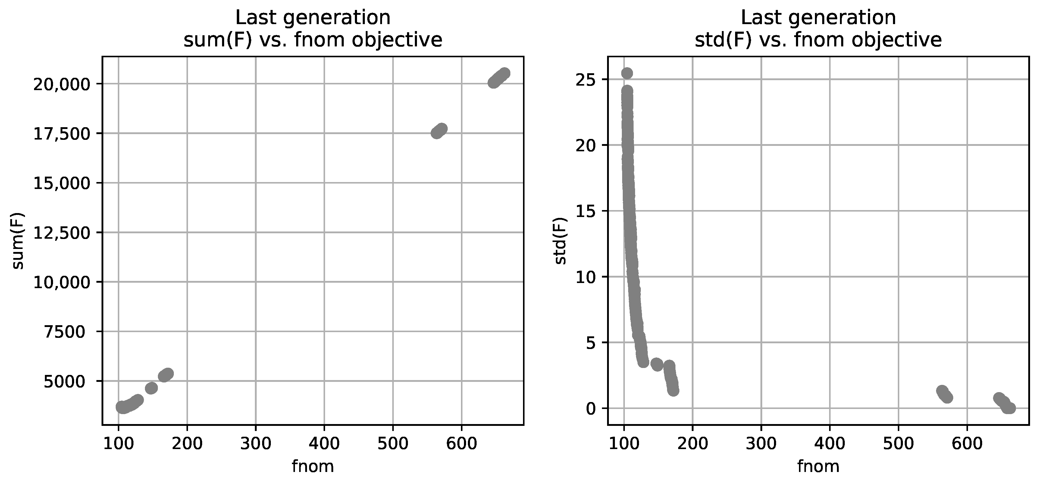
3.1. Square Root Circuit

The aim of the first experiment was to synthesize a square root computational circuit using a piecewise linear approximation. We let the synthesis algorithm search a space of every possible topology using 20 resistors (ranging from 10 to 10 4 Ω ), 12 rectifier diodes, and one voltage source (ranging from 0 to 6 V). The complete search parameters are listed in Table 2. After 2109 generations (95 h), running on a 10 × 4 Core i5 CPUs, we stopped the evolution manually. The values of the objectives f nom , F Σ , and σ F of the individual closest (in terms of Euclidean distance) to the coordinate origin were 9.30 , 2.250 × 10 3 , and 90.9 , respectively (see also Figure 6). Figure 7 shows the resulting circuit. Note that this is a raw circuit that needs to be equipped with SPICE simulator convergence helpers (i.e., 1 G Ω resistors between each node and the ground) before the actual simulation or optimization can be carried out. However, the convergence helpers are not drawn in the schematic. The voltage response of the circuit is shown in Figure 8, together with all the possible failure responses. Please refer to Section 3.4 for a more in-depth discussion of the results.

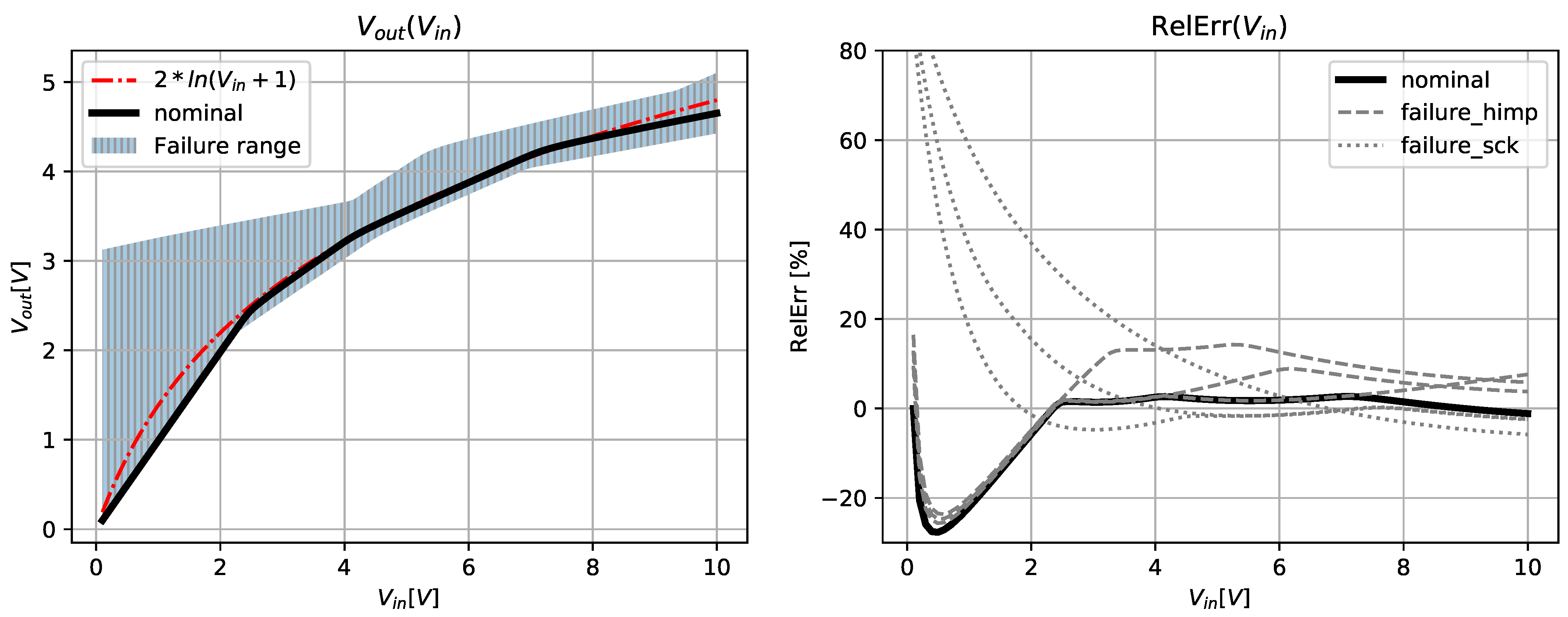
3.2. Natural Logarithm Circuit

Our second experiment was targeted to the exploration and synthesis of a circuit computing natural logarithm, specifically, the function g = 2 ln ( V in ) + 1 . We let the synthesis algorithm search the space of every possible topology using 20 resistors (ranging from 10 to 10 4 Ω ), 15 rectifier diodes, and two voltage sources (ranging from 0 to 6 V). The complete search parameters are listed in Table 3. After 2022 generations (43 h), we stopped the evolution manually. The values of the objectives f nom , F Σ , and σ F of the individual closest to the coordinate origin were 106, 3.62 × 10 3 , and 16.9 , respectively. Figure 9 shows the result space of the first Pareto front. The voltage response of the circuit is shown in Figure 10, together with all the possible failure responses.
In the evolution process, a natural logarithm computational circuit with a topology of 9 resistors and 11 diodes was produced (see Figure 11). Again, the convergence helpers are not drawn in the schematic. As seen in the figure, not all available components were included in the final solution, and the final topology consists of two separated branches. Please refer to Section 3.4 for a more in-depth discussion of the circuit.

3.3. Hardware Implementation

As the last of our three experiments, we conducted a hardware implementation of the square root computational circuit in Figure 7. The circuit was implemented on a bread board with discrete components (see Figure 12). The values of the resistors were chosen as the closest possible from the E12 or E24 series, and their production tolerance was between 5% and 10%. We used 1N4148 diodes.
Figure 13 shows the voltage responses obtained with real-world measurements. The circuit was excited (i.e., V i n ) using a 10 Hz sine wave from a laboratory signal generator, while V o u t was measured with a digital oscilloscope (points were saved for every possible component failure). Failures were implemented by either removing a diode (high-impedance failure) or short-circuiting it using a wire (short-circuit failure).

3.4. Discussion

The practical results of the presented research contribute to the synthesis of single-point failure-resilient electrical topologies. In the case of the square root computational circuit (Figure 8), we obtained a very close fit of the nominal circuit to the ideal square root function, with a constant offset of 0.2 V. This offset, however, can be compensated for using simple corrections of the circuit. Interestingly, stuck-open (i.e., high-impedance) failures produce a barely notable deviation from the nominal circuit response. The stuck-short (i.e., short-circuit) failures, however, are more severe since they cause noticeable anomalies in the circuit response. However, the computational error of a circuit that suffers such a failure is still manageable. Moreover, failure response curves are discernible (see, for example, the right chart in Figure 8), which can help engineers detect which particular device has failed. That may ease and speed up certain difficult diagnostic procedures. Future practitioners might consider adding error diversity as one of the objectives of their design.
Similar commentaries apply to the evolved failure-resilient natural logarithm computational circuit. In addition, we can see (Figure 10) that the nominal topology had a noticeable error in the range of 0 to 2 V of V i n , but fit well afterward. The computational error in the failure scenarios was slightly less scattered (and significantly less scattered in the range of 0 to 2 V) than in the case of a square root circuit. Surprisingly, high-impedance failures produced a larger response deviation than short-circuit failures in this case.
The observed significant error in the output characteristics of the natural logarithm circuit in the range of 0 to 2 V was due to the physical limitations of the passive circuit. Notice that the slope of the characteristics (from 0 to 2 V) is exactly 1 V/V. Theoretically, that is the steepest possible slope achievable in the DC domain for a passive linear circuit and hence is the best possible fit of the starting slope of the natural logarithm function. The evolutionary process was therefore able to find the best possible class of solutions using the given resources (i.e., component types and numerical parameters).
Figure 14 shows examples of hand-designed piece-wise linear square root and natural logarithm circuits. In order to make this topology robust to a single diode failure, we needed at least four diodes (i.e., a parallel connection of two pairs of diodes connected in series) in place of each of the three diodes in the circuit. Interestingly, the evolved square root (Figure 8) and natural logarithm circuits (Figure 11) had fewer diodes (i.e., 10 and 11, respectively). Since the inclusiveness requirement pushes the building blocks into the topology, we expected that all the available components (12 diodes in a square root and 15 diodes in a natural logarithm circuit, as shown in Table 2 and Table 3) to be included. We speculated that the evolution did not include all the components because the resulting performance outweighed the inclusiveness requirement in all of the objectives. Figure 15 and Figure 16 show the nominal and failure responses of conventionally designed nominal piece-wise computational circuits for square root and natural logarithm circuits respectively.
It is important to note that both topologies evolved in the experiments were the result of an artificial evolution with almost no human knowledge required in the synthesis part of the procedure. An exact problem statement and meticulous post-processing by an experienced designer are still needed to obtain the best results.
The results of the measurements using a hardware implementation confirmed the applicability of the concept, though there is a noticeable difference between the simulated and measured responses. However, the differences lie within the boundaries of resistor production tolerances (i.e., up to 10% performance drift of the nominal circuit version; see the relative error calculation in Figure 8 and Figure 13 for comparison). To the best of our knowledge, this is one of the rare evolutionary analog circuit syntheses (both robust and non-robust) confirmed in hardware.

4. Conclusions

Contemporary AI techniques are making exploring new circuit topologies less and less expensive. In this paper, we proposed new evaluation methods and used an evolutionary algorithm for the synthesis of analog circuit topologies with no single point of failure. Our experiments showed sucessful square root and natural logarithm circuit syntheses, which are robust to severe damage to rectifier diodes (both short- and open-circuit). We confirmed the applicability of the resulting square root circuit in hardware. Our approach does not require any expert knowledge to be input to the system. Rather, it relies on a well-defined fitness function. Further work might consider of failure combinations, which significantly increase the computational complexity of robustness calculation. Future researchers might also consider statistical possibilities for certain failure modes and include them into the robustness computation. We think that our work will inspire more research on the evolution of failure-resilient circuits. Our ongoing research, for example, is targeting evolving active failure-resilient circuits (i.e., with transistors).

Author Contributions

Conceptualization, Ž.R.; methodology, Á.B.; software, Ž.R. and Á.B.; validation, I.F.; formal analysis, Á.B.; investigation, I.F.; resources, Ž.R. and I.F.; data curation, Ž.R.; writing—original draft preparation, Ž.R.; writing—review and editing, I.F.; visualization, Ž.R.; supervision, Á.B.; project administration, I.F.; funding acquisition, Á.B. All authors have read and agreed to the published version of the manuscript.

Funding

The research was co-funded by the Ministry of Education, Science, and Sport (Ministrstvo za Šolstvo, Znanost in Šport) of the Republic of Slovenia through the program P2-0246 ICT4QoL—Information and Communications Technologies for Quality of Life.

Data Availability Statement

Data and program code are available at https://github.com/zigarojec/MatrixCircEvolutions (accessed on 26 November 2021).

Acknowledgments

Thanks to Brane Ždralo for technical support in circuit measurements.

Conflicts of Interest

The authors declare no conflict of interest.

Abbreviations

The following abbreviations are used in this manuscript:
AIArtificial intelligence
EAEvolutionary algorithm
GAGenetic algorithm
SASimulated annealing
MOEAMulti-objective evolutionary algorithm
PSOPfarticle swarm optimization
EHWEvolvable hardware
BJTBijunction transistor
VCOVoltage controlled oscillator
GPGenetic programming
GPGBGenetic programming + bond graphs
NNENeural network ensemble

References

  1. Gielen, G.G.; Rutenbar, R.A. Computer-Aided Design of Analog and Mixed-Signal Integrated Circuits. Proc. IEEE 2000, 88, 1825–1854. [Google Scholar] [CrossRef]
  2. MacLennan, B.J. Analog Computation. In Encyclopedia of Complexity and Systems Science; Meyers, R.A., Ed.; Springer: New York, NY, USA, 2009; pp. 271–294. [Google Scholar] [CrossRef]
  3. Burmen, Á.; Habal, H. Computing Worst-Case Performance and Yield of Analog Integrated Circuits by Means of Mesh Adaptive Direct Search. Inf. MIDEM 2015, 45, 160–170. [Google Scholar]
  4. Welchko, B.; Lipo, T.; Jahns, T.; Schulz, S. Fault Tolerant Three-Phase AC Motor Drive Topologies: A Comparison of Features, Cost, and Limitations. IEEE Trans. Power Electron. 2004, 19, 1108–1116. [Google Scholar] [CrossRef] [Green Version]
  5. Liu, M.; He, J. An Evolutionary Negative-Correlation Framework for Robust Analog-Circuit Design Under Uncertain Faults. IEEE Trans. Evol. Comput. 2013, 17, 640–665. [Google Scholar] [CrossRef]
  6. Kim, K.J.; Cho, S.B. Automated Synthesis of Multiple Analog Circuits Using Evolutionary Computation for Redundancy-Based Fault-Tolerance. Appl. Soft Comput. 2012, 12, 1309–1321. [Google Scholar] [CrossRef]
  7. Zebulum, R.; Vellasco, M.; Pacheco, M.; Sinohara, H. Evolvable Hardware: On the Automatic Synthesis of Analog Control Systems. In Proceedings of the 2000 IEEE Aerospace Conference. Proceedings (Cat. No.00TH8484), Big Sky, MT, USA, 25 March 2000; Volume 5, pp. 451–463. [Google Scholar] [CrossRef]
  8. Kim, K.J.; Cho, S.B. Combining Multiple Evolved Analog Circuits for Robust Evolvable Hardware. In Intelligent Data Engineering and Automated Learning—IDEAL 2009; Corchado, E., Yin, H., Eds.; Lecture Notes in Computer Science; Springer: Berlin/Heidelberg, Franch, 2009; pp. 359–367. [Google Scholar] [CrossRef]
  9. Hollinger, G.A.; Gwaltney, D.A. Evolutionary Design of Fault-Tolerant Analog Control for a Piezoelectric Pipe-Crawling Robot. In Proceedings of the 8th Annual Conference on Genetic and Evolutionary Computation, Seattle, NY, USA, 8 July 2006; GECCO ’06. Association for Computing Machinery: New York, NY, USA, 2006; pp. 761–768. [Google Scholar] [CrossRef] [Green Version]
  10. Ji, Q.; Wang, Y.; Xie, M.; Cui, J. Research on Fault-Tolerance of Analog Circuits Based on Evolvable Hardware. In Evolvable Systems: From Biology to Hardware; Kang, L., Liu, Y., Zeng, S., Eds.; Lecture Notes in Computer Science; Springer: Berlin/Heidelberg, Franch, 2007; pp. 100–108. [Google Scholar] [CrossRef]
  11. He, J.; Zou, K.; Liu, M. Section-Representation Scheme for Evolutionary Analog Filter Synthesis and Fault Tolerance Design. In Proceedings of the Third International Workshop on Advanced Computational Intelligence, Suzhou, China, 25–27 August 2010; pp. 265–270. [Google Scholar] [CrossRef]
  12. Kim, K.J.; Wong, A.; Lipson, H. Automated Synthesis of Resilient and Tamper-Evident Analog Circuits without a Single Point of Failure. Genet. Program. Evolvable Mach. 2010, 11, 35–59. [Google Scholar] [CrossRef]
  13. Hu, J.; Zhong, X.; Goodman, E.D. Open-Ended Robust Design of Analog Filters Using Genetic Programming. In Proceedings of the 7th Annual Conference on Genetic and Evolutionary Computation, Washington DC, USA, 25 June 2005; GECCO ‘05’. Association for Computing Machinery: New York, NY, USA, 2005; pp. 1619–1626. [Google Scholar] [CrossRef]
  14. Li, S.; Zou, W.; Hu, J. Novel Evolutionary Algorithm for Desi A gning Robust Analog Filters. Algorithms 2018, 11, 26. [Google Scholar] [CrossRef] [Green Version]
  15. Zebulum, R.S.; Stoica, A.; Keymeulen, D.; Sekanina, L.; Ramesham, R.; Guo, X. Evolvable Hardware System at Extreme Low Temperatures. In Proceedings of the International Conference on Evolvable Systems, Barcelona, Spain, 12–14 September 2005. [Google Scholar]
  16. Keymeulen, D.; Zebulum, R.S.; Jin, Y.; Stoica, A. Fault-Tolerant Evolvable Hardware Using Field-Programmable Transistor Arrays. IEEE Trans. Reliab. 2000, 49, 305–316. [Google Scholar] [CrossRef] [Green Version]
  17. Layzell, P.; Thompson, A. Understanding Inherent Qualities of Evolved Circuits: Evolutionary History as a Predictor of Fault Tolerance. In Evolvable Systems: From Biology to Hardware; Miller, J., Thompson, A., Thomson, P., Fogarty, T.C., Eds.; Lecture Notes in Computer Science; Springer: Berlin/Heidelberg, Franch, 2000; pp. 133–144. [Google Scholar] [CrossRef]
  18. Ando, S.; Iba, H. Analog Circuit Design with a Variable Length Chromosome. In Proceedings of the 2000 Congress on Evolutionary Computation. CEC00 (Cat. No.00TH8512), La Jolla, CA, USA, 16–19 July 2000; Volume 2, pp. 994–1001. [Google Scholar] [CrossRef] [Green Version]
  19. Hoover, R.C.; Roberts, R.G.; Maciejewski, A.A.; Naik, P.S.; Ben-Gharbia, K.M. Designing a Failure-Tolerant Workspace for Kinematically Redundant Robots. IEEE Trans. Autom. Sci. Eng. 2015, 12, 1421–1432. [Google Scholar] [CrossRef]
  20. Zhang, Y.; Jiang, J. Bibliographical Review on Reconfigurable Fault-Tolerant Control Systems. Annu. Rev. Control. 2008, 32, 229–252. [Google Scholar] [CrossRef]
  21. Wang, X.; Wang, S.; Yang, Z.; Zhang, C. Active Fault-Tolerant Control Strategy of Large Civil Aircraft under Elevator Failures. Chin. J. Aeronaut. 2015, 28, 1658–1666. [Google Scholar] [CrossRef] [Green Version]
  22. Zhang, W.; Xu, D.; Enjeti, P.N.; Li, H.; Hawke, J.T.; Krishnamoorthy, H.S. Survey on Fault-Tolerant Techniques for Power Electronic Converters. IEEE Trans. Power Electron. 2014, 29, 6319–6331. [Google Scholar] [CrossRef]
  23. Mirhoseini, A.; Goldie, A.; Yazgan, M.; Jiang, J.W.; Songhori, E.; Wang, S.; Lee, Y.J.; Johnson, E.; Pathak, O.; Nazi, A.; et al. A Graph Placement Methodology for Fast Chip Design. Nature 2021, 594, 207. [Google Scholar] [CrossRef] [PubMed]
  24. Kruiskamp, W.; Leenaerts, D. Darwin: Analogue Circuit Synthesis Based on Genetic Algorithms. Int. J. Circuit Theory Appl. 1995, 23, 285–296. [Google Scholar] [CrossRef]
  25. Koza, J.R. Genetic Programming: On the Programming of Computers by Means of Natural Selection; MIT Press: Cambridge, MA, USA, 1992. [Google Scholar]
  26. Koh, H.Y.; Sequin, C.H.; Gray, P.R. OPASYN: A Compiler for CMOS Operational Amplifiers. IEEE Trans. -Comput.-Aided Des. Integr. Circuits Syst. 1990, 9, 113–125. [Google Scholar] [CrossRef]
  27. McConaghy, T.; Palmers, P.; Steyaert, M.; Gielen, G.G.E. Trustworthy Genetic Programming-Based Synthesis of Analog Circuit Topologies Using Hierarchical Domain-Specific Building Blocks. IEEE Trans. Evol. Comput. 2011, 15, 557–570. [Google Scholar] [CrossRef]
  28. Sorkhabi, S.E.; Zhang, L. Automated Topology Synthesis of Analog and RF Integrated Circuits: A Survey. Integration 2017, 56, 128–138. [Google Scholar] [CrossRef]
  29. Baumann, R. Radiation-Induced Soft Errors in Advanced Semiconductor Technologies. IEEE Trans. Device Mater. Reliab. 2005, 5, 305–316. [Google Scholar] [CrossRef]
  30. Schwank, J.R.; Shaneyfelt, M.R.; Fleetwood, D.M.; Felix, J.A.; Dodd, P.E.; Paillet, P.; Ferlet-Cavrois, V. Radiation Effects in MOS Oxides. IEEE Trans. Nucl. Sci. 2008, 55, 1833–1853. [Google Scholar] [CrossRef]
  31. Dong, H.; Wang, M.; Luo, Y.; Zheng, M.; An, M.; Ha, Y.; Pan, H. PLAC: Piecewise Linear Approximation Computation for All Nonlinear Unary Functions. IEEE Trans. Very Large Scale Integr. (VLSI) Syst. 2020, 28, 2014–2027. [Google Scholar] [CrossRef]
  32. Rojec, Ž.; Burmen, Á.; Fajfar, I. Analog Circuit Topology Synthesis by Means of Evolutionary Computation. Eng. Appl. Artif. Intell. 2019, 80, 48–65. [Google Scholar] [CrossRef]
  33. Rojec, Ž.; Olenšek, J.; Fajfar, I. Analog Circuit Topology Representation for Automated Synthesis and Optimization. Inf.-Midem-J. Microelectron. Electron. Components Mater. 2018, 48, 29–40. [Google Scholar]
  34. Tomasz, D.G. Genetic Algorithms Reference; TOMASZGWIAZDA E-BOOKS: Łomianki, Poland, 2006. [Google Scholar]
  35. Olenšek, J.; Tuma, T.; Puhan, J.; Burmen, Á. A New Asynchronous Parallel Global Optimization Method Based on Simulated Annealing and Differential Evolution. Appl. Soft Comput. 2011, 11, 1481–1489. [Google Scholar] [CrossRef]
  36. Deb, K.; Pratap, A.; Agarwal, S.; Meyarivan, T. A Fast and Elitist Multiobjective Genetic Algorithm: NSGA-II. Trans. Evol. Comp 2002, 6, 182–197. [Google Scholar] [CrossRef] [Green Version]
  37. Băjenescu, T.I.; Bâzu, M.I. Reliability of Diodes. In Reliability of Electronic Components: A Practical Guide to Electronic Systems Manufacturing; Băjenescu, T.I., Bâzu, M.I., Eds.; Springer: Berlin/Heidelberg, Franch, 1999; pp. 145–170. [Google Scholar] [CrossRef]
  38. PyOPUS—Simulation, Optimization, and Design; EDA Laboratory, Faculty of Electrical Engineering, University of Ljubljana: Ljubljana, Slovenia, 2017. Available online: http://spiceopus.si/pyopus/quickstart.html (accessed on 3 June 2021).
  39. Kenneth, A.K. Piecewise Linear Circuits, Analog Integrated Electronics EE431/EE531, Practical Manual; University of Alabama at Birmingham: Birmingham, Alabama, 2004. [Google Scholar]
Figure 1. An example of an analog circuit topology represented by an upper-triangular incident matrix. Every logical one connects two terminals of listed components or outer terminals [33].
Mathematics 10 00156 g001
Figure 2. Topology crossover. In offspring 1, only the node location of one device terminal is exchanged. In offspring 2, three node locations are exchanged. For better illustration, the right parent is a full upper-triangular matrix [32].
Mathematics 10 00156 g002
Figure 3. Rectifier false-robustness problem.
Mathematics 10 00156 g003
Figure 4. The flowchart of the evolutionary algorithm. Every tenth generation, a full parameter optimization is triggered on best individuals.
Mathematics 10 00156 g004
Figure 5. Rectifier diode failure modeling. (Left) The nominal model with inclusiveness measurement voltmeter. (Center) A high-impedance diode failure. (Right) A short-circuit diode failure.
Mathematics 10 00156 g005
Figure 6. The Pareto front of the last generation of the evolution of the failure-resilient square root circuit. Shown are the tree objectives f nom , F Σ , and σ F .
Mathematics 10 00156 g006
Figure 7. The evolved topology of failure-tolerant square root circuit (raw evolution result).
Mathematics 10 00156 g007
Figure 8. The voltage response of the resulting failure-resilient square root circuit. (Left):The complete output range, where the red (dash-dot) curve represents the ideal square root function, the black (solid) curve represents the failure-free circuit, and the gray area represents the range of responses with all possible single diode failures. (Right) Relative deviations from the ideal square root function ( R e l E r r ( V i n ) = V o u t V i n max ( V o u t , V i n ) ) . A nominal design offset is subtracted from V o u t for R e l E r r ( V i n ) representation. Stuck-open failures are drawn in dashed lines while stuck-short failures are drawn in dotted lines.
Mathematics 10 00156 g008
Figure 9. The Pareto front of the last generation of the evolution of the failure-resilient natural logarithm circuit. Shown are the tree objectives f nom , F Σ , and σ F .
Mathematics 10 00156 g009
Figure 10. The voltage response of the resulting failure-resilient natural logarithm circuit. (Left) The complete output range, where the red (dash-dot) curve represents the ideal natural logarithm function, the black (solid) curve represents the failure-free circuit, and the gray area represents the range of responses with all possible single diode failures. (Right) Relative deviations from the ideal natural logarithm function ( R e l E r r ( V i n ) = V o u t 2 ln ( V i n + 1 ) max ( V o u t , 2 ln ( V i n + 1 ) ) ) . Stuck-open failures are drawn in dashed lines while stuck-short failures are drawn in dotted lines.
Mathematics 10 00156 g010
Figure 11. The evolved topology of a failure-tolerant natural logarithm circuit (raw evolution result).
Mathematics 10 00156 g011
Figure 12. A bread-board implementation of a failure-resilient square root circuit.
Mathematics 10 00156 g012
Figure 13. The measured voltage response of a real-world prototype failure-resilient square root circuit. (Left) The complete output range where the red (dash-dot) curve represents the ideal square root function, the black (solid) curve represents the failure-free circuit, and the gray area represents the range of responses with all possible single diode failures. (Right) Relative deviations from the ideal square root function ( R e l E r r ( V i n ) = V o u t V i n max ( V o u t , V i n ) ) . A nominal design offset is subtracted from V o u t for R e l E r r ( V i n ) representation. Stuck-open failures are drawn in dashed lines while stuck-short failures are drawn in dotted lines.
Mathematics 10 00156 g013
Figure 14. Examples of hand-designed piece-wise linear computational circuits: (Left) square root and (Right) natural logarithm [39].
Mathematics 10 00156 g014
Figure 15. The simulated voltage response of an example of a hand-designed piece-wise linear square root circuit. (Left) The complete output range where the red (dash-dot) curve represents the ideal square root function, the black (solid) curve represents the failure-free circuit, and the gray area represents the range of responses with all possible single diode failures. (Right) Relative deviations from the ideal square root function ( R e l E r r ( V i n ) = V o u t V i n max ( V o u t , V i n ) ) . A nominal design offset is subtracted from V o u t for R e l E r r ( V i n ) representation. Stuck-open failures are drawn in dashed lines while stuck-short failures are drawn in dotted lines.
Mathematics 10 00156 g015
Figure 16. The simulated voltage response of an example of a hand-designed piece-wise linear the natural logarithm circuit. (Left) The complete output range where the red (dash-dot) curve represents the ideal natural logarithm function, the black (solid) curve represents the failure-free circuit, and the gray area represents the range of responses with all possible single diode failures. (Right) Relative deviations from the ideal natural logarithm function ( R e l E r r ( V i n ) = V o u t 2 ln ( V i n + 1 ) max ( V o u t , 2 ln ( V i n + 1 ) ) ) . Stuck-open failures are drawn in dashed lines while stuck-short failures are drawn in dotted lines.
Mathematics 10 00156 g016
Table 1. Previous work on the evolutionary synthesis of analog circuits for robust design and fault tolerance.
AuthorsMethodGoalsFailure ToleranceHW
Verification
Zebulum et al. [7]EACompensator circuitBJT removal/
Kim and Cho [8]EALow-pass filterR/L/C removal/
Hollinger and Gwaltney [9]GAPID controllerR/L/C removal
actuator failure
Yes
Ji et al. [10]GA+SAAmplifierTransistor failure/
He et al. [11]EALow-pass filterParameter drift/
Kim et al. [12]Co-EALow-pass filterR/L/C partial
short/disconnect
Yes
Hu et al. [13]GPBGPassive filtersR/L/C parameter perturbation/
Li et al. [14]GPPassive filtersParameter perturbation/
Zebulum et al. [15]In-situ EAHalf-wave rectifier,
NOR gate, VCO
Extreme-low temperaturesYes
Keymeulen et al. [16]In-situ GAXNOR gate,
analog multipler
Arbitrary faults in FPTAYes
Layzell and Thompson [17]GAInverter
amplifier
oscillator
BJT removalYes
Ando and Iba [18]EAPassive filtersR/L/C parameter perturbation/
Liu and He [5]ENCFPassive filtersOne/multi-component
(full/partial)
short/disconnection
and combinations
/
Kim and Cho [6]Multi-pop. EAPassive filtersOne R/L/C removal/
This workNSGA-IIComputational circuitsSemiconductor diode failure
open- and short-circuit
Yes
Table 2. The search parameters of the evolution of a failure-resilient square root analog circuit.
Resistors avail.20
Voltage sources avail.1
Diodes avail.12
Population size400
Tournament size3
Mating prob.0.6
Topology change prob.0.7
PSADE enabledEvery 10th gen.
Table 3. The search parameters of the evolution of a failure-resilient natural logarithm analog circuit.
Resistors avail.15
Voltage sources avail.1
Diodes avail.15
Population size400
Tournament size3
Mating prob.0.4
Topology change prob.0.5
PSADE enabledEvery 10th gen.
Publisher’s Note: MDPI stays neutral with regard to jurisdictional claims in published maps and institutional affiliations.

