1. Introduction
Generally speaking, real-time image processing on a serial processor is very difficult to achieve, mainly due to the large dataset represented by the image or the complex operations that may need to be performed [
1]. A hardware-based solution is much more preferable for our implementation as the parallelization benefits are huge, comparing to other platforms. Image processing involves a massive amount of pixel operations, which can be parallelized on hardware due to the repetitive nature of the algorithms applied; therefore, the use of a field-programmable gate array (FPGA) is a good alternative [
2]. FPGAs have become popular as implementation platforms, mainly due to their continual growth in functionality and size, especially for image processing applications and video processing [
3]. A first step for many digital image processing applications and computer vision is the edge detection. Edge detection in general can reduce significantly the amount of data in an image, while the structural properties of the image are preserved, in order to be used for further image processing [
4], reducing the processing complexity and facilitating the implementation of the main algorithm [
5]. Although edge detection is a valuable step in image processing, it is very taxing in hardware and power requirements; thus, the need for a dedicated accelerator is inevitable. In our previous research, we published a “bare-metal” VHDL design as a portable USB accelerator [
6]. In this paper, we are using a different workflow, utilizing modern software for a similar implementation based on High-Level Synthesis (HLS).
High-level synthesis (HLS) is most commonly used when designing both high-performance and energy-efficient heterogeneous systems, by addressing the complexity of today’s systems, as well as shortening time-to-market [
7]. HLS, a vivid research domain, allows designers to use a software program for hardware functionality specification, while working in a higher level of abstraction. Additionally, HLS is quite an interesting approach in cases of field-programmable gate array circuits designs, where hardware implementations can be easily replaced and refined in the target device [
8]. In recent years, the use of HLS has greatly increased, while offering many academic as well as industrial tools. These tools use different types of input languages, produce results of different quality, even for the very same input description, and perform different internal optimizations. Thus, it is very challenging to compare their performance and find the best-suited implementation for the current constraints [
9].
To be able to compare the two different workflows (pure HDL and HLS), we implemented a grayscale and an edge detection module in both designs, based on the Sobel operator algorithm, to produce an output image containing only the edges of the input. The rest of the paper is structured as follows. In the following section, we present a list of similar research done, related to our implementation. Then, we describe the hardware architecture of our previous VHDL design, the software and bitstream configuration required, and a detailed analysis of our image processing modules. We do the same for the new HLS implementation and, finally, we present the results of our work.
2. Related Work
In this section, we present state-of-the-art related research work. An interesting research was presented by Knittel, named a PCI-compatible FPGA-coprocessor for 2D/3D image processing [
10]. An FPGA board for PCI systems is presented that features one XC3195A FPGA (<9 K gate equivalents), three XC4013 devices (each up to 13 K gate equivalents), 2 MByte of Flash Memory, 256 KByte of high-speed SRAM and a 16-bit high-speed multiply and accumulate unit. The design is used for scientific visualization to speed up algorithms and 3D-datasets. Due tomany bit and short integer operations, the calculations can be efficiently offloaded to the FPGA. This is a research that can be used as a starting point for speech or image processing, as well. While the transfer bandwidth is high because of the intensive computations, this is not an issue on the PCI bus. In contrast to our research, the accelerator is PCI-based, which is considered as a heavy workstation modification and does not meet the portability criteria.
An early published research was a computational analysis to edge detection [
11] by Canny. The author defined detection and localization criteria for a class of edges, and presented mathematical forms for these criteria as functionals on the operator impulse response. A third criterion is then added to ensure that the detector has only one response to a single edge. He used the criteria in numerical optimization to derive detectors for several common image features, including step edges. On specializing the analysis to step edges, there is a natural uncertainty principle between detection and localization performance, which are the two main goals. With this principle, he derived a single operator shape that is optimal at any scale. The optimal detector has a simple approximate implementation, in which edges are marked at maxima in gradient magnitude of a Gaussian-smoothed image. He extended this simple detector using operators of several widths to cope with different signal-to-noise ratios in the image. He presented a general method, called feature synthesis, for the fine-to-coarse integration of information from operators at different scales. Finally, the author showed that step edge detector performance improves considerably as the operator point spread function is extended along the edge. Although this research is obsolete and the author focused on the computational part without carrying out any implementation, it has inspired many researchers as a starting point for their work.
Lastly, we mention the Multi-Resolution FPGA-Based Architecture for Real-Time Edge and Corner Detection [
12]. This research presents a parameterizable architecture for both image and video processing. It features low latency and memory requirements and supports variable input resolution. The architecture is optimized for feature detection using the Canny edge detector and the Harris corner detector. It contains neighborhood extractors and threshold operators that can be parameterized at runtime. In addition, algorithm simplifications are employed, to reduce mathematical complexity, memory requirements, and latency without losing reliability. Although this is an interesting research, the authors compared their work to a graphics processing unit (GPU), and not an HLS-based FPGA design.
3. The “Bare-Metal” VHDL Design Implementation
In our previous research, we presented a design implementation of the Grayscale and Edge Detection modules. The design was written purely in VHDL, simulated in Altera’s Quartus 15.0 and synthesized on a DE2-115 Cyclone IV E. The Altera Cyclone® IV EP4CE115 FPGA device equipped on the DE2-115 features 114,480 logic elements (LEs), up to 3.9-Mbits of RAM, and 266 multipliers. The board also features a USB Host/Slave Controller from Cypress (CY7C67200) with USB type A and type B connectors.
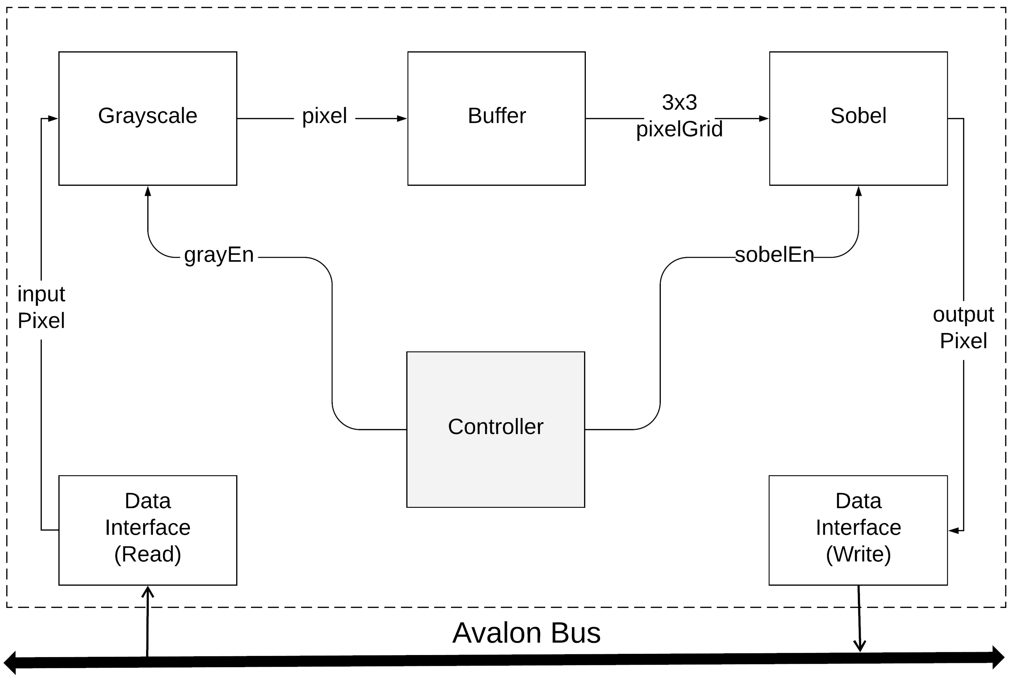
3.1. Image Processing Cores
Our design contains two processing modules, Grayscale and Sobel edge detection (
Figure 1). The latter utilizes the output of the grayscale as input, demonstrating chaining of different modules, in order to achieve different filter effects in a future expansion.
3.1.1. Grayscale
The original color image is converted into a grayscale image using the original ITU-R recommendation (BT.709, specifically), which is the historical precedent. The coefficients, shown in Equation (
1), are used to convert a pixel to gray. The
R,
G, and
B symbols correspond to the channel name (Red, Green, and Blue, respectively), and
contains the final pixel value.
3.1.2. Edge Detection
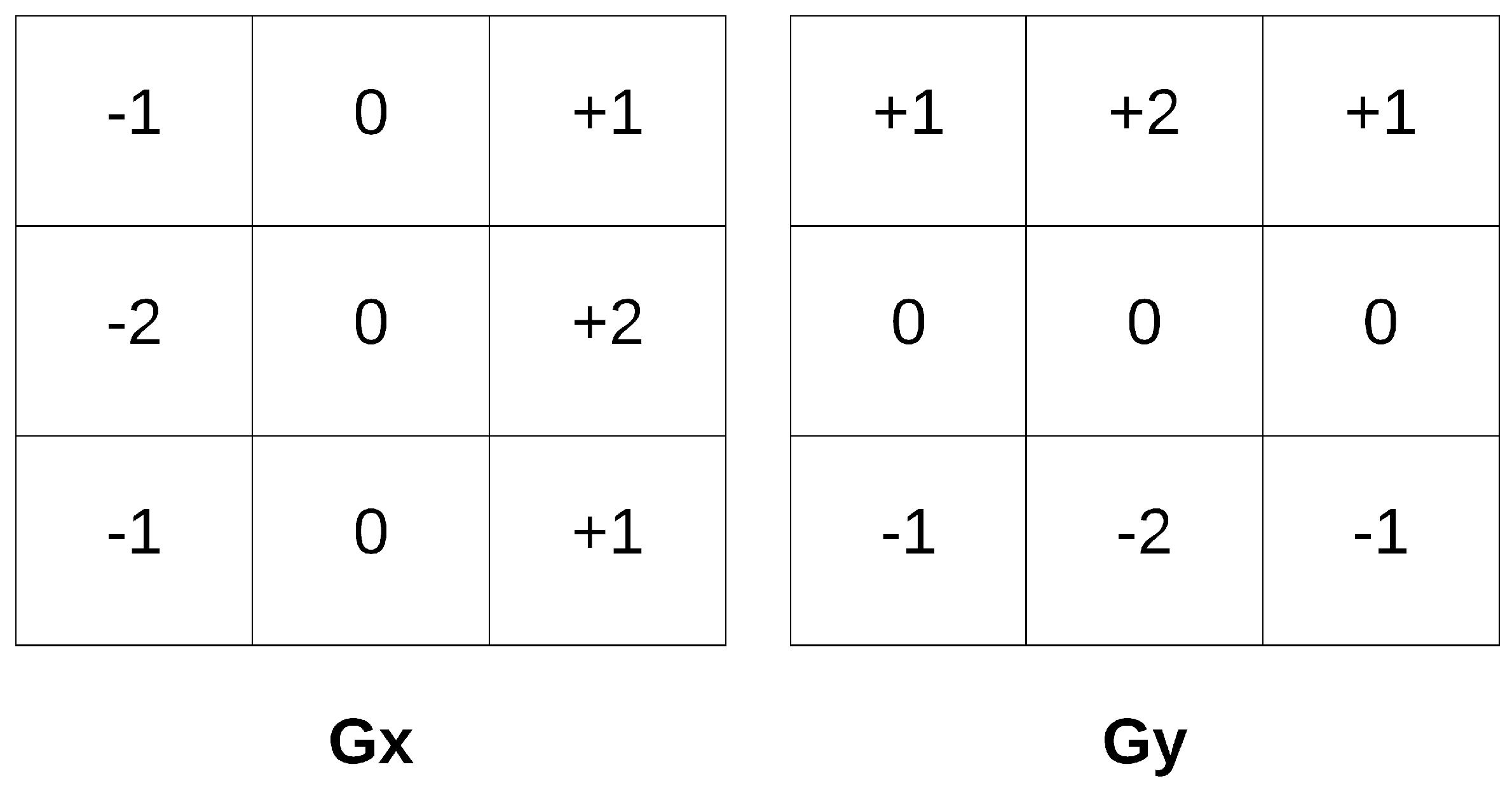
We utilized separate horizontal and vertical gradient detection kernels in the algorithm of the Sobel Edge Detector. The calculation of
and
is performed using the Sobel Operator. It uses a pair of 3 × 3 convolution masks (
Figure 2); the first one estimates the gradient in the x (columns) and the other one the gradient in the y-direction (rows). If the pixel’s gradient direction is one of the eight possible main directions, the gradient magnitude of this pixel is compared with two of its immediate neighbors along the gradient direction. The gradient magnitude is set to zero, if it does not correspond to a local maximum of
gradients. The pixel without local maximum gradient magnitude is removed as the direction of the gradient is known. The approximate absolute gradient magnitude (edge strength) at each point is computed by Equation (
2).
By using the aforementioned approximation formula, the calculation is simplified, leading to a reduced number of operations needed, since there is no need for square roots and trigonometric lookup tables to be invoked.
3.2. FPGA Bitstream
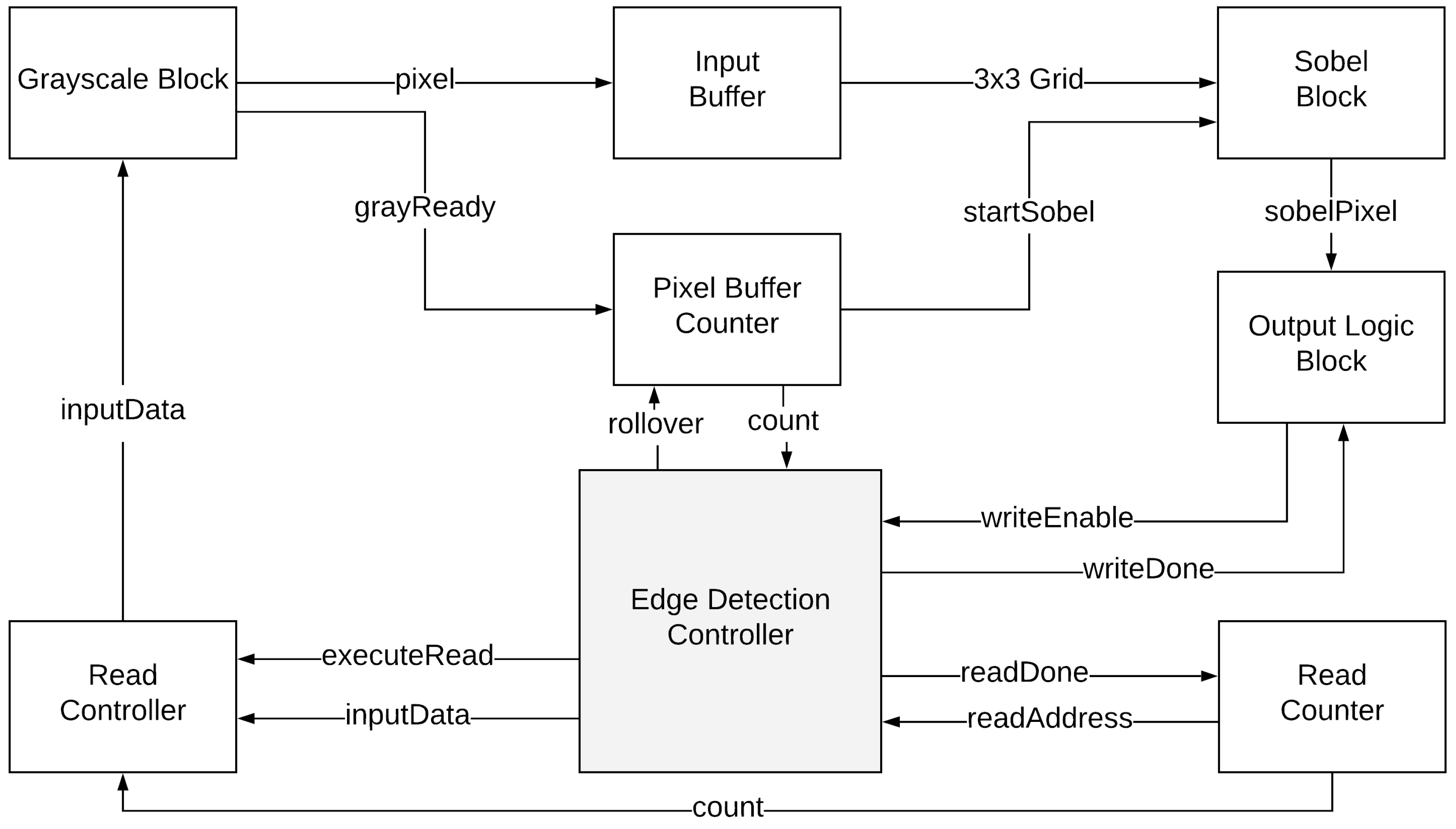
A NIOS soft CPU implementation decodes the transferred packet, identifying it by a special type of word in the packet (RX_TYPE) with HPI read. The program asserts a start process byte (0 × 53) to a predetermined Control Status Register (CSR) to signal the Avalon VHDL interface to move forward with the actual execution of the image detection algorithm. Then, it waits for the stop byte (0 × 12) from the custom interface to stop the execution. The CPU remains in the idle state until a start signal is asserted. Once it is asserted, the readEnable signal is asserted to allow the FPGA to read the 24-bit signal.
After a readDone signal is asserted, the CPU waits until the pixel is grayed. Once it is grayed, a state that controls storing the grayed pixel in a buffer is triggered. This state also waits until the buffer has enough pixels for applying the Sobel algorithm. Furthermore, the writeEnable signal is asserted and the CPU waits for the writeDone signal; then, the process restarts by retrieving a new packet. There is also an error flag, in the case anything goes wrong with reading or writing. The design flow is depicted in
Figure 3.
The entire design synthesizes completely, without any inferred latches, timing arcs, and sensitivity list warnings. Source and mapped version of the complete design behave the same for all of our test cases. The mapped version simulates without timing errors, apart from time zero. The maximum number of clock cycles processing a single pixel value is 16. The timing analysis of the design is described in
Table 1 and
Table 2, and the fitter resource utilization in
Table 3.
3.3. Firmware
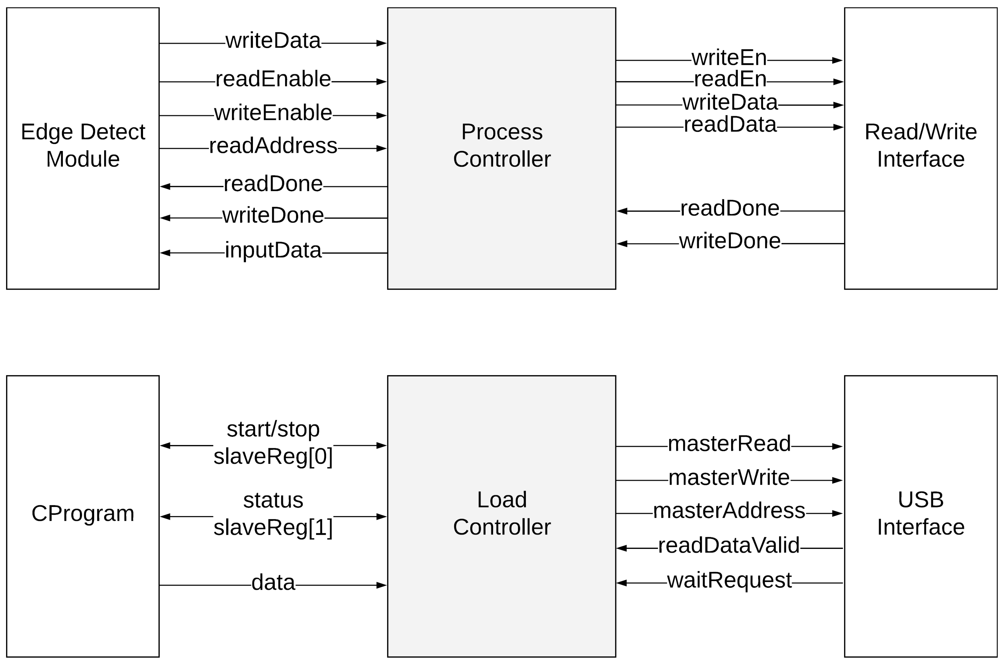
A NIOS II soft processor was used to implement the USB protocol. NIOS CPU drives the CY7C67200 USB interface, encoding/decoding packets with the host. The CPU is also connected to the image processing peripherals via the Avalon MM interface. The VHDL interface (custom master-slave) receives the 24-bit pixel and the start byte from the CPU and then moves to a STARTPROCESS state. The module asserts the finish conversion flag, to signal the CPU that the image data are valid and ready to be transferred to the host. The custom edge detection block, written in VHDL, interacts with the NIOS on-chip memory using the READ and WRITE interfaces. The execution of the block is described in
Figure 4. During execution, the edge detection block retrieves the values of 9 pixels from the memory and processes them to produce the final pixel value of the edge detected image. This pixel is written down serially (as we perform a raster scan) into the memory location. After the pixel is processed, the custom master–slave program moves to WRITESTOPBYTE state to assert a stop signal, which signals the C program to terminate execution. At this point, the line detected version of the image is displayed on the PC application.
3.4. Host Software
Altera’s DE2-115 USB Controller; CY7C67200 and the host application implemented in C programming language are parts of the software on the workstation. We implemented an application to utilize the communication facility. Our application accepts as input a Bitmap (BMP) image file, which is then transferred to FPGA, and presents the resulting processed image. The BMP file format can store two-dimensional images (both monochromatic and colored), in different color depths, optionally with data compression, alpha channels, and color profiles. For our implementation, 24-bit Bitmap images without compression (BI_RGB None) are used. The specifications can be easily extended as the decoding of the image is separated from the main design. Each image pixel is decoded into the 24-bit RGB channels representing 0–255 different values (True Color). Immediately after, a packet composed of the corresponding prefix (RX_TYPE) and the 24-bit channels is then sent to the USB endpoint.
At this point, the description of the VHDL implementation is finished. We conclude that an accelerator implementation in pure VHDL can be quite a time-consuming process, especially in cases where the developer starts from scratch, without using any predefined templates.
4. The HLS Design Implementation
For our HLS implementation, we used a Pynq-Z1 board from Xilinx. This board is designed to be used with PYNQ, an open-source framework that enables embedded programmers to exploit the capabilities of Xilinx Zynq All Programmable SoCs (APSoCs) without having to design programmable logic circuits. Instead, the APSoC is programmed using Python and the code is developed and tested directly on the PYNQ-Z1. The programmable logic circuits are imported as hardware libraries and programmed through their APIs in essentially the same way that the software libraries are imported and programmed. The board is based on ZYNQ XC7Z020-1CLG400C and includes a 650 MHz dual-core Cortex-A9 processor, 13.300 logic slices, each with four 6-input LUTs and 630 KB of fast block RAM. In addition, it includes 220 DSP slices and 512 MB DDR3 with 16-bit bus @ 1050 Mbps. This board also features HLS support, in contrast to the previous used Altera DE2-115, which does not provide a similar pipeline.
The design was implemented in a more modern approach. The Vivado HLS software [
13] was used to produce VHDL from C++ code to create the HDL description. Apart from the main HDL blocks, some other blocks were assembled and configured accordingly, in order to use them as a Python overlay on a Pynq-Z1 board from Xilinx.
4.1. Image Processing Core
In the second design, we exploited HLS capabilities to generate the Intellectual Property (IP) cores, by using C++ code written by us. In the new design, we combined the Grayscale and Edge Detection modules together, to further reduce the resource utilization. To exploit parallelism at these levels, we needed each application’s timing diagrams for various inputs and function calls, as well as an in-depth code analysis. In this paper, our goal is each function’s optimization by exploiting a variety of design techniques, namely loop unrolling and pipelining.
4.1.1. Edge Detection
The HLS implementation for the Edge Detection IP consists of four stages. The first (AXIS2GrayArray) and the last (GrayArray2AXIS) are responsible for transferring the image data through the AMBA AXI4-Stream Protocol Specification. We combine the grayscale conversion into the first stage to simplify the design. In the second stage, we applied the Sobel operator but, to improve the edge detection and provide more accurate results, we applied a Non-Max suppression algorithm, which helps to eliminate the points that do not lie in important edges [
14].
4.1.2. Int2RGB
The second IP helps to improve image reconstruction performance by offloading CPU calculations to Programmable Logic (PL), as the three RGB channels are encoded into a 32-bit unsigned integer (Listing 1). This is a crucial step, because, as we discovered in our experiments, performing this computation on the CPU incurred 70 s extra delay for every image of 640 × 480 pixels. Using our optimization, we reduced this operation to under 1 s. We implemented it through AXI4-Stream, further optimizing the transfer of the data by using a bidirectional DMA (read and write), benefiting our architecture with reduced resource usage, in contrast to other implementations, which use one DMA for reading and one for writing.
| Listing 1. The formula that decodes an unsigned integer to three RGB channels. |
//Channel:
|
//1 - Red, 2 - Blue , 3 - Green
|
out_data->data = (in_data->data & 0xff0000) >> 16;
|
out_data->data = (in_data->data & 0x00ff00) >> 8;
|
out_data->data = in_data->data & 0x0000ff;
|
4.2. FPGA Bitstream
Pynq-Z1 is a Zynq-7000 ARM/FPGA System on Chip (SoC), which utilizes the AMBA [
15] architecture; therefore, for the communication, we used AXI [
16], an interface standard that allows communication of different components with each other. An AXI link consists of the AXI master, capable of initiating transactions, and the AXI slave, which responds to the master’s initiated transactions [
17]. One approach is the use of one of two types of AXI interfaces, AXI stream interface and AXI mapped interface. Specifically, AXI4 allows a burst of up to 256 data transfer cycles with just a single address phase and, therefore, is used for memory mapped interfaces. In addition, AXI4-Stream allows an unlimited size of burst data and removes the memory address phase requirement altogether; however, due to their lack of address phases, AXI4-Stream interfaces and transfers are not considered to be memory-mapped [
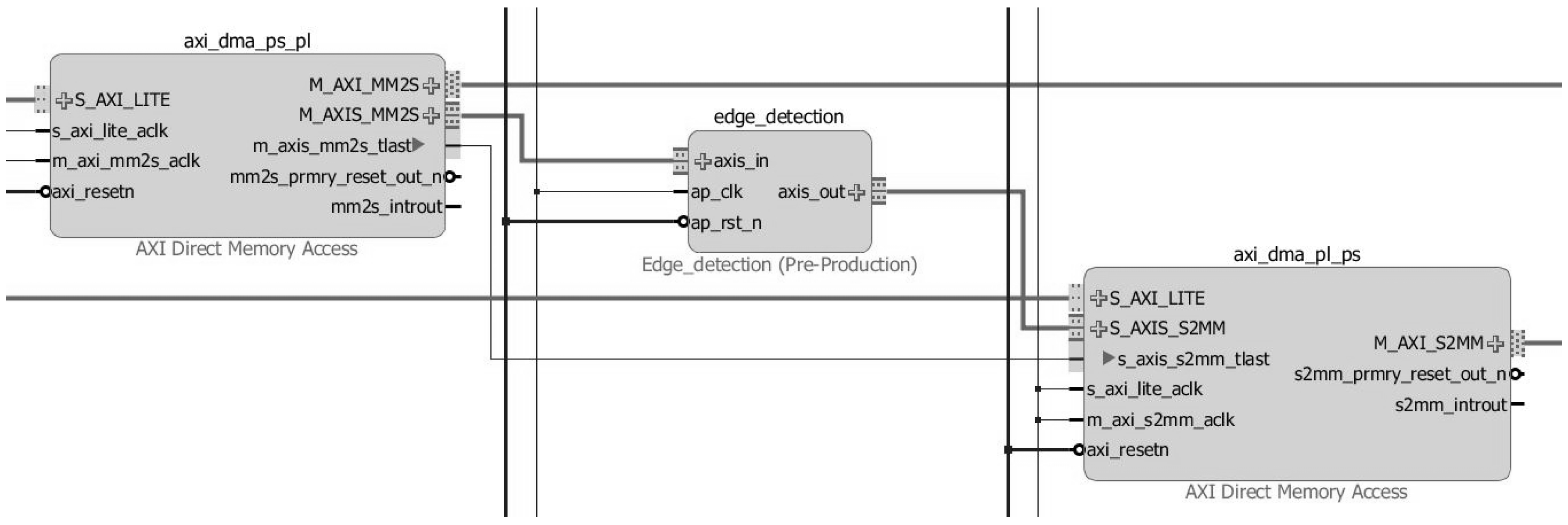
18]. Another approach would be the construction of systems that lead to the combination of AXI memory mapped IP and enhance it with AXI4-Stream. To move streams in and out of the shared memory, a DMA engine can be used. For this reason, we used AXI Direct Memory Access (DMA) IPs (
Figure 5), which provide a direct memory access of a high bandwidth between the AXI4-Stream IP and AXI4 memory mapped interfaces [
19].
Figure 5 depicts a block diagram with the interface connections of the Edge Detection with the DMA input and output of data. Researchers have reported that, at a clock frequency of 100 MHz, data transitions may be established from both AXI4 master and AXI-Stream slave to AXI4 master at a data rate of 400 MBps and 300 MBps, respectively, being a quota of the theoretical bandwidths of 99.76% and 74.64%. These numbers were used to help us find the overhead of the data transfer between the Zynq device’s Processing System (PS) and PL [
20].
Table 4 indicates the timing summary as reported by Vivado 2016 with the Pynq-Z1 project for our complete system implementation.
Table 5 summarizes the hardware utilization for the overall system we implemented in this study. The table reports the number of logical elements and memory bits needed to implement the functions presented above, in a small FPGA chip, the Pynq-Z1 (Zynq-7000) [
21]. We should mention the low utilization percentage of available LUT memory bits.
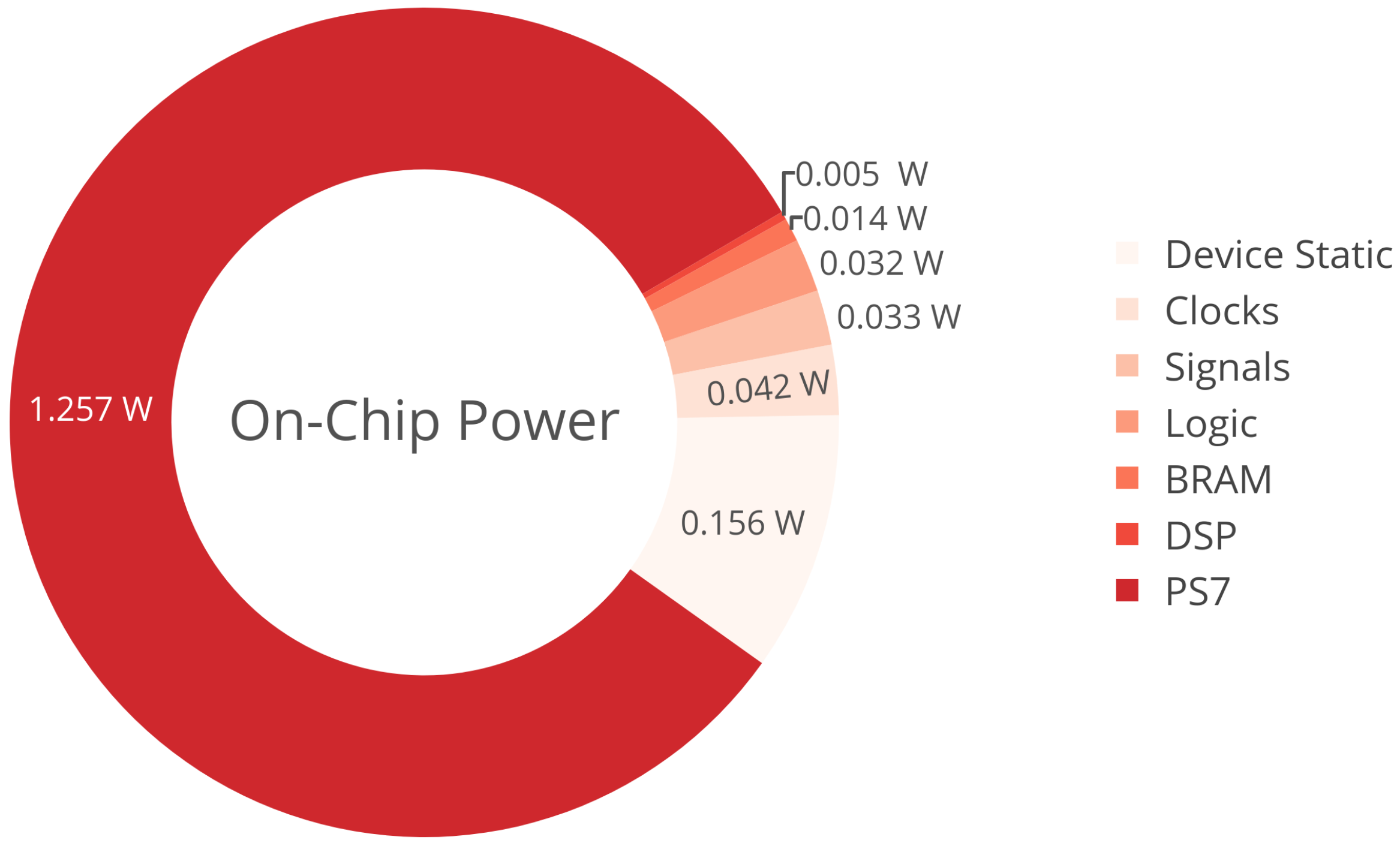
Figure 6 indicates the power consumption of our implementation, as reported by Vivado after synthesis. The static power consumption is around 0.156 watt (10%) of the total dynamic power requirements (1.383 watts). We can safely assume that, with the Zynq processing system (PS7) idle, we can expect an average power consumption of 0.5 watt and below. In comparison with other accelerators, such as that in [
10], which often exceed 1.5 watts of power consumption, our implementation is about three times more energy efficient.
4.3. Firmware
We used the Python libraries provided with the base image of Pynq-Z1 for the firmware. We downloaded the overlay on the board and we initialized the DMAs for interaction. Then, we streamed the input buffer to the PSPL DMA, waited for the DMAs to assert the finish signal and read the output buffer from the PLPS DMA.
5. Experimental Measurements
To assess both our designs, we performed a number of experiments. Our input set consisted of 50 images of 640 × 480 BMP uncompressed format. Our boards were connected to our workstation via USB 2.0 interface (DE2-115) and Ethernet 100 Mbps (Pynq-Z1). The workstation consists of an Intel Core i5-4460 CPU @ 3.20 GHz and 16 gigabytes of RAM running Microsoft Windows 10 operating system.
We compared the results using the peak signal-to-noise (
) ratio [
22]. This ratio is often used as a quality measurement between the original and a compressed image. The higher is the
, the better is the quality of the compressed or reconstructed image. The Mean Square Error (
) and the Peak Signal to Noise Ratio (
) are the two error metrics used to compare image compression quality. The
represents the cumulative squared error between the compressed and the original image, whereas
represents a measure of the peak error. The lower is the value of
, the lower is the error.
In Equation (
3),
M and
N are the number of rows and columns in the input images, respectively. For the PSNR calculation (Equation (
4)),
R is the maximum fluctuation in the input image data type. For example, if the input image has a double-precision floating-point data type, then
R is 1. For our comparison, we used an 8-bit unsigned integer data type, thus
R equals to 255.
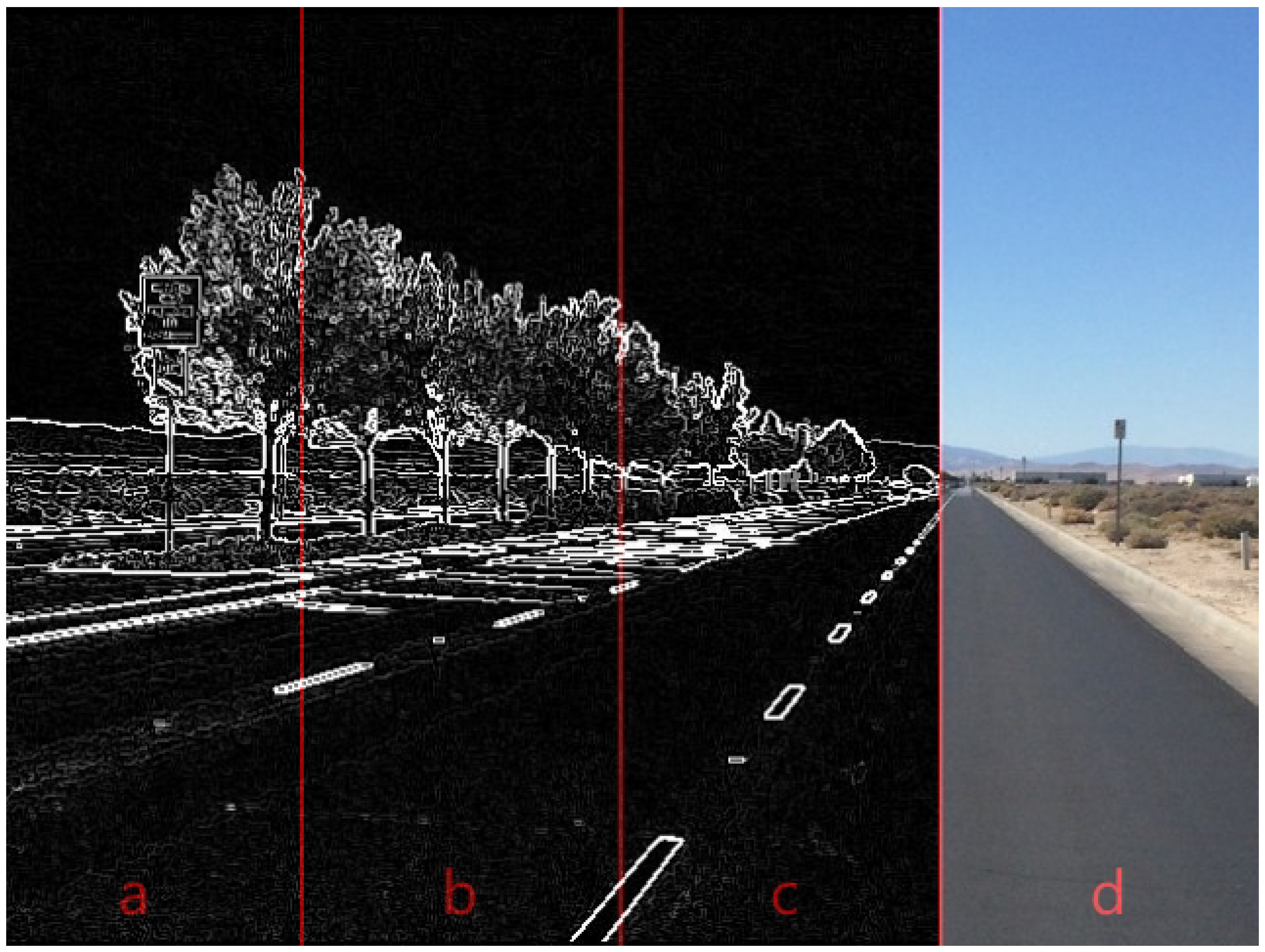
Figure 7 gives a typical processed image outcome partitioned in four subframes. The first subframe depicts the result of the Pynq-Z1 implementation and the second one the result of DE2-115 implementation. In the third subframe, we can see the outcome of the same algorithm running on a traditional CPU and in the fourth and final one, the original image. We need to address that our hardware designs provide accurate and convincing edge detection, identical to the output of the algorithm running on the CPU.
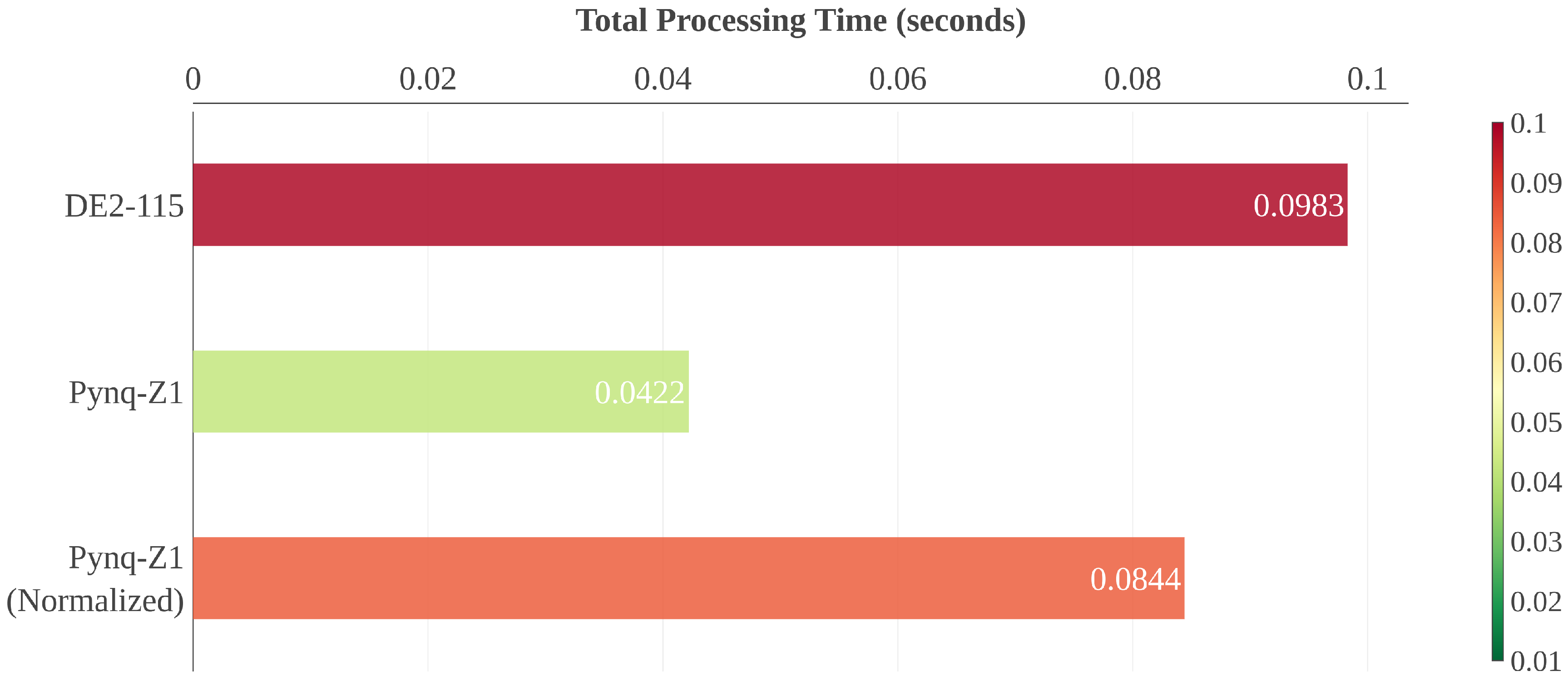
The processing time of the Pynq-Z1 implementation averaged around 0.0422 s per image and the DE2-115 implementation around 0.0983 s. However, the Pynq-Z1 board is running at 100 MHz instead of 50 MHz; thus, we provide a theoretical sample by degrading the Pynq-Z1 performance by half. The expected total processing time of the Pynq-Z1, running at a clock speed of 50 MHz, should be 0.0844 s (or 84 ms) approximately. The final result at the same clock speed is still better at the Pynq-Z1 board, resulting in a 14% faster computation time. There are several factors about this improvement, varying from the faster and more modern on-board components of the Pynq-Z1 to the HLS optimizations and better hardware utilization, which are discussed in the next section.
6. Discussion
Based upon our results, it seems that the HLS design performed slightly better in comparison with the bare VHDL implementation (
Figure 8). There are some minor hardware differences between the two platforms but we can safely assume that the HLS tools did an excellent job, producing a highly competitive design comparable and better than the manual counterpart. In addition, the HLS tool made a huge increase in productivity, since many of the supported hardware underlying functions (e.g., AXI4 protocol) are pre-implemented and ready to use.
With the correct configuration, the HLS tool produced highly optimized VHDL code for the specific design. The two combinational operators can be “chained” together in a single cycle by the designer, by performing operation scheduling within the target clock periods, so that false paths [
23] are avoided. It can reduce the number of bits required by datapath operators by making bitwidth optimization, reducing the area and power and increasing the performance of the design.
The HLS tool can also make use of the multiple BRAMs to store specific data structures to implement fast memory accesses at a low cost. These memory elements have a limited number of memory ports and the customization of memory accesses may require the creation of an efficient multi-bank architecture to avoid limiting the performance. In addition, there are numerous loop optimizations by pipelining, allowing a loop iteration to start before the completion of its predecessor, provided that data dependencies are satisfied. There are many more HLS optimizations besides the above, which do not affect our current design implementation, but in other cases may dramatically increase the performance [
24].
7. Conclusions
Unequivocally, the latest of the FPGA HLS tools have made significant progress in providing wide language coverage, robust compilation technology, platform-based modeling, and domain-specific system-level integration [
25]. As a result, they can quickly provide highly competitive Quality of Results (QoRs), in many cases comparable to or better than manual RTL designs. For the FPGA design community, it appears that HLS technology is transitioning from research and investigation to selected deployment [
26].
HLS tools feature several optimizations to improve the performance of the accelerators. Some of them are borrowed from the compiler community, while others are specific for hardware design. In this paper, we illustrate both the traditional and modern way of designing HDL blocks. Specifically, in the first part of the paper, we show a pure VHDL implementation and in the second one an HLS-based approach, and our results show that the HLS did a better optimization, in terms of performance and efficiency.


