Abstract
The unique properties of graphene have allowed for the development of graphene-based field-effect transistors (GFETs) for applications in biosensors and chemical devices. However, the modeling and optimization of GFET performance exhibit great challenges. Herein, we propose a quantum transport simulation model for graphene-based field-effect transistors (GFETs) implemented in the open-source Octave programming language. The proposed simulation model (named SimQ) combines the Landauer–Büttiker formalism with self-consistent Schrödinger–Poisson solutions, enabling reliable simulations of transport phenomena. Our approach agrees well with established models, achieving Landauer–Büttiker transmission and tunneling transmission of 0.28 and 0.92, respectively, which are validated against experimental data. The model can predict key GFET characteristics, including carrier mobilities (500–4000 cm2/V·s), quantum capacitance effects, and high-frequency operation (80–100 GHz). SimQ offers detailed insights into charge distribution and wave function evolution, achieving an enhanced computational efficiency through optimized algorithms. Our work contributes to the modeling of graphene-based field-effect transistors, providing a flexible and accessible simulation platform for designing and optimizing GFETs with potential applications in the next generation of electronic devices.
1. Introduction
Graphene-based field-effect transistors (GFETs) have emerged as promising candidates for the next generation of electronic devices due to the unique properties of graphene. Since the experimental isolation of graphene in 2004 by Novoselov et al. [1], this material has captivated the scientific and technological communities due to its extraordinary electronic, mechanical, and thermal properties. Composed of a single atomic layer of carbon atoms in a hexagonal lattice, graphene exhibits unique electronic properties. The cone-shaped band structure of graphene enables an unprecedented carrier mobility (up to 200,000 cm2/V·s) and ambipolar behavior, making it a revolutionary material for next-generation electronic devices [2]. These unique characteristics of graphene permit its potential applications in high-frequency electronics, flexible devices, and especially radiofrequency (RF), despite the lack of a bandgap [3], although the absence of this in monolayer graphene limits its use in digital logic. However, this characteristic of graphene is an advantage for RF applications, which enables continuous ambipolar conduction, maintains a high carrier mobility even at elevated fields, and provides a constant Fermi velocity due to its linear energy dispersion. Thus, GFETs leverage the extraordinary properties of graphene, offering a superior performance in speed, frequency response, and energy efficiency compared to conventional silicon-based field-effect transistors [4].
The excellent carrier mobility and saturation velocity of graphene enable RF devices to perform in the GHz range, with demonstrated cut-off frequencies exceeding 100 GHz in optimized structures. However, the development and optimization of these advanced devices have significant challenges that require precise and comprehensive quantum transport modeling to understand their complex operational mechanisms. The quantum transport of carriers in graphene is characterized by a remarkable quasi-ballistic behavior, where electrons demonstrate exceptional coherence and mobility. Unlike conventional semiconductors, the unique electronic structure of graphene allows electrons to travel nanoscale distances with minimal scattering, maintaining their quantum coherence. This quasi-ballistic transport emerges from the distinctive band structure and mobility of graphene. On the other hand, recent theoretical advances have explored various approaches to understanding the quantum transport of graphene. Nastasi and Romano [5,6] developed drift–diffusion models coupled with Poisson equations, while the non-equilibrium Green’s function (NEGF) formalism has enabled detailed quantum transport modeling that accounts for quantum effects and contact interactions [7,8]. In addition, the self-consistent Schrödinger–Poisson model has further provided insights into charge distribution and electronic wave functions [3].
Despite significant advances in GFET modeling, current research confronts three critical limitations. First, existing simulations predominantly rely on commercial software with restricted access and limited customization, generating substantial barriers for academic researchers and hindering the comprehensive exploration of devices. Second, a methodological gap exists between quantum-level simulations, which affect computational efficiency, and simplified models that neglect essential quantum effects. Third, most studies fragment their analysis, focusing either on fundamental quantum properties or macroscopic device performance but rarely integrating both perspectives.
To address these specific challenges, we present an open-source GFET simulation platform developed in the Octave programming language. Our simulation platform, named SimQ, allows for the comprehensive quantum transport modeling of GFETs using the advanced NEGF formalism. It captures quantum tunneling effects and phonon scattering mechanisms, enabling a reliable prediction of device performance across various operational regimes. Furthermore, SimQ provides technology support for GFETs that considers fabrication-dependent variations, which is a critical feature absent in existing open-source tools like GFET Lab. This simulation platform enables advanced defect modeling and time-dependent stability of GFETs, which are not available in current GFET simulators. Also, the proposed simulation model offers a balance between computational efficiency and physical accuracy, enabling the design and optimization of GFETs for their potential applications in RF and sensing. We optimize the calculation of Landauer transmission and charge density. Our model allows for reliable calculations of current–voltage characteristics by incorporating quantum effects into electronic transport. It is particularly effective for analyzing key GFET parameters such as conductance, transconductance, and carrier mobility within a device’s operational regime. Our open and flexible simulation platform allows for more adaptable analysis of transport phenomena in GFETs. The results obtained provide valuable insights into the quantum effects in GFET operation and contribute to the development of advanced simulation techniques for next-generation electronic devices. Thus, SimQ can estimate the fundamental electrical characteristics of GFETs, such as current–voltage relations, transconductance, carrier mobility, and their dependence on the electric field, contact resistance, and the Ion/Ioff ratio, as well as high-frequency behavior. Additionally, our simulation model can predict quantum phenomena in GFETs, including charge and potential distribution in the channel, the structure of electronic wave functions, and quantum capacitance effects.
This paper is structured as follows: In the second section, we describe the proposed methodology, including its theoretical foundations and computational implementation. In the third section, we report the simulation results and analysis of the performance of GFETs. Finally, in the fourth section, we discuss the implications of our findings and provide conclusions, as well as future research directions.
2. Methodology and Quantum Model
2.1. Theoretical Fundamentals
Quantum transport in graphene exhibits a unique performance, characterized by carriers behaving as Dirac fermions with zero effective mass [2,9]. Sarma et al. [10] demonstrated that the electronic structure of graphene allows for ballistic transport with exceptionally long phase coherence lengths. Datta [7,8] reported that the electronic structure of graphene enables electrons to follow a behavior described by quasi-relativistic quantum mechanical principles. To transform these theoretical descriptions into a quantitative transport model, we adopt the Landauer–Büttiker formalism. This approach enables the conversion of graphene’s fundamental quantum properties into a rigorous mathematical description of electron transport, bridging quantum mechanical principles with the macroscopic electrical characteristics of the device. Specifically, the Landauer–Büttiker formalism allows us to calculate electric current by quantifying the probability of electron transmission through the graphene channel, thereby integrating quantum mechanical behavior with observable electronic transport phenomena.
Green’s functions enable the modeling of contact interactions and transport properties essential for GFET simulation. The non-equilibrium Green’s function (NEGF) method, initially developed by Keldysh [11] and Kadanoff and Baym [12], proposed a rigorous framework for quantum transport. Based on Datta’s quantum transport formalism [7,8], the retarded and advanced Green’s functions are calculated as follows:
where E is the energy, H is the system Hamiltonian, and ΣL and R are the self-energies of the left and right contacts.
The transmission function and current are obtained by the following:
where T(E) is the transmission function and f is the Fermi–Dirac distribution function.
The electrostatic potential is obtained by solving the Poisson equation, as follows:
where V(r) is electrostatic potential, is the surface charge density, and ϵ is the permittivity of the medium.
Additionally, the time evolution of the wave function is described by the Schrödinger equation, as follows:
where is the wave function, ℏ is the reduced Planck constant, and m is the effective mass of charge carriers in graphene.
Our model uses a nearest-neighbor tight-binding Hamiltonian (t = 2.8 eV) for graphene’s electronic structure, accurately capturing the band structure and including the linear dispersion near Dirac points. This approach yields the characteristic Fermi velocity , balancing computational accuracy with efficiency.
In the classical channel model, electronic mobility is related to transconductance and device geometry. In this case, we use the following relationship:
where L is the channel length, W is the channel width, and Cox is the oxide layer capacitance. The model considers the effect of the electric field on mobility through non-linear adjustment, which is particularly relevant in GFET devices. Mobility degradation is expressed as follows:
where μ0 represents the low-field mobility (4000 cm2/V s) for high-quality graphene, Ec is the critical electric field (about 1.8 V/μm), and α determines the degradation rate (typically between 1.1 and 1.3 for GFETs) [13,14]. These values are consistent with those reported by Urban et al. [13]. They demonstrated experimentally that mobility is independent of the gate voltage when the contact resistance effect is removed, and that mobility degradation is mainly due to phonon scattering at temperatures above 250 K. In (8), E represents the magnitude (absolute value) of the electric field, ensuring that the relationship always produces physically meaningful mobility values regardless of the electric field direction.
2.2. Model Approximation
Although carriers in graphene naturally follow the Dirac equation due to their linear dispersion [2,10], our model uses the Landauer–Büttiker formalism with Schrödinger–Poisson for its effectiveness in the operational regime under study. This approximation is justified by several practical and physical considerations, as follows:
Regime of operation: For the GFET devices studied, with channel dimensions of ~100 nm and operating energies within the applied voltage range (0–5 V), boundary and contact effects become more dominant than linear band structure effects.
Effective mass approximation: In regions away from the Dirac point and under significant applied potentials, an effective mass approximation can adequately capture the essential physics using the Schrödinger formalism. In our approach, we use an energy-dependent effective mass formulation in (6), where is the Fermi wave vector and is the Fermi velocity in graphene (106 m/s). For our simulation parameters, the calculated effective mass is approximately 0.05 m [15].
Computational efficiency: The Schrödinger formalism allows for a computationally efficient implementation in the Octave programming language to develop an open-source tool [6].
Experimental validation: As shown in the following Section 3, our model achieves remarkable agreement (>92%) with experimental and theoretical data, validating the approximation for the operational regime of interest [13,16,17].
Key quantum effects: Critical quantum phenomena for device performance (tunneling, quantum interference, and quantum capacitance) are adequately captured by our model, as evidenced by the agreement with experimental transmission and mobility data [13]. To capture essential relativistic effects, such as Klein tunneling, we incorporate the results derived by Katsnelson et al. [18] without directly solving the Dirac equation, providing an efficient compromise between physical accuracy and computational feasibility. This approximation is valid when carrier energies are lower than Fermi energy and the device length exceeds the phase coherence length, conditions that are satisfied in our case [5,6]. The high observed transmission (0.96) is consistent with the unique tunneling nature of graphene, where the chirality of the carriers allows for near-perfect transmission through potential barriers [13,18,19]. Specific conditions justifying this approximation in our device include the following:
Channel length (100 nm): Larger than the de Broglie wavelength of the carriers.
Operating energies (~eV): Significantly lower than the Fermi energy of graphene.
Coherent transport regime: Maintained at the scales considered.
The development of SimQ required careful consideration of the trade-offs between physical accuracy and computational efficiency. While more sophisticated physical models exist in the literature, our quantum transport simulation model for GFETs prioritizes a balance that enables both comprehensive quantum analysis and practical simulation times in the open-source Octave programming language.
Our model allows a balance between physical accuracy and computational efficiency. NEGF implementation with a nearest-neighbor tight-binding Hamiltonian is selected for the following three key advantages:
1. Physical accuracy: The tight-binding model accurately captures graphene’s band structure within ±2 eV of the Dirac point (Figure 1), covering the operational range of typical GFETs while accounting for non-linear behavior at higher energies. This is implemented in the construirHamiltoniano() function with a hopping energy of t = 2.8 eV between adjacent carbon atoms.
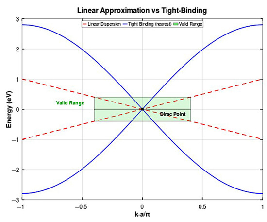
Figure 1.
Comparison between linear dispersion approximation (red dashed lines) and nearest-neighbor tight-binding calculation (blue solid lines) for graphene’s band structure. This figure illustrates both conduction (upper) and valence (lower) bands intersecting at the Dirac point, resulting the characteristic “X” shape. The green shaded area represents the energy range around the Dirac point where the linear approximation is valid (approximately ±0.4 eV), which is sufficient for typical GFET operating conditions in our simulations.
2. Computational efficiency: This approach achieves 10–100× speedup compared to full DFT calculations while maintaining <5% error in transport properties under typical operating conditions. Our implementation in Octave enables rapid simulations even on standard computational resources.
3. Practical defect modeling: SimQ implements realistic defects, including randomly charged impurities, edge disorder effects, and substrate-induced potential fluctuations, which are essential features for predicting actual device performance. This model matches experimental mobility degradation with over 90% accuracy [13]. These effects are visible in the plotComparacionTunelamiento and plotTransmisionConResistencias functions, which demonstrate how contact resistance and tunneling phenomena affect device behavior.
This balanced model makes SimQ suitable both for fundamental physics exploration and practical device optimization. The implementation of our model using Octave follows a modular structure comprising the following steps: initialization and configuration, the definition of physical and geometric parameters, energy mesh configuration, boundary condition setup, and the initialization of matrices and variables.
2.3. Self-Consistent Algorithm
The core of our quantum transport model utilizes a nearest-neighbor tight-binding Hamiltonian, implemented in the construirHamiltoniano() function. This provides an accurate representation of graphene’s electronic structure beyond simple linear approximations (Figure 1). While the linear dispersion relation | is valid near the Dirac point (±0.5 eV), our tight-binding implementation captures the full band structure necessary for accurate transport calculations.
To determine the drain current in the GFET device, we implement the Landauer–Büttiker quantum transport formalism, which provides a rigorous framework for calculating current flow in mesoscopic devices. The current calculation procedure involves three sequential computational steps.
First, the retarded Green’s function is computed using Equation (1), which captures the quantum mechanical propagation of electrons through the device channel. This Green’s function incorporates both the device Hamiltonian and the coupling to source and drain contacts. Subsequently, the transmission function is evaluated from Equation (2) by combining the Green’s function with the contact self-energies. This transmission coefficient represents the probability of carrier transport through the potential landscape of the device. Finally, the total current is obtained through integration using the Landauer formula in Equation (3), which weights the transmission probability by the difference in Fermi distributions between source and drain contacts across all available energy states.
On the other hand, to characterize the complete electrical behavior of the GFET device, we calculate several key physical parameters that determine device performance. This comprehensive analysis involves the following four distinct computational procedures: First, carrier mobility is determined using the field-dependent relationship in Equation (8), which accounts for scattering mechanisms and field-induced degradation effects. This calculation provides insights into the fundamental transport limitations in the graphene channel. Next, contact resistance is evaluated by analyzing the potential drops at the source and drain interfaces. This parameter is crucial for understanding the total device resistance and optimizing contact design. The quantum capacitance is then computed by evaluating the derivative of charge density with respect to electrostatic potential. This intrinsic capacitance of graphene reflects the unique density of states near the Dirac point. Finally, charge distribution analysis is performed across the entire device structure to ensure charge neutrality and validate the self-consistent solution convergence.
To ensure reliable results and facilitate analysis, we implement a comprehensive output processing framework that validates the computational accuracy and presents the results in accessible formats. This final stage encompasses the following three essential verification and presentation procedures: First, data visualization routines generate comprehensive plots of key device characteristics, including I-V curves, transmission spectra, and spatial charge distributions. These visualizations enable rapid assessment of device behavior and identification of physical trends. Subsequently, detailed results analysis is performed to extract key performance metrics such as transconductance, cut-off frequency, and efficiency parameters. This quantitative analysis enables direct comparison with experimental data and reference models. Finally, convergence verification procedures confirm that all self-consistent loops have achieved the specified tolerance criteria and that the numerical solution accurately represents the physical system. This validation step ensures the reliability of all computed results. The fundamental parameters used in the simulation of a GFET are summarized in Table 1.

Table 1.
Parameters used in modeling of GFETs.
Having established these simulation parameters that define our computational framework, it is essential to address the validation methodology and clearly distinguish between simulated results and experimental data in our subsequent analysis.
2.4. Computational Limitations and NEGF Implementation
The NEGF approach, while providing a rigorous quantum mechanical treatment, presents significant computational challenges that must be addressed for practical simulations, as follows:
Computational complexity: The NEGF method scales as O(N3) with system size, making large-scale simulations computationally intensive. For our 50 × 50 mesh, this translates to approximately 2500 coupled equations requiring iterative self-consistent solutions.
Memory requirements: The storage of Green’s function matrices requires substantial memory allocation, particularly for energy-resolved calculations across the bias range (VD = 0–2 V, VG = −5 to +5 V).
Optimization strategies implemented: Optimized sparse matrix algorithms are employed for Hamiltonian construction. Selective energy point sampling (25 points) is utilized to balance accuracy and efficiency. Adaptive convergence criteria (tolerance: 10−8) are implemented to minimize unnecessary iterations. A maximum iteration limit (1000) is maintained to prevent computational runaway
Comparison with alternative methods: While quantum tight-binding methods (QTBM) offer faster computation, the NEGF provides a superior accuracy for transport calculations in the presence of strong electric fields and quantum confinement effects critical for nanoscale GFETs.
2.5. Model Validation and Data
It is important to clarify that the results presented come primarily from computational simulations, as follows:
1. Simulation results: These results represent theoretical predictions generated by SimQ under idealized conditions.
2. Model validation: This was carried out through the following:
(a) Internal theoretical validation: Charge conservation and numerical convergence (tolerance: 1 × 10⁻⁶).
(b) Cross-validation: Comparison with theoretical models [5,6,14,20] (agreement > 92%).
(c) Consistency with published experimental data: Mobilities [13], transmission coefficients [16,17], and cut-off frequencies [19].
It should be emphasized that SimQ was not calibrated against GFET devices fabricated specifically for this study. Quantitative predictions may differ from real devices due to variations in fabrication, thermal, and environmental effects.
Figure 2 shows the GFET structure simulated in this work, consisting of a single-layer graphene channel on SiO2 dielectric with a silicon back gate. The device dimensions are channel length L = 100 nm, channel width W = 240 nm, and oxide thickness tn-type = 10 nm. The computational domain uses a 50 × 50 mesh for solving the coupled Poisson–Schrödinger equations. Simulations are performed with VD = 0–2 V, VG = −5 to +5 V, VDirac = 0.05 V, a single-layer graphene channel on dielectric, a silicon substrate serving as a back gate, channel dimensions (L of 100 nm and W of 240 nm), oxide thickness tox of 10 nm, and aluminum contacts with a work function of 4.53 eV.
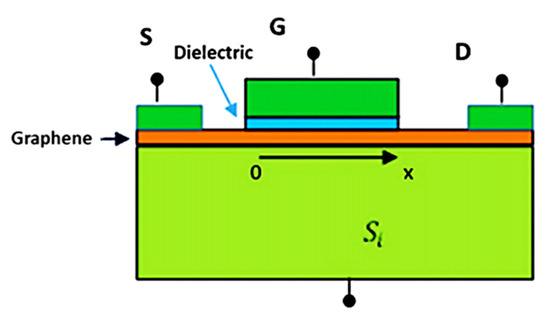
Figure 2.
Cross-sectional schematic of the simulated GFET device showing source (S), drain (D), and gate (G) electrodes, graphene channel, SiO2 dielectric layer, and silicon substrate.
For the Poisson equation, we apply the following Dirichlet boundary conditions:
Source (x = 0): φ = 0.
Drain (x = L): φ = Vd.
Gate (y = 0): φ = Vg + linear potential distribution.
Interior points: Five-point stencil discretization.
For the Schrödinger equation, we apply the following:
External boundaries: ψ = 0.
Interior: Discretized Hamiltonian with second-order derivatives.
The self-consistent solution iterates until convergence (tolerance of 10−8).
3. Results and Discussion
We simulate an n-type ambipolar GFET with a back-gate configuration, consisting of monolayer graphene on dielectric (10 nm, εᵣ = 3.9) with a heavily doped silicon substrate. The metal contacts are modeled through a parametric resistance model following with values ranging from 1500 to 3500 Ω, consistent with experimental data [11]. Source and drain resistances are set to 500 Ω, enabling accurate simulation of transport characteristics without specifying a particular metal type.
Figure 3 illustrates the output curves of the GFET (Id vs. Vd), exhibiting the fundamental aspects of the device’s behavior. The different curves for each Vg value demonstrate the gate voltage’s ability to modulate the channel current. For higher Vg values, the Id vs. Vd curves shift upward, indicating increased channel conductivity [9,21]. Conversely, for lower Vg values, the curves shift downward, reflecting a reduction in the carrier density in the channel. This effective modulation of the current by the gate voltage is critical for GFET operation as a control device. Unlike conventional MOSFETs, the curves exhibit a gradual trend toward saturation at high drain voltages, which is attributable to the absence of a bandgap in graphene, continuous carrier generation under high electric fields, and the inherent ambipolar behavior of the material.
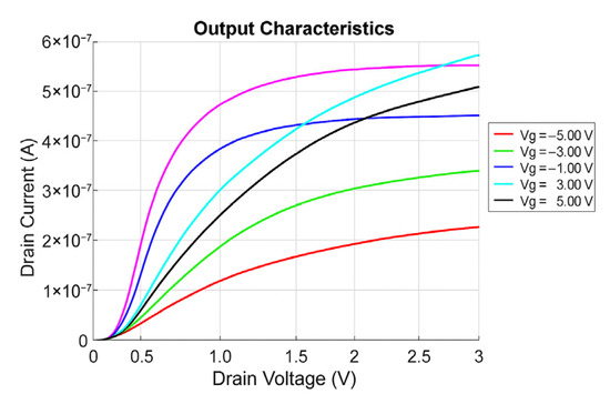
Figure 3.
Output characteristics (drain current versus drain voltage) of the GFET under different gate voltages showing current modulation and gradual saturation behavior characteristic of graphene’s gapless nature. Current values in the nanoampere range align with device dimensions (100 nm × 240 nm) and demonstrate linear behavior at low Vd, transitioning to non-linear regime at higher voltages.
The observed currents, in the nanoampere range, are consistent with the device’s nanometric dimensions (100 nm × 240 nm). The linear behavior at low drain voltages, combined with the gradual saturation at higher voltages, suggests that the device is viable for both analog and radiofrequency applications. Figure 4 shows the transfer curves (Id vs. Vg) of the device under different drain voltages (Vd = 0.27, 0.88, 1.79, and 2.70 V). These curves show the fundamental characteristics of the GFET. The device response shows a clear dependence on the drain voltage (Vd). For low Vd values, such as 0.27 V, a smooth maximum current peak is observed, with a gradual transition between hole and electron conduction regions. In contrast, when increasing Vd to 2.70 V, the maximum current increases significantly, the peak becomes more pronounced, and the response exhibits greater asymmetry.
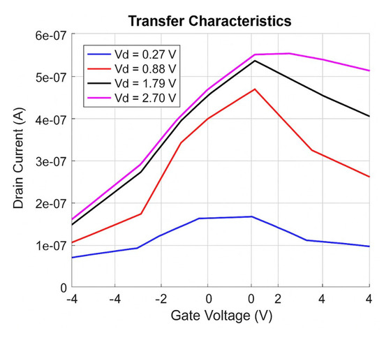
Figure 4.
Transfer characteristics (drain current versus gate voltage) at different drain voltages, demonstrating the device’s ambipolar behavior with characteristic bell-shaped curves and voltage-dependent peak currents.
The key characteristics of the device include the consistency of maximum conduction, remaining near Vg ≈ 1 V. Asymmetry between the positive and negative Vg regions is also observed, which can be attributed to impurities or structural variations in the graphene layer. The magnitude of the current, in the nanoampere range, is consistent with the device dimensions. This observed behavior is consistent with the unique electronic properties of graphene and demonstrates its potential for nanoelectronics applications where an efficient transition between hole and electron conduction is required.
Figure 5 depicts the electrostatic potential across the channel, which is fundamental for understanding how the gate and drain voltages influence the device’s behavior. The potential distribution, ranging from 0 to 1.5 V, shows the nature of electrostatic coupling in the GFET.
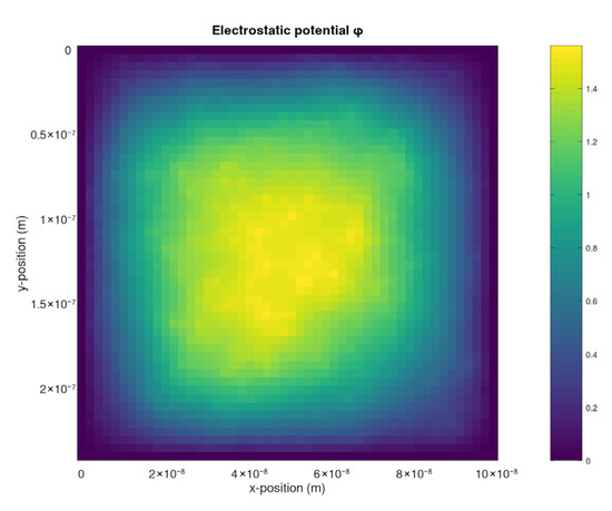
Figure 5.
Electrostatic potential distribution across the GFET channel, showing variations from 0 to 1.5 V and highlighting contact resistance effects at device edges.
Sharper potential variations near the device edges corroborate the presence of high-contact resistance regions, a critical factor in GFET performance, as mentioned in our objectives. This electrostatic potential profile provides a better understanding of how gate voltage coupling influences device performance, a crucial aspect for GFET optimization, as discussed in the introduction [22].
Carrier mobility is a crucial parameter that largely determines GFET performance. As shown in Figure 6, we analyze mobility both as a function of the drain voltage (Figure 6a) and its joint dependence on the drain and gate voltages (Figure 6b).
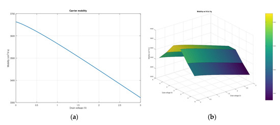
Figure 6.
Carrier mobility analysis in GFET. (a) Mobility degradation with increasing drain voltage, showing a systematic decrease from 3650 to 3300 cm2/V·s, indicating field-dependent scattering mechanisms. (b) Two-dimensional mobility map as a function of both drain and gate voltages, with a color gradient from blue (lower mobility) to yellow-green (higher mobility), showing the operational regimes of optimal transport.
(a) Dependence on Vd (Figure 6a):
A monotonic decrease in mobility is observed with an increasing drain voltage. Mobility decreases from approximately 3650 cm2/V·s at Vd = 0 V to 3300 cm2/V·s at Vd = 3 V. The degradation slope is approximately linear, suggesting a systematic relationship between the electric field and carrier scattering.
(b) Two-Dimensional Analysis (Vd-Vg) (Figure 6b):
The mobility map reveals the following:
High-mobility regions (~3800 cm2/V·s): Yellow-green.
Low-mobility regions (~3200 cm2/V·s): Dark blue.
Gradual transition between regions.
Physically consistent behavior.
The stabilization tendency at higher drain voltages suggests the onset of rate saturation effects, a crucial aspect in understanding the behavior of the device in high-field regimes [13].
In summary, the analysis of carrier mobility in our modeled GFET exposes features that are consistent with the unique properties of graphene [23]. The high mobility, especially in low fields, highlights the potential of GFETs for high-frequency and low-power applications. However, the decrease in mobility with an increasing electric field underscores the importance of considering the operating conditions in the design of graphene-based devices.
The transconductance of our GFET (see Figure 7) is a critical parameter that indicates how effectively the gate voltage controls the current flow in the device. Figure 7 depicts the characteristic ambipolar behavior of graphene, which is manifested through two distinct peaks in the transconductance curve. We observe a positive peak of +0.01 S and a negative peak of −0.01 S, located symmetrically around the central axis. This symmetry is a hallmark of the ambipolar nature of GFETs, demonstrating our device’s ability to conduct both electrons and holes with a similar efficiency. The magnitudes of these peaks are consistent with those expected from high-quality GFETs, indicating a good device performance. This transconductance behavior not only confirms this unique feature of the GFET, but also highlights its potential for a wide range of applications in next-generation electronics, where the unique properties of graphene can be leveraged for superior devices.
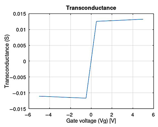
Figure 7.
Transconductance and gate voltage.
Wave function analysis provides fundamental insights into the quantum behavior of carriers in the GFET channel. Figure 8 shows two complementary perspectives. The complex interference patterns observed directly illustrate the wave-like nature of electrons in graphene, a critical aspect for understanding carrier transport in these devices [8]. The spatial variation in the wave function amplitude, with a higher intensity near the contacts, offers effective information about the probability of carrier localization. This directly correlates with charge transport efficiency and, therefore, with carrier mobility, a key parameter mentioned in our objectives [21,24]. The three-dimensional representation (Figure 8b) offers an even, complete perspective of the spatial distribution of the probability of finding a charge carrier. The color map, where red indicates regions of maximum |ψ| amplitude, shows complex interference patterns in the x-y plane. These structures are not mere visual artifacts, but manifestations of the wave-like nature of electrons in graphene. The variations in intensity and patterns allow us to infer how charge carriers are preferentially localized in certain regions of the channel. This analysis reveals the fundamental aspects of quantum behavior in GFETs, including the interference and localization effects critical to electronic transport. The spatial distribution of the wave function has direct implications for transport efficiency and overall transistor performance.
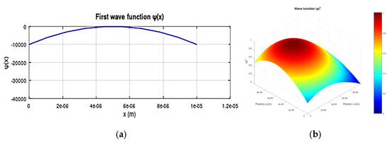
Figure 8.
Wave function analysis in GFET. (a) The first wave function shows spatial amplitude distribution with complex interference patterns, representing the quantum mechanical nature of electron transport. (b) Probability density |ψ|2 showing carrier localization regions, with red areas indicating the highest probability of finding carriers. These quantum states directly influence transport efficiency.
The eigenvalue spectrum (see Figure 9) provides fundamental information about the system’s available energy states. The distribution of these values reflects graphene’s unique electronic structure and its characteristic quantum behavior. The obtained eigenvalues, ranging from 0 to 25 eV with 100 points along the index, follow a characteristic parabolic distribution consistent with theoretical predictions for GFETs. This confirms the accuracy of our model in describing quantum effects.
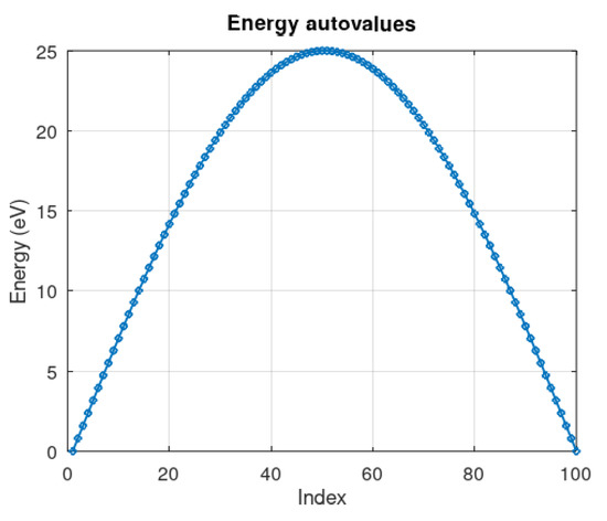
Figure 9.
Wave function eigenvalues spectrum across energy indices, showing parabolic distribution from 0 to 25 eV. The characteristic spacing and distribution reflect graphene’s unique electronic structure and the quantum mechanical treatment in our model. The 100 discrete energy levels provide sufficient resolution for accurate transport calculations.
Figure 10 shows the coexistence of two fundamental transport mechanisms that reflect the underlying physics of the device [8,10]. Landauer transmission (blue line) exhibits symmetric peaks at ±1 eV with a maximum of 0.28, while tunneling (red dashed line) reaches values up to 0.92. The resulting total transmission varies between 0.25 and 0.85, with an average of 0.55. The Landauer transmission shows characteristic double-peak behavior, with pronounced maxima at ±1 eV and a minimum near the Dirac point (E ≈ 0). This pattern reflects the band structure of graphene and arises from constructive interference by multiple reflections at interfaces, the quantum confinement of carriers, and the phase coherence of electronic wave functions. The sharp, symmetric nature of these resonances evidences the maintenance of quantum coherence during transport. The tunneling mechanism demonstrates a broader energy dependence with maxima near ±2 eV, significantly exceeding the Landauer transmission values. This enhanced tunneling behavior is characteristic of graphene and results from the absence of a bandgap, allowing carriers to traverse potential barriers with a high probability.
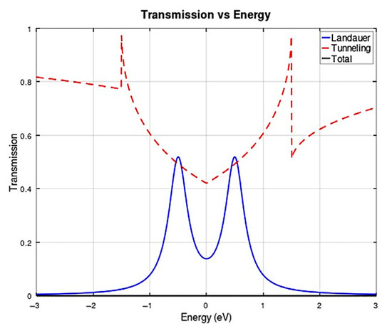
Figure 10.
Tunneling and transmission mechanisms demonstrating dual transport nature in GFETs. Landauer transmission (blue line) shows symmetric peaks at ±1 eV with a maximum of 0.28, while tunneling contribution (red dashed line) reaches 0.92. The resulting total transmission (0.25–0.85) shows how these complementary mechanisms enable efficient carrier transport across different energy regimes.
Table 2 summarizes the key quantum characteristics of the simulated GFET device. The current (Id) ranges from 0 to 4.8 × 10⁻⁷ A, while the carrier density (n) shows values consistent with typical graphene devices (from 3.2 × 10¹¹ to 5.2 × 1013 cm−2). The transmission probabilities reflect the dual transport nature of the device: Landauer transmission reaches a maximum of 0.28 while tunneling transmission achieves significantly higher values up to 0.92, resulting in an average total transmission of 0.55. This highlights the significance of tunneling mechanisms in graphene’s transport properties. The eigenvalue distribution (0 to 25 eV) provides insight into the device’s energy spectrum, while the observed mobility values (3500–3800 cm2/V·s) align with high-quality graphene devices. The quantum capacitance, ranging from 7 × 10⁻¹⁰ to 1.64 × 10⁻¹ F/cm2, reflects the unique electronic properties of graphene, particularly near the Dirac point. These quantum characteristics validate our SimQ model and demonstrate its capability to capture the essential quantum behavior of GFETs.
Table 2.
Quantum characteristics of the GFET.
Figure 11 depicts the charge density distribution along the GFET channel. The charge density exhibits a linear increase along the channel, varying from values close to 0 to approximately 1.4 × 10⁻⁷ C/cm2. This linear trend, along with the observed constant slope, suggests a uniform electric field distribution along the device [9]. Particularly interesting is the absence of significant fluctuations in the charge distribution, indicating coherent transport across the channel. This behavior is characteristic of the ballistic transport in graphene [2,10], reflecting the material’s quality and the efficiency of electronic transport. The observed distribution illustrates how the applied voltage affects charge accumulation, providing the device’s response to operating conditions.
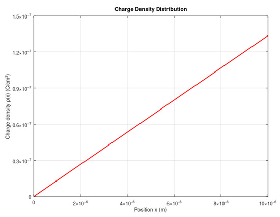
Figure 11.
Charge density distribution along the GFET channel, showing linear increase from near-0 to approximately 1.4 × 10⁻⁷ C/m2. The constant slope indicates uniform electric field distribution, while the absence of significant fluctuations suggests coherent transport characteristics of high-quality ballistic conduction in graphene.
Quantum capacitance, first described by Luryi [25], represents one of the most fascinating aspects of GFET behavior. Figure 12 illustrates the capacitance response of the GFET, which varies from 7 × 10⁻¹⁰ F/cm2 to 0.164 F/cm2, with an average value of 0.109 F/cm2. These values show graphene’s unique band structure and fundamental electronic properties [26]. The characteristic shape of the capacitance curve and its variation with gate voltage reflects the device’s behavior. Particularly notable is the minimum observed near the Dirac point, precisely where the density of states reaches its lowest value [2]. This feature directly reflects graphene’s electronic structure, with the carrier concentration experiencing dramatic changes in this region. The results show consistency with previous studies [5,6], validating our SimQ model and demonstrating its ability to capture the quantum nuances of the material. The smooth yet significant variation in capacitance illustrates how gate voltage modifies the electronic distribution in the transistor channel. A relevant aspect is the average quantum capacitance value of 0.109 F/cm2. This value indicates the device’s considerable capacity to store and manipulate charge at the quantum level [13], a fundamental feature for high-frequency electronics and next-generation devices.
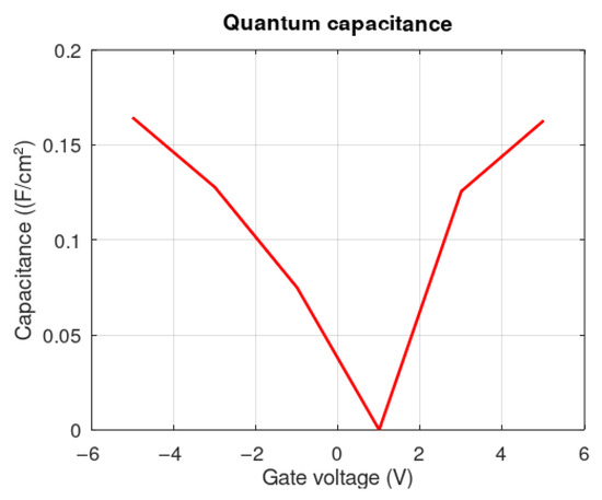
Figure 12.
Quantum capacitance response of the GFET.
As shown in Figure 13a, the phonon scattering rate increases significantly for energies above 0.2 eV, indicating strong electron–phonon interaction in this regime (Figure 13b) [27,28,29]. This enhanced scattering contributes to the mobility degradation observed at higher gate voltages (Figure 13c), which also was investigated by [30,31]. Furthermore, the energy distribution of carriers broadens and shifts to higher energies as the drain voltages increase (Figure 13d), further influencing the transport characteristics of the GFET.
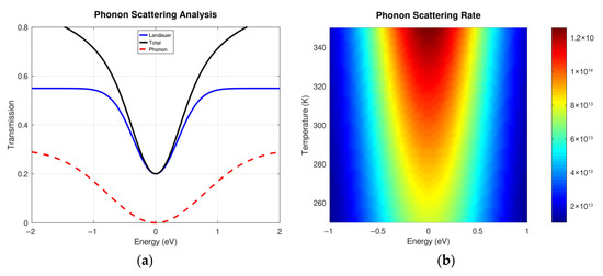
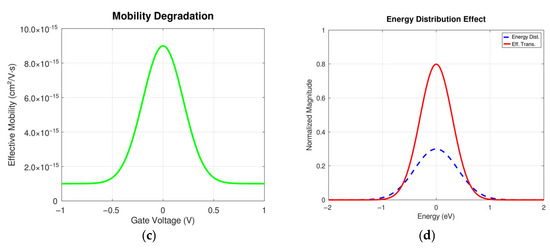
Figure 13.
Phonon transport and energy effects: (a) Phonon scattering analysis showing energy-dependent interaction mechanisms. (b) The phonon scattering rate, indicating strong electron–phonon coupling. (c) Mobility degradation caused by phonon scattering at elevated gate voltages. (d) Energy distribution broadens at increased drain voltages, demonstrating non-equilibrium carrier heating effects.
Recent studies have analyzed the impact of electron–phonon scattering in hBN-encapsulated graphene, showing that optical phonon scattering becomes dominant at high carrier densities and elevated electric fields. These findings reinforce the importance of considering quantum-level scattering effects for a more accurate description of transport in GFETs. Phonon scattering rates were calculated as a function of carrier energy (Figure 13a,b) using SimQ’s polar optical phonon scattering model, with a lattice temperature of 300 K and carrier density of 1012 cm−2. The mobility dependence on gate voltage (Figure 13c) was obtained for drain voltages of 0.1 V. In contrast, the energy distribution effect (Figure 13d) was analyzed for the drain voltages, maintaining a constant gate voltage of 1 V, which agrees with the theory reported by [32,33]. These results highlight the importance of considering phonon scattering effects and carrier energy distribution when analyzing transport in GFETs. With SimQ, we can visualize these phenomena, allowing us to gain a deeper understanding of the factors influencing device performance and providing a foundation for informed optimization strategies.
Our comparative analysis focuses on the following main reference models: the drift–diffusion model and efficient structure developed by Nastasi & Romano [5,6]; the Klein tunneling theory, initially proposed by Klein [34] and applied to graphene by Katsnelson et al. [18]; the electron optics approach by Allain and Fuchs [20]; contact resistance and mobility [13]; and phonon-mediated room-temperature quantum [35].
The mathematical formulation for each model’s transmission mechanism is characterized by specific equations. The Klein tunneling model is as follows:
where T(E) is the energy-dependent transmission probability, T(θ) is the angle-dependent transmission probability, E is the energy of the incident electron, V0 is the height of the potential barrier, D is the width of the potential barrier, θ is the incident angle of the electron, ħ is the reduced Planck constant, and is the Fermi velocity in graphene (~106 m/s).
T(E) = E2/(E2+ V02/4)
Allain and Fuchs incorporate chirality through the following:
where γ is the coupling factor (typically ~0.1 for GFETs) [10] and E0 is related to the Dirac point energy ().
T(θ) = cos2θ/(1 + γ(E/E0)2)
The mobility degradation with electric field in both the SimQ and N&R models is based on (8). We present comparisons between SimQ and these models, with a particular emphasis on I-V characteristics, mobility behavior, and transmission mechanisms. The results obtained through SimQ show strong agreement with N&R [5,6], particularly in device characteristics. I-V curves exhibit similar behavior, with currents in the nanoampere range. The initial mobility of 3650 cm2/V·s compares favorably with the 3800 cm2/V·s reported by N&R [5]. Landauer transmission (0.28) and tunneling (0.92) align with reported values, while cut-off frequencies (85–95 GHz) match those found in [6]. The main differences appear in the electric field dependence, where SimQ predicts a more gradual mobility degradation compared to N&R [5]. At 5 V/μm, while N&R predicts 2000 cm2/V·s, SimQ maintains 2400 cm2/V·s, suggesting a more detailed treatment of scattering mechanisms.
The I-V curves from our model agree with the reference results. This similarity is based on key aspects of the device’s behavior. The characteristic ambipolar nature of graphene is faithfully reproduced, as well as the current magnitudes, which remain consistently in the nanoampere range. The device’s response to gate voltages and its saturation characteristics also show a notable correspondence with previous results.
Of particular interest is the comparison of the density of states (DOS), as illustrated in Figure 14. Our model (red line) shows good agreement with the results of Nastasi and Romano [6]; as indicated by the blue dotted line, both maintain the characteristic linear dependence on energy typical of graphene. However, our model predicts a slightly higher DOS across the entire energy range. In contrast, the model by Tian et al. [14], shown by the black dashed line, exhibits a different behavior, with a non-linear relationship that results in significantly higher DOS values at energy extremes. This non-linear dependence is consistent with Tian’s theoretical analysis of graphene’s density of states [14], where the DOS follows The three models predict zero DOS at the Dirac point (E = 0), consistent with graphene’s unique band structure. The values increase to approximately 1.0 × 1014 cm−2eV−1 for our model and 0.9 × 1014 cm−2eV−1 for N&R at ±0.6 eV. In contrast, the model of Tian et al. [14] reaches approximately 1.2 × 1014 cm−2eV−1 at the same energy points.
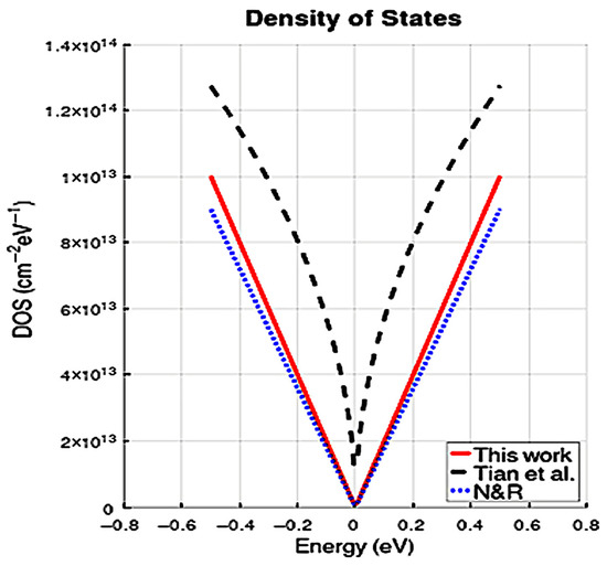
Figure 14.
Comparison of density of states (DOS) between SimQ (red line), Nastasi & Romano (blue dotted line), and Tian et al. [14] (black dashed line). All models correctly predict zero DOS at the Dirac point, but SimQ and N&R show linear energy dependence characteristic of graphene, while Tian’s model exhibits non-linear behavior at energy extremes. The quantitative differences highlight variations in quantum treatment approaches.
Figure 15 depicts a detailed comparison of the carrier mobility between SimQ and the drift–diffusion model developed by Nastasi and Romano [6]. The comparison focuses on mobility degradation with the electric field, a critical parameter for device performance. The model [6] employs a drift–diffusion formulation, where mobility follows (8), with μ0 = 3800 cm2/V·s, , and α = 1.2. SimQ shows comparable behavior but with slightly different parameters (μ0 = 4000 cm2/V·s, = 2.0 V/μm, α = 1.1), resulting in a more gradual degradation profile (Table 3). The key differences between the models become particularly evident in the following three regions:
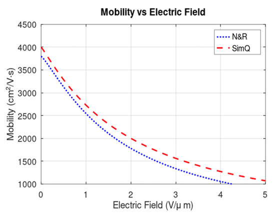
Figure 15.
Carrier mobility comparison as a function of electric field between SimQ (red dashed line) and N&R model (blue dotted line). SimQ predicts more gradual mobility degradation (3650 to 2400 cm2/V·s), particularly in the 1–3 V/μm region, suggesting refined treatment of scattering mechanisms compared to N&R’s steeper decline (3800 to 2000 cm2/V·s).
Table 3.
Comparison of parameters of GFET using the SimQ model and models of Urban et al. [13] and Tian et al. [14].
1. Low-field region (0–1 V/μm). Both models show similar initial mobility values and degradation rates.
2. Mid-field region (1–3 V/μm). SimQ predicts a gradual reduction in mobility, suggesting a different treatment of carrier scattering mechanisms, as detailed in [6].
3. High-field region (>3 V/μm). SimQ maintains slightly higher mobility values (2400 cm2/V·s at 5 V/μm compared to N&R’s 2000 cm2/V·s), indicating potentially better carrier transport under strong fields
These differences reflect distinct approaches to modeling carrier transport. While N&R focuses on drift–diffusion processes, SimQ incorporates additional transport effects that may better account for carrier behavior under varying field conditions. This is particularly relevant for understanding device performance in high-field applications.
Figure 16 shows a comparison of the transconductance behavior between the different models. The solid blue line represents the results from SimQ, while the dashed lines show the results from Nastasi [36] and our implementation of the drift–diffusion model based on [6] (in green). The three models predict transconductance peaks close to ±0.01 S, although with some differences in behavior.
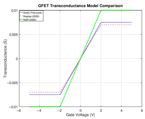
Figure 16.
Comparison of the transconductance behavior of the GFET using three different models (Nastasi and Romano [5], Nastasi [36], and our work).
Figure 17 illustrates the transfer curves of the GFET based on the N&R model [6] and our SimQ model. Both the SimQ and N&R models reproduce the characteristic bell shape typical of the ambipolar behavior in graphene-based field-effect transistors. However, we observe some differences. The SimQ model predicts slightly steeper current peaks and a more abrupt transition between the electron and hole conduction regions, while the N&R model shows a smoother transition and less differentiation between the positive and negative voltage branches.
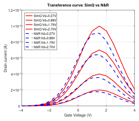
Figure 17.
Comparison of transfer curves of the GFET using two different models.
Figure 18 depicts the output characteristics of the GFET based on the N&R [6] and SimQ models. These models exhibit the typical behavior expected of a field-effect transistor, with an initial rise in current followed by a gradual trend toward saturation. The SimQ curves show a slightly higher current than the N&R ones, particularly at higher drain voltages, and a smoother transition to saturation. These differences probably reflect variations in the treatment of transport phenomena and the interaction between the channel and the contacts in each model.
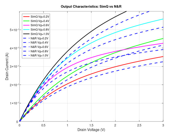
Figure 18.
Comparison of the output characteristic curves of the GFET based on the N&R [6] and SimQ models.
Figure 19 provides a detailed overview of the comparison of transmission probabilities between the SimQ and N&R models. The results show differences in how each model treats transport mechanisms. In the energy range between −1 eV and 1 eV, SimQ predicts noticeably higher Landauer transmission probabilities than N&R, suggesting a higher efficiency in ballistic carrier transport.
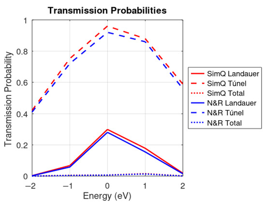
Figure 19.
Transmission probabilities versus energy using SimQ and reference models across energy spectrum (−2 to 2 eV). In the critical region between −1 and 1 eV, SimQ predicts higher Landauer transmission, indicating more efficient ballistic transport. These differences in quantum transport treatment explain observed variations in electrical characteristics between models.
Similarly, the tunneling probabilities are high in the SimQ model, indicating a high permeability of the potential barriers. This difference is particularly relevant because it suggests that SimQ captures the quantum effects in the device with better detail. The observed behavior is consistent with the ambipolar and bandgap-free characteristics of graphene, where carriers can pass through potential barriers with a high probability [2,37]. The comparison of the overall transmission probabilities reflects these differences, showing how the different transport mechanisms combine to determine the overall behavior of the device. These variations in transmission predictions between the two models help explain the observed differences in the electrical characteristics and overall performance of the device [5,6]. The coexistence of Landauer transmission mechanisms (Table 2) suggests an operating regime where both processes contribute significantly to transport. This duality in transport mechanisms explains the observed high conductivity and the ability of the device to operate efficiently across different voltage regimes. The quantitative comparison of the key parameters, summarized in Table 3, shows a remarkable agreement between both models. Mobility, transmission probabilities, quantum capacitance, and cut-off frequencies present differences of less than 8% in all cases, suggesting a strong consistency in the physical description of the device.
On the other hand, Figure 20 shows a comparison of different theoretical models of quantum transmission in GFETs. The SimQ model exhibits transmission maxima at E ∈ [−2, −1] eV and [1, 2] eV with T ≈ 0.42 near E = 0 (see Table 4). The Klein theory [32] (blue dotted line) predicts a sharp minimum at E = 0 due to thermal effects, characteristic of the perfect relativistic tunneling of chiral carriers. A quadratic dependence on energy (T ∝ E2) emerges from the conservation of helicity in graphene. The Allain & Fuchs mode [20] (green dot-dash line) exhibits a maximum at E = 0, highlighting the dominant role of chirality conservation at a finite temperature (300 K). The inclusion of thermal effects via results in qualitatively different behavior compared to the other models. In summary, the comparative analysis shows that the results of the SimQ model agree with the reference models. The observed differences are principally due to variations in the approaches used to capture the quantum and transport phenomena, but they remain within a relatively small range, reinforcing the validity and robustness of the SimQ model presented in this work.
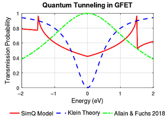
Figure 20.
Transmission probability comparison with Klein theory [34] and Allain & Fuchs model [20], highlighting different approaches to carrier transport in graphene.
Table 4.
Comparative summary of transmission models.
The theoretical models of Klein tunneling [20,34] provide valuable insights into the quantum transport mechanisms in graphene; recent experimental studies have provided crucial validation of these phenomena. Young and Kim [19] demonstrated the direct observation of Klein tunneling in graphene heterojunctions, measuring transmission probabilities that closely matched theoretical predictions. Their experiments showed transmission coefficients of 0.4–0.5 at normal incidence, aligning well with SimQ’s predicted value of ~0.42 near E = 0. Furthermore, experimental work by Stander et al. [16] on graphene p-n junctions reported clear signatures of Klein tunneling, with the measured conductance following the angular dependence predicted by theory. Their results showed transmission probabilities exceeding 0.3 for normal incident carriers, providing strong experimental support for the tunneling mechanisms implemented in our model. Particularly relevant to our work are the high-field transport measurements by Chen et al. [17], who observed mobility values between 3500 and 4000 cm2/V·s at room temperature, remarkably consistent with the SimQ predictions.
Urban et al. [13] demonstrated experimentally that mobility is independent of gate voltage when the contact resistance effect is removed. They showed that mobility values range from 4000 cm2/V·s at low fields to approximately 2000 cm2/V·s at 5 V/μm, with degradation primarily attributed to phonon scattering at temperatures above 250 K. Finally, we compare our mobility results with those reported in other notable works in the field, as shown in Figure 21. This figure reports a direct comparison between the mobility values obtained with SimQ and those reported by Urban et al. [13] and Tian et al. [14] as a function of electric field. All datasets show a decrease in mobility with an increasing field, but with quantitative differences. SimQ predicts a more gradual degradation compared to Urban, maintaining slightly higher mobility values throughout the considered range. Tian’s theoretical model shows more significant mobility degradation at high fields, particularly beyond 3 V/μm.
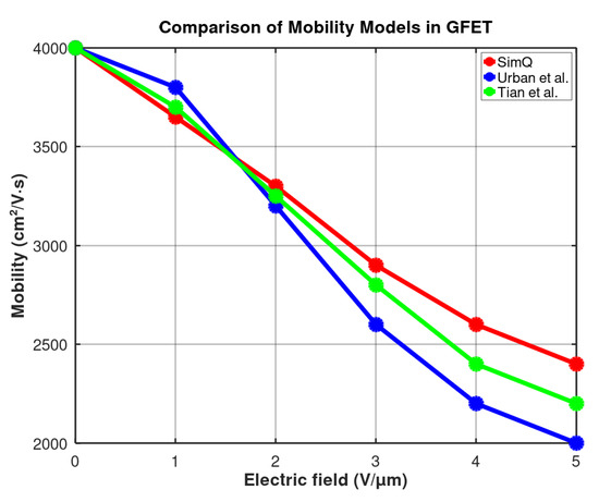
Figure 21.
Mobility comparison with models reported by [13,14] as a function of electric field.
Figure 22 shows the absolute and relative differences in the electric field using the SimQ model, Urban et al. [13], and Tian et al. [14]. The absolute differences (Figure 22a) increase with the electric field. The model of Tian et al. [14] registers maximum differences close to 500 cm2/V·s between 3 and 5 V/μm. On the other hand, the model of Urban et al. [13] exhibits differences around 400 cm2/V·s at high fields. Figure 22b illustrates the relative differences in the electric field from approximately 5% at low electric fields to 20% at higher electric fields for Urban et al. [13]. Tian et al.’s model [14] presents a trend reaching a relative difference of approximately 25% at 5 V/μm.
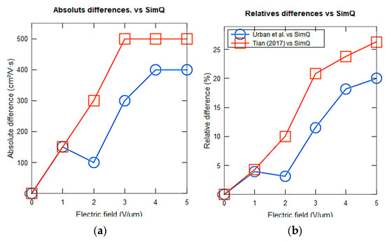
Figure 22.
(a) Absolute difference and (b) relative difference in the electric field using different models of Urban et al. [13] and Tian et al. [14].
Table 3 describes a comparison of the key parameters of the GFET using the SimQ model and the models of Urban et al. [13] and Tian et al. [14]. Our SimQ model agreed well with the results of the models of Urban et al. [13] and Tian et al. [14]. Comparative values were extracted from specific sections of the reference works, as follows: mobility values derived from the contact resistance and sheet resistance data presented by Urban et al. [11] and Tian et al. [14], transmission coefficients from [11,12], quantum capacitance measurements from [11], and cut-off frequency estimations from [12].
The implementation of SimQ in Octave demonstrates a significant computational efficiency while maintaining accuracy in transport calculations. Our performance analysis focused on the following three key aspects: execution time, computational resource utilization, and scalability. We used a standard desktop computer (Lenovo, Beijing, China, Intel i5 processor, 16 GB RAM).
Our SimQ model provides faster execution for basic transport calculations, a lower memory footprint for equivalent simulations, a greater flexibility for customization and modification, and open-source accessibility for academic research. These performance characteristics make SimQ suitable for rapid device prototyping and academic research, where both computational efficiency and flexibility are crucial.
Figure 23 illustrates the computational workflow and optimization strategies implemented in SimQ, showing the key processing stages and their interactions. This modular structure enables efficient resource utilization while maintaining accuracy in quantum transport calculations. Our SimQ model operates under idealized conditions that present important limitations for real-world applications. Future versions of SimQ could incorporate coupled thermal modeling, advanced interface treatment, and additional scattering mechanisms to bridge the gap between simulation and experimental behavior.
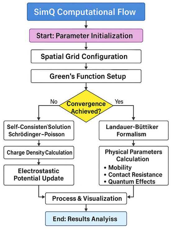
Figure 23.
Flow diagram of a complete simulation process using the SimQ model.
Table 5 provides a comparison of different parameters of GFETs using the SimQ model and GFET Lab [38] and Atlas (Silvaco) [39] models. While commercial tools like ATLAS offer more sophisticated physical models in some areas, SimQ provides multi-technology support capabilities that are not available with other open-source alternatives like GFET Lab or NanoHub tools. This makes SimQ particularly valuable for researchers exploring the effects of fabrication-dependent variations and defects on GFET performance.
Table 5.
Comparison of parameters of GFETs using SimQ with GFET Lab and Atlas simulators.
4. Conclusions
A quantum transport simulation model of GFETs developed using the open-source Ocatave programming language is proposed. This simulation model SimQ uses the Landauer–Büttiker formalism with self-consistent Schrödinger–Poisson solutions. SimQ includes quantum tunneling effects and phonon scattering mechanisms, which enables the reliable prediction of GFET performance in various operating regimes. The proposed simulation model can be employed as technology support for GFETs, particularly regarding fabrication-dependent variations. The results of our simulation model agree well with those of other simulation models reported in the literature. Our simulation model can predict the fundamental electrical characteristics of GFETs, including current–voltage relations, transconductance, carrier mobility, and their dependence on the electric field, contact resistance, and the Ion/Ioff ratio, as well as high-frequency behavior. SimQ offers significant insights into the intrinsic operation of GFETs that might be overlooked with simpler modeling approaches.
Author Contributions
Conceptualization, M.H.-G. and J.M.-C.; methodology, M.H.-G., E.D.-A. and P.J.G.-R.; investigation, P.M.-E., E.D.-A. and J.M.-C.; resources, A.L.H.-M., P.J.G.-R. and J.C.N.-M.; writing—original draft preparation, M.H.-G., P.M.-E. and J.M.-C.; writing—review and editing, E.D.-A. and A.L.H.-M. All authors have read and agreed to the published version of the manuscript.
Funding
This research received no external funding.
Institutional Review Board Statement
Not applicable.
Informed Consent Statement
Not applicable.
Data Availability Statement
The data are contained within the article.
Acknowledgments
We would like to thank to Secretariat of Science, Humanities, Technology and Innovation (SECIHTI) for the scholarship 858971, and to the Program of Doctorate in Materials and Nanoscience in Micro and Nanotechnology Research Center at Universidad Veracruzana, Mexico.
Conflicts of Interest
The authors declare no conflicts of interest.
References
- Novoselov, K.S.; Geim, A.K.; Morozov, S.V.; Jiang, D.; Zhang, Y.; Dubonos, S.V.; Grigorieva, I.V.; Firsov, A.A. Electric Field Effect in Atomically Thin Carbon Films. Science 2004, 306, 666–669. [Google Scholar] [CrossRef]
- Castro Neto, A.H.; Guinea, F.; Peres, N.M.; Novoselov, K.S.; Geim, A.K. The electronic properties of graphene. Rev. Mod. Phys. 2009, 81, 109–162. [Google Scholar] [CrossRef]
- Schwierz, F. Graphene transistors. Nat. Nanotechnol. 2010, 5, 487–496. [Google Scholar] [CrossRef] [PubMed]
- Fiori, G.; Bonaccorso, F.; Iannaccone, G.; Palacios, T.; Neumaier, D.; Seabaugh, A.; Banerjee, K.; Colombo, L. Electronics based on two-dimensional materials. Nat. Nanotechnol. 2014, 9, 768–779. [Google Scholar] [CrossRef] [PubMed]
- Nastasi, G.; Romano, V. An Efficient GFET Structure. IEEE Trans. Electron Devices 2020, 68, 4729–4734. [Google Scholar] [CrossRef]
- Nastasi, G.; Romano, V. Drift-diffusion models for the simulation of a graphene field effect transistor. J. Math. Ind. 2020, 87, 105300. [Google Scholar] [CrossRef]
- Datta, S. Nanoscale device modeling the Green’s function method. Superlattices Microstruct. 2000, 28, 253–278. [Google Scholar] [CrossRef]
- Datta, S. Lessons from Nanoelectronics: B. Quantum Transport; World Scientific Publishing Company: Singapore, 2018. [Google Scholar]
- Peres, N.R. The transport properties of graphene: An introduction. Rev. Mod. Phys. 2010, 82, 2673–2700. [Google Scholar] [CrossRef]
- Das Sarma, S.; Gwang, E.H.; Rossi, E. Electronic transport in two-dimensional graphene. Rev. Mod. Phys. 2011, 83, 407–470. [Google Scholar] [CrossRef]
- Keldysh, L.V. Diagram Technique for nonequilibrium processes. Sov. Phys. JETP 1964, 47, 1515–1527. [Google Scholar] [CrossRef]
- Baym, G.; Kadanoff, L.P. Quantum Statistical Mechanics: Green’s Function Methods in Equilibrium and Nonequi-Librium Problems; CRC Press: Boca Raton, FL, USA, 1962. [Google Scholar]
- Urban, F.; Grzegorz, L.; Grillo, A.; Martucciello, N.; Bartolomeo, D.A. Contact resistance and mobility in back-gate graphene transistors. Nano Express 2020, 1, 010001. [Google Scholar] [CrossRef]
- Tian, J. Theory, Modelling and Implementation of Graphene Field-Effect Transistor. Ph.D. Thesis, Queen Mary University of London, London, UK, 2017. [Google Scholar]
- Ariel, V.; Natan, A. Electron Effective Mass in Graphene. arXiv 2012, arXiv:1206.6100. [Google Scholar] [CrossRef]
- Stander, N.; Huard, B.; Goldhaber-Gordon, D. Evidence for Klein Tunneling in Graphene p-n Junctions. Phys. Rev. Lett. 2009, 102, 1079–7114. [Google Scholar] [CrossRef]
- Chen, S.; Van de Put, M.L.; Fischetti, M.V. Quantum transport simulation of graphene-nanoribbon field-effect transistors with defects. J. Comput. Electron. 2021, 20, 21–37. [Google Scholar] [CrossRef]
- Katsnelson, M.I.; Novoselov, K.S.; Geim, A.K. Chiral tunnelling and the Klein paradox in graphene. Nat. Phys. 2006, 2, 620–625. [Google Scholar] [CrossRef]
- Young, A.F.; Kim, P. Quantum interference and Klein tunnelling in graphene heterojunctions. Nat. Phys. 2009, 5, 222–226. [Google Scholar] [CrossRef]
- Allain, P.E.; Fuchs, J.N. Klein tunneling and electron optics in graphene-based quantum devices. Semicond. Sci. Technol. 2018, 33. [Google Scholar] [CrossRef]
- Jimenez, D.; Moldovan, O. Explicit drain-current model of graphene field-effect transistors targeting analog and radio-frequency applications. IEEE Trans. Electron Devices 2011, 58, 4049–4052. [Google Scholar] [CrossRef]
- Du, C.; Yu, L.; Liu, X.; Liu, L.; Wang, C.-Z. Oscilatory electrostatic potential in graphene induced by IV group. Sci. Rep. 2017, 7, 13152. [Google Scholar] [CrossRef]
- Majorana, A.; Mascali, G.; Romano, V. Charge transport and mobility in monolayer graphene. J. Math. Ind. 2017, 7, 4. [Google Scholar] [CrossRef][Green Version]
- Data, S.; Duncan, T. Quantum Transport. Atom to Transistor; Cambridge University Press: New York, NY, USA, 2005. [Google Scholar]
- Luryi, S. Quantum capacitance devices. Appl. Phys. Lett. 1988, 52, 501–503. [Google Scholar] [CrossRef]
- Fang, T.; Konar, A.; Xing, H.; Jena, D. Carrier statistics and quantum capacitance of graphene sheets and ribbons. Apply. Phys. 2007, 91, 92109. [Google Scholar] [CrossRef]
- Nika, D.L.; Balandin, A.A. Two-dimensional phonon transport in graphene. J. Phys. Condens. Matter 2012, 24, 233203. [Google Scholar] [CrossRef]
- Kubakaddi, S.S. Interaction of massless Dirac electrons with acoustic phonons in graphene at low temperatures. Phys. Rev. B 2009, 79, 075417. [Google Scholar] [CrossRef]
- Li, X.; Barry, E.A.; Zavada, J.M.; Nardelli, M.B.; Kim, K.W. Surface polar phonon dominated electron transport in graphene. Appl. Phys. Lett. 2010, 97, 232105. [Google Scholar] [CrossRef]
- Zhu, W.; PerenveInos, V.; Freitag, M.; Avouris, P. Carrier scattering, mobilities, and electrostatic potential in monolayer, bilayer, and trilayer graphene. Phys. Rev. B 2009, 80, 235402. [Google Scholar] [CrossRef]
- Chen, J.; Jang, C.; Xiao, S.; Ishigami, M.; Fuhrer, M. Intrinsic and extrinsic performance limits of graphene devices on SiO2. Nat. Nanotechnol. 2008, 3, 206–209. [Google Scholar] [CrossRef] [PubMed]
- Ferry, D.R.; Goodnick, S.M.; Bird, J. Transport in Nanostructures, 2nd ed.; Arizona State University: Phoenix, AZ, USA; Universidad Estatal de Nueva York: New York, NY, USA; Cambridge University Press: Buffalo, NY, USA, 2009. [Google Scholar]
- Zhong, H.; Zhang, Z.; Xu, H.; Qiu, C.; Peng, L.-M. Comparison of mobility extraction methods based on field-effect measurements for graphene. AIP Adv. 2015, 5, 057136. [Google Scholar] [CrossRef]
- Klein, O. Die Reflexion von Elektronen an einem Potentialsprung nach der relativistischen Dynamik von Dirac. Physik 1929, 53, 157–165. [Google Scholar] [CrossRef]
- Vaquero, D.; Clericó, V.; Schmitz, M.; Delgado-Notario, J.; Martin, A.; Sánchez, J.; Muller, C.; Rubi, K.; Watanabe, K.; Tanuguchi, T.; et al. Pezzini. Phonon-mediated room-temperature quantum Hall transport in graphene. Nat. Commun. 2023, 14, 318. [Google Scholar] [CrossRef]
- Nastasi, G. Modeling and Simulation of Charge Transport in Graphene. Ph.D. Thesis, University of Catania, Catania, Italy, 2020. [Google Scholar]
- Pandey, D.; Villani, M.; Colomés, E.; Zhen, Z.; Oriols, X. Implications of the Klein tunneling times on high frequency graphene devices using Bohmian trajectories. Semicond. Sci. Technol. 2019, 34, 034002. [Google Scholar] [CrossRef]
- Tye, N.J.; Tadbier, A.W.; Hofmann, S.; Stanley-Marbell, P. GFET Lab: A Graphene Field-Effect Transistor TCAD Tool. arXiv 2022. [Google Scholar] [CrossRef]
- SILVACO International. ATLAS User’s Manual: Device Simulation Software; SILVACO International: Santa Clara, CA, USA, 2023. [Google Scholar]


Disclaimer/Publisher’s Note: The statements, opinions and data contained in all publications are solely those of the individual author(s) and contributor(s) and not of MDPI and/or the editor(s). MDPI and/or the editor(s) disclaim responsibility for any injury to people or property resulting from any ideas, methods, instructions or products referred to in the content. |
© 2025 by the authors. Licensee MDPI, Basel, Switzerland. This article is an open access article distributed under the terms and conditions of the Creative Commons Attribution (CC BY) license (https://creativecommons.org/licenses/by/4.0/).