Article

Design of an Integrated Near-Field Communication and Wireless Power Transfer Coupler for Mobile Device Applications

1
Department of ICT Convergence, Soonchunhyang University, Asan 31538, Republic of Korea
2
Department of Electronic Engineering, Soonchunhyang University, Asan 31538, Republic of Korea
*
Author to whom correspondence should be addressed.
Technologies 2025, 13(5), 207; https://doi.org/10.3390/technologies13050207 (registering DOI)
Submission received: 16 March 2025 / Revised: 18 April 2025 / Accepted: 14 May 2025 / Published: 17 May 2025

Abstract

:
In this study, we propose a model that integrates a near-field communication (NFC) coupler and a wireless power transfer (WPT) coupler for mobile device applications. The NFC and WPT couplers were independently designed and then combined into a four-port NFC–WPT coupler. The proposed practical equivalent circuit (PEC) introduces a novel multi-port network representation, where inductive and capacitive coupling structures are modeled using T-model and Pi-model configurations, respectively. Based on this circuit model, we present a detailed theoretical approach for deriving a 4 × 4 S-parameter matrix by converting the transmission matrices of the partitioned circuit networks into S-parameters. The comparison between the theoretical analysis and the simulation results shows an error of less than 2.4%, which demonstrates the high accuracy of the proposed method.

1. Introduction

Wireless power transfer (WPT) technology enables wireless energy transmission through various methods, including inductive coupling-based inductive wireless power transfer (IPT) and capacitive coupling-based capacitive wireless power transfer (CPT) [1]. This technology has been extensively studied for application in devices requiring a power supply [2,3,4].
The IPT method utilizes a coil structure for inductive coupling, whereas the CPT method employs a metal plate structure for capacitive coupling. The IPT achieves high power transfer efficiency through strong magnetic coupling at close range; however, when metal plates are nearby, eddy currents are induced, leading to magnetic field distortion and variations in electrical characteristics such as the magnetic coupling coefficient and self-inductance [5]. Additionally, its effects on other devices and human exposure cannot be ignored [6,7]. In contrast, CPT is free from these issues [8], but it has limitations in terms of frequency characteristics and restrictions on the density of the electric field, which is the primary medium for energy transfer [1].
On the other hand, there is a near-field communication (NFC) system that utilizes the principles of WPT. It is an essential technology incorporated into mobile devices for short-range communication. NFC employs a coil-based magnetic resonance method to transfer power and transmit data at 13.56 MHz. Therefore, its power transfer mechanism is fundamentally similar to that of IPT. Since both WPT and NFC technologies must be integrated into a single device, research is being conducted to design systems with efficient structures [9,10].
There are two main approaches to integrating WPT and NFC; one method involves using a single coil for both technologies [11], while the other approach designs a single coil to support both WPT and NFC operations simultaneously [12]. However, such methods are highly sensitive to impedance variations and struggle to meet the wide bandwidth required by NFC, making simultaneous implementation challenging. Additionally, a fundamental limitation is that WPT and NFC cannot operate simultaneously on a single coil. Therefore, an alternative approach is to design WPT and NFC couplers independently and then combine them [13,14,15].
Previous research has explored hybrid structures by integrating NFC antennas with metal covers for smartphone applications [15]. In this design, the metal cover is utilized as a CPT coupler, while the NFC coil functions as an IPT coupler, following the principle of mixed-coupling wireless power transfer. However, this method is also unable to achieve simultaneous activation of both NFC and WPT in practical applications.
Therefore, as illustrated in Figure 1, designing WPT and NFC separately so that the transmitter and receiver of each system have distinct ports can potentially overcome the limitations of simultaneous activation. However, analyzing the coupling effects of couplers, including this approach, is a crucial step. In multi-port analysis, impedance matching circuits are typically not applied, eliminating the need for complex equivalent circuit model analysis [16,17,18,19,20,21]. Nevertheless, when additional circuits are introduced, a partitional circuit network (PCN) becomes essential to enable precise theoretical design.
Conventional coupling methods are typically configured as two-port networks, making it challenging to analyze mutual coupling factors, as they primarily rely on evaluating the overall impedance of the coupler. However, by developing a PCN for theoretical design, it is possible to accurately analyze the coupling effects and losses between couplers.
In this study, we propose a theoretical design for an NFC with a WPT coupler, which combines an NFC coupler resonating at 13.56 MHz with a WPT coupler resonating at 6.78 MHz. The integrated WPT system incorporates both IPT and CPT couplers. A practical equivalent circuit (PEC) model, including coupler loss resistance, is developed and validated by comparing it with 3D full-wave simulation results.
The PEC is formulated using a T-model to represent the transmission matrix, while the NFC coupler incorporates a ferrite material to examine the effects of magnetic interference. A high-efficiency coupler is designed to demonstrate its suitability for mobile device applications.
The key contributions of this study can be summarized as follows:
  • An equivalent circuit model is proposed, in which all self and mutual coupling elements in a multi-port network are represented using unified T-model and Pi-model structures. This contrasts with conventional methods that describe each port independently, without fully expressing inter-port coupling.
  • A formalized theoretical formulation is presented for converting the transmission matrix of the PCN in the practical equivalent circuit model of the NFC–IPT and NFC–CPT couplers into S-parameters.

2. Models of NFC–WPT Coupler

2.1. Theoretical Deisgn Method of PEC Circuit

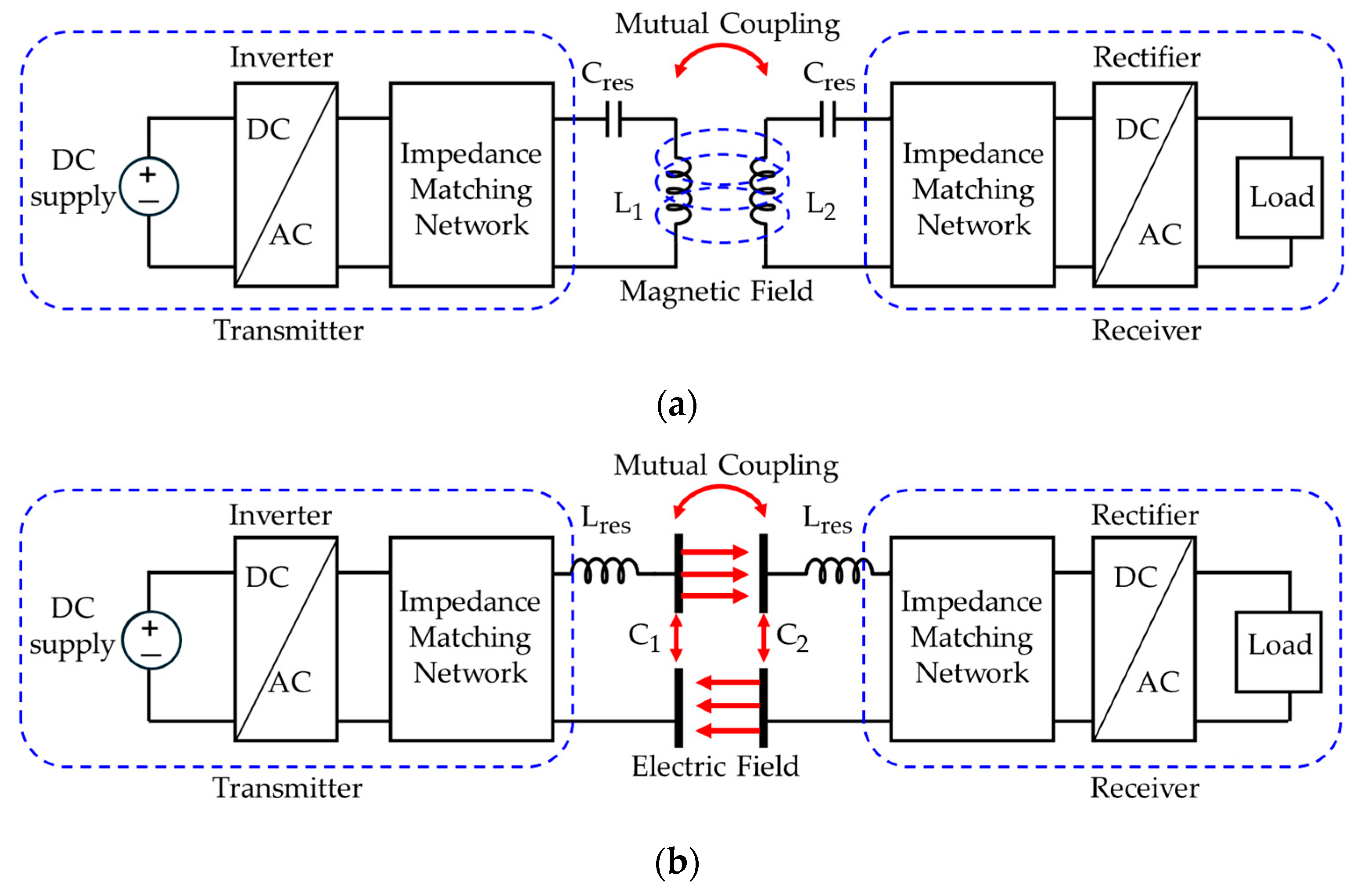
The configurations of the inductive power transfer (IPT) system, based on magnetic field coupling, and the capacitive power transfer (CPT) system, based on electric field coupling, are shown in Figure 2. In Figure 2a, an AC voltage source generates magnetic coupling between two coils, enabling power transfer in the IPT system. In contrast, in Figure 2b, an AC voltage source generates electric coupling between four metal plates, facilitating power transfer in the CPT system.
For these couplers, precise design of the impedance matching circuits for both the transmitter and receiver is essential to maximize coupling at the resonant frequency. In general, the term ‘coupler’ refers to a structure that includes the impedance matching circuit, resonant elements, and primary coupling components, such as coils or metal plates. Accurate equivalent circuit design and analysis at the coupler level are crucial, as they enable the quantification of interference and losses in system design through equivalent circuit parameters.
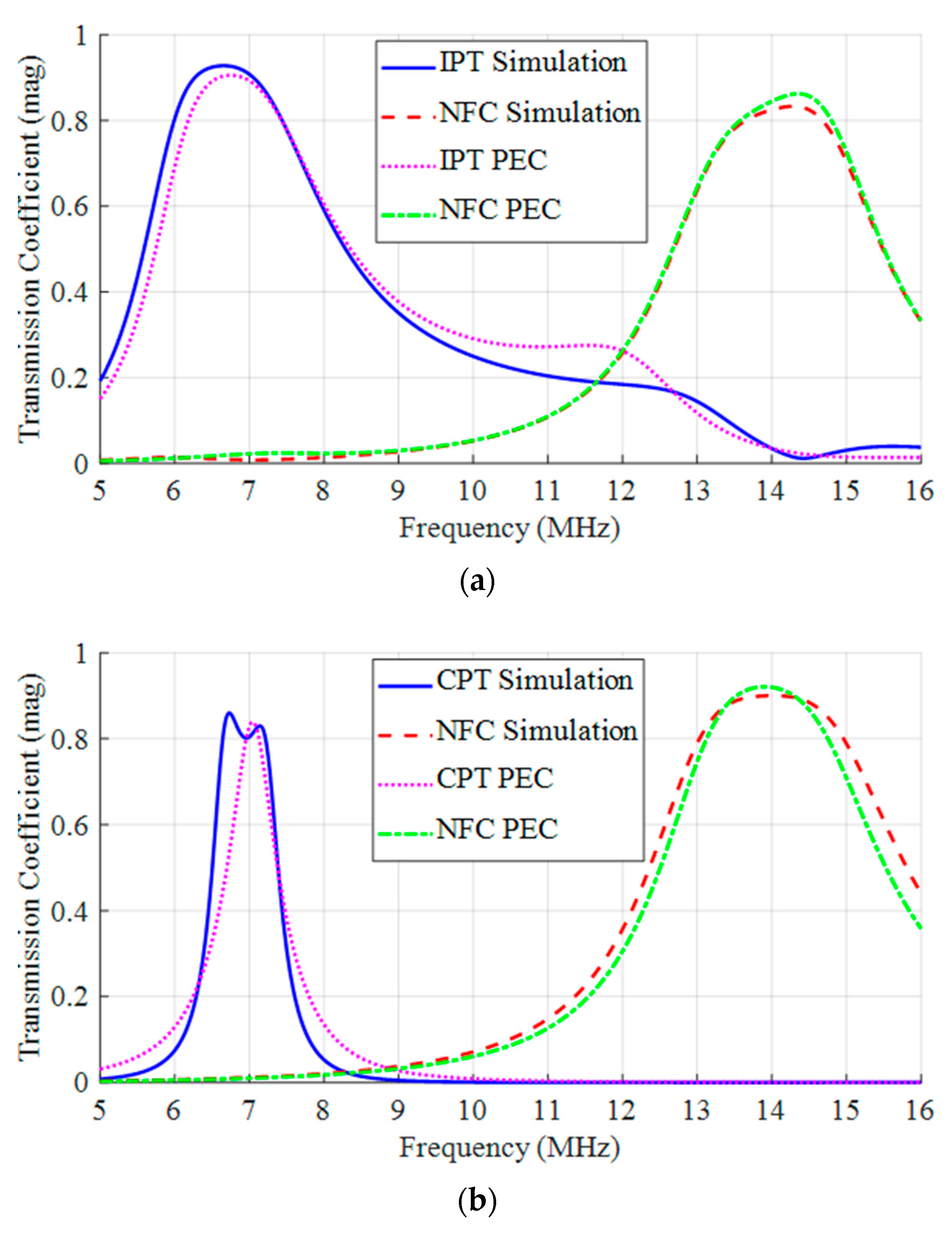
Therefore, a PEC for a four-port network incorporating loss resistance is designed for the NFC–IPT and NFC–CPT hybrid coupler model, and its S-parameters are calculated. Furthermore, previous studies have demonstrated that theoretical analysis based on the equivalent circuit model and electromagnetic simulation results exhibit high agreement with experimental validation [22]. Based on these findings, this study focuses on validating the PEC-based theoretical analysis by comparing it with electromagnetic simulation results obtained using ANSYS HFSS 2021R2, excluding experimental verification.
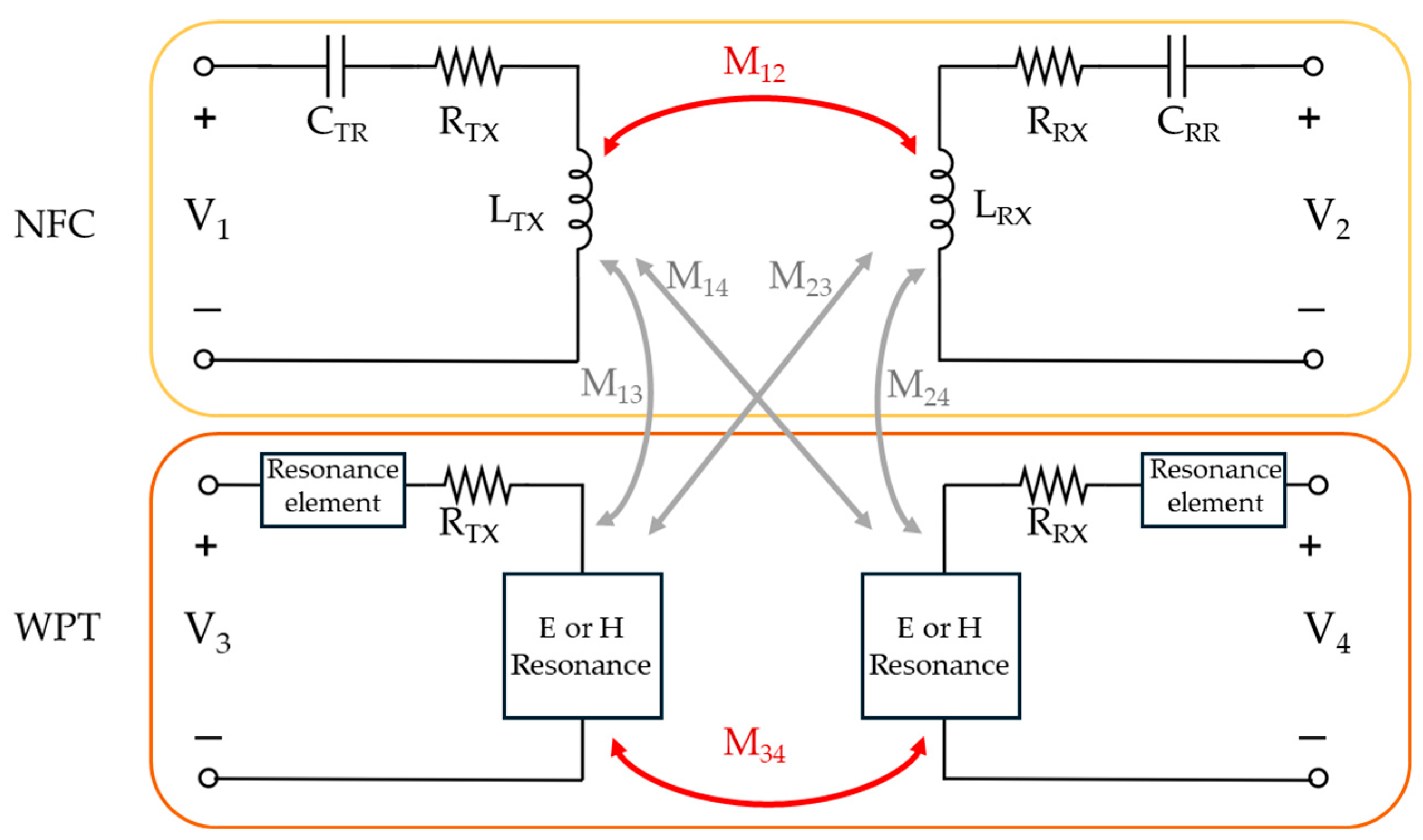
Figure 3 illustrates the link structure of the four-port coupler combining NFC and WPT. The WPT system can be implemented using either IPT or CPT and follows the MIMO WPT link principle [23]. In the NFC coupler, V1 and V3 represent the source voltages of NFC and WPT, respectively, while V2 and V4 correspond to the load voltages.
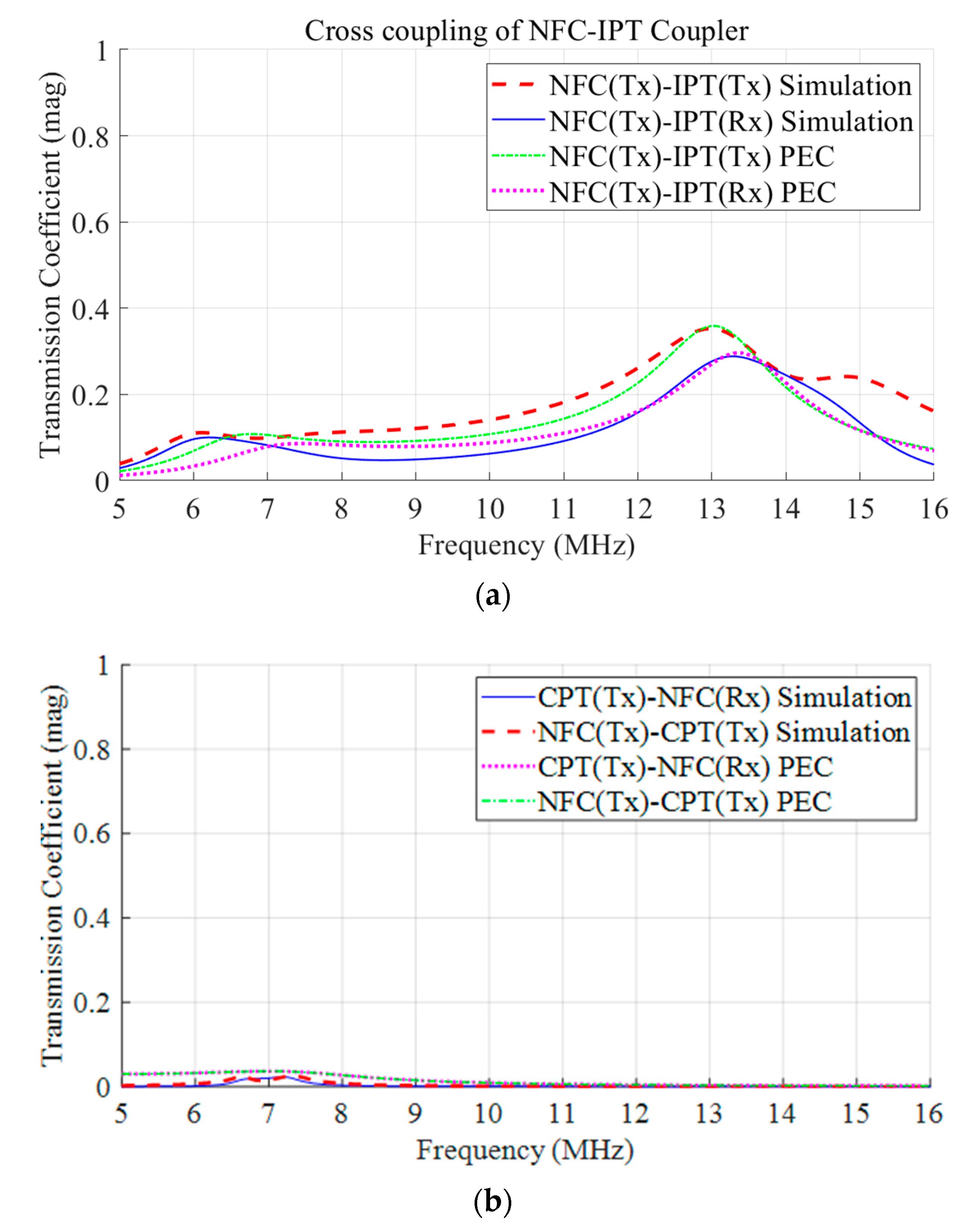
Since the four-port network has a total of six mutual terms, it consists of two main coupling terms and four cross-coupling terms. The main coupling in the NFC coupler is denoted as M12, while that in the WPT coupler is represented as M34. When the WPT system coupled with NFC operates in CPT mode, the resonant fields differ, meaning the cross-coupling terms M13, M14, M23, and M24 can be assumed to be nearly zero. Conversely, when the IPT coupler is applied, magnetic coupling occurs, potentially leading to cross-coupling with the NFC coupler. The equivalent circuit model proposed in this study explicitly represents this coupling effect.
In this study, the PEC of each coupler is theoretically designed and compared with 3D full-wave simulation results. Since the NFC and WPT couplers are combined, a 4 × 4 transmission matrix is derived for four-port network analysis, and the overall S-parameters are calculated. The PEC is structured by segmenting the PCN and defining the transmission matrix for each segment. By converting and multiplying the transmission matrices of each segment into S-parameters, the overall S-parameters of the coupler can be obtained.
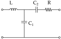
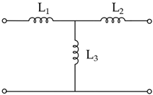
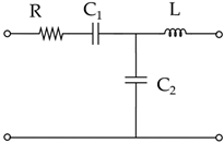
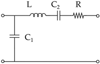
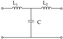
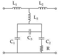
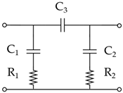
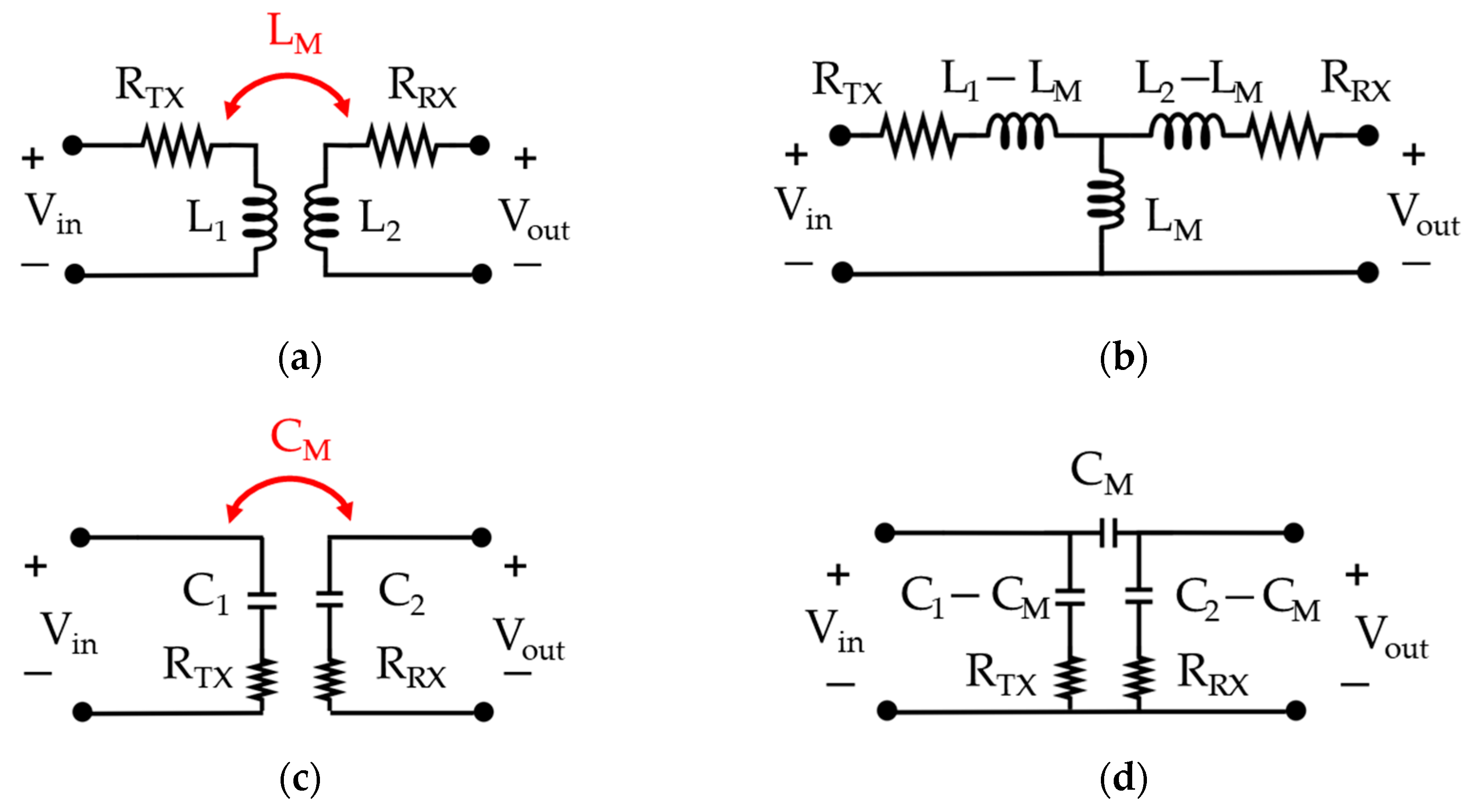
The structure of the PEC matrix varies depending on the coupling field and the matching circuit configuration of the coupler. In this study, the PEC matrix is classified into two types. Since IPT operates via magnetic coupling, the equivalent circuit of Figure 4a can be transformed into a T-model, as shown in Figure 4b, incorporating mutual terms. Meanwhile, the four-plate CPT coupler utilizes electric field coupling, and its equivalent circuit can be transformed from the structure in Figure 4c into a pi-model, as illustrated in Figure 4d. Additionally, all PEC models incorporate coupler loss resistance to ensure high accuracy in comparison with simulation results.
In the equivalent circuits of the two couplers proposed in this study, the PCNs exhibit several common structural patterns. Due to the redundancy in the transmission matrix formulations across all circuit networks, different types of networks are classified. The PCNs of the couplers are categorized accordingly, allowing each to be substituted into the corresponding transmission matrix equation for calculation.

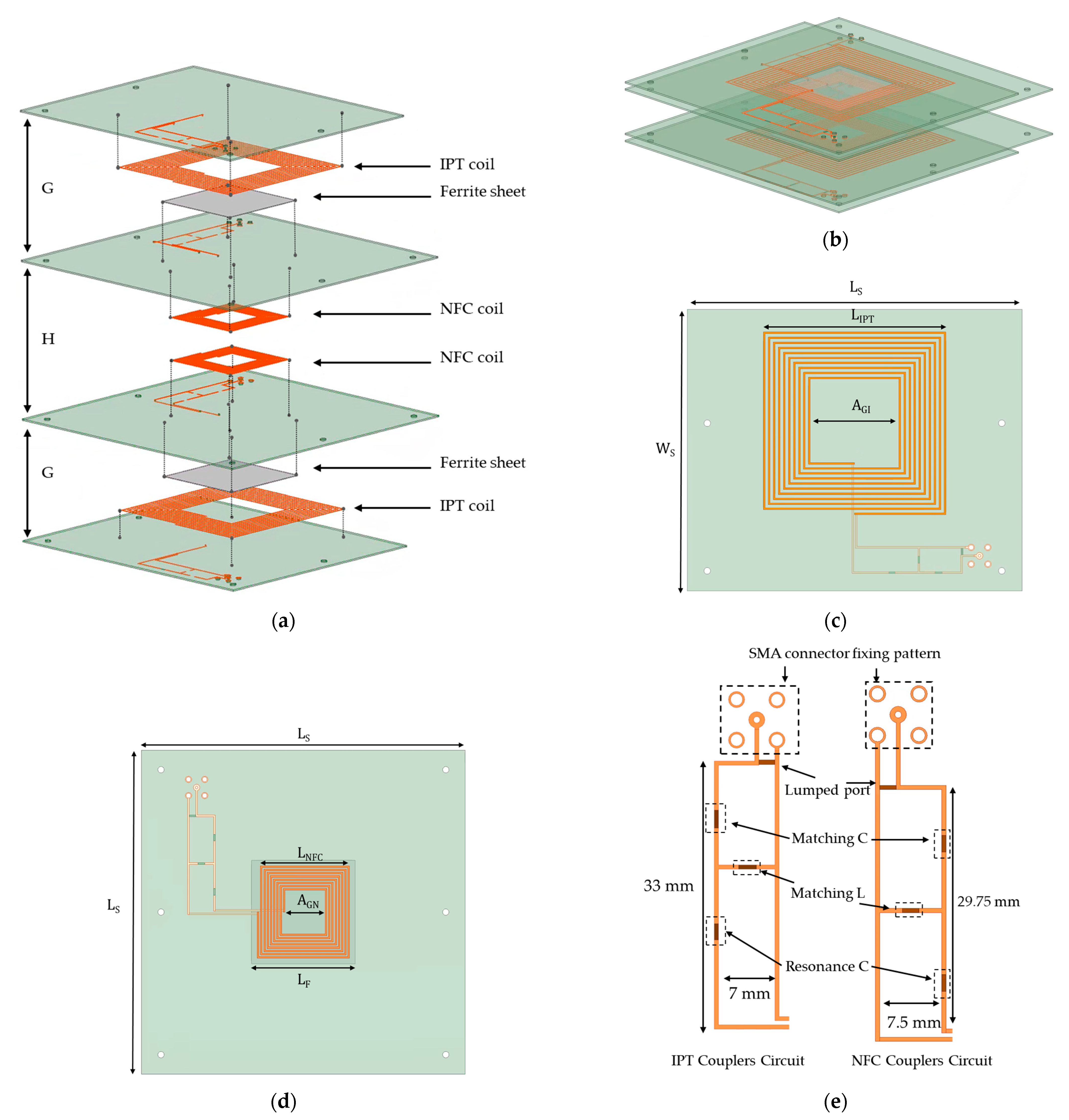
2.2. PEC Model of NFC–IPT

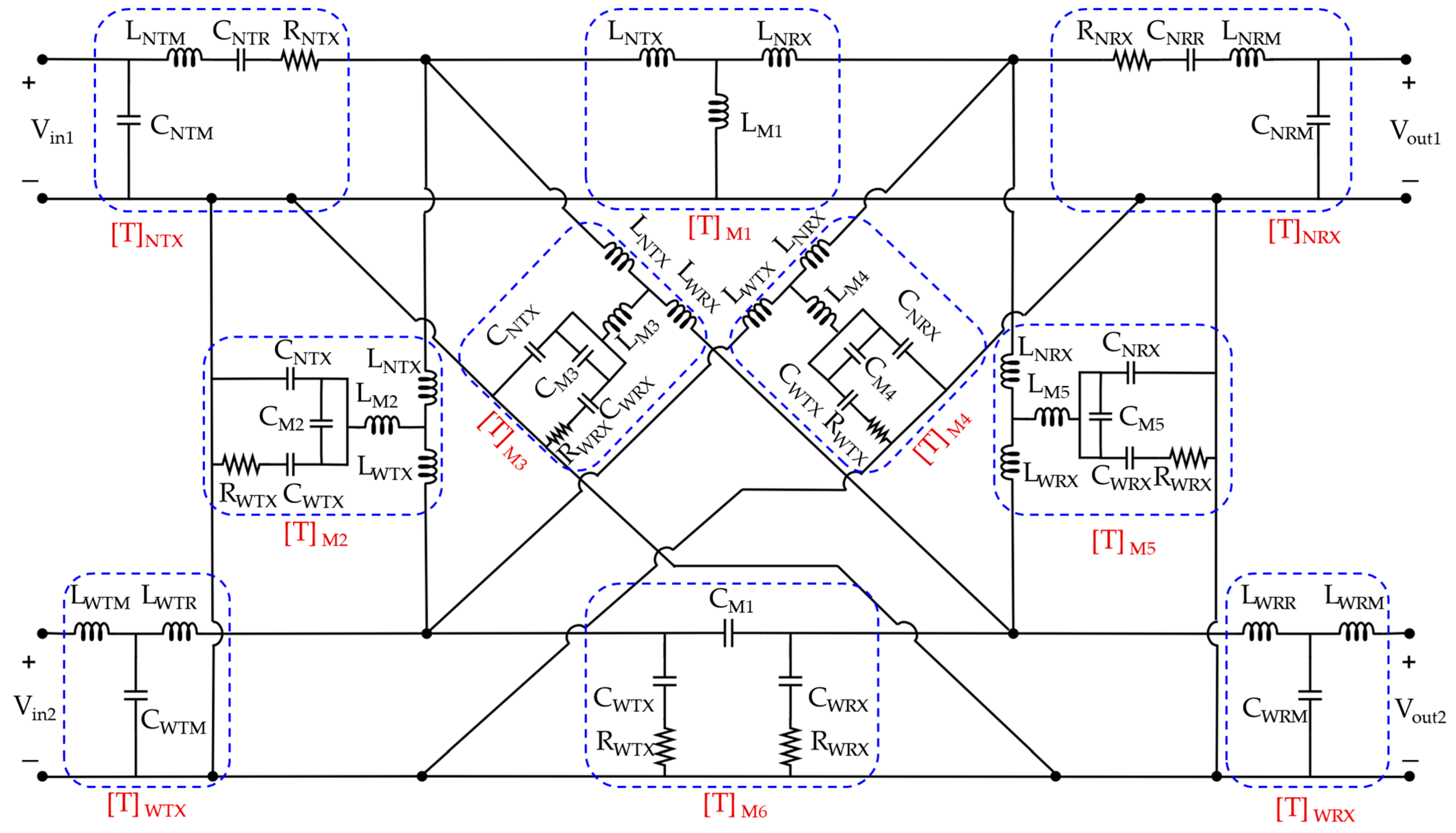
Figure 5 illustrates the four-port network equivalent circuit model combining NFC and IPT couplers. Since coupling occurs between coils, self-inductance and mutual inductance are represented using a T-model circuit. In the four-coil system, six mutual inductance components can be defined and are denoted as LM1 to LM6 in the equivalent circuit model. For example, the mutual inductance between the NFC transmitter and the IPT receiver is represented as LM5.
The impedance matching circuits and resonant capacitors in the NFC transmitter and receiver, along with the inherent loss resistance of the coupler, are represented as [T]NTX and [T]NRX. The circuit network including the self-inductance and mutual inductance of the NFC transmitter and receiver is denoted as [T]M1. Similarly, the circuit network representing the self-inductance and mutual inductance in the coupling between the NFC transmitter and the IPT coupler is expressed as [T]M2.
The 4 × 4 S-parameters of the four-port network can be defined as a combination of 2 × 2 matrices obtained by decomposing Figure 5 into two-port network representations. The S-parameters of the PCNs calculated and multiplied to define the S-parameters of the two-port network as follows.
S T O T A L = S 11 S 12 S 21 S 22 S 13 S 14 S 23 S 24 S 31 S 32 S 41 S 42 S 33 S 34 S 43 S 44
S 11 S 12 S 21 S 22 = S N T X · S M 1 · S N R X S 11 S 13 S 31 S 33 = S N T X · S M 2 · S W T X S 11 S 14 S 41 S 44 = S N T X · S M 5 · S W R X S 22 S 23 S 32 S 33 = S N R X · S M 6 · S W R X S 22 S 24 S 42 S 44 = S N R X · S M 4 · S W R X S 33 S 34 S 43 S 44 = S W T X · S M 3 · S W R X
The parameters illustrated in Figure 5 are summarized in Table 1. To accurately represent self-inductance in the T-model circuit, it must be considered as the value obtained after subtracting mutual inductance, as shown in Figure 4b. In a four-port network, each self-inductance accounts for three mutual inductances.
The PCNs of the NFC–IPT coupled system can be classified into Type A, Type B, and Type C, as summarized in Table 2. Each classification corresponds to a specific circuit configuration, allowing for a systematic analysis of the coupler’s PCN.
For an N-port network’s T-model equivalent circuit, self-inductance (LC) and mutual inductance (M1j) can be conceptually defined as shown in Equation (3). The self-inductance values listed in the table represent ideal values that do not account for the mutual inductance between NFC and IPT. This relationship is incorporated into the S-parameter calculation process of the equivalent circuit model.
L C = L s e l f j = N M 1 j
Using the transmission matrix conversion formulas for each circuit type in the table, the equation can be expressed as follows.
T T y p e A = 1 ω 2 L C 1                     1 j ω C 2 + R 1 ω 2 L C 1 + j ω L j ω C 1                                           1 + C 1 C 2 + j ω C 1 R T T y p e B = 1 L 1 L 3                                     j ω L 1 + L 2 1 + L 1 L 3 1 j ω L 3                                     1 + L 2 L 3 T T y p e C = 1 + C 2 C 1 + j ω C 2 R             1 j ω C 1 + R 1 ω 2 L C 2 + j ω L j ω C 2                                                       1 ω 2 L C 2
To convert the transmission matrix into S-parameters, ref. [24] proposed a method to simplify the complex equations through substitution. By defining the elements of the above matrix as t, the components of the S-parameters can be organized as shown in Table 3. Each term is derived from equations used for substitution, and the S-parameters can be obtained by referring to Equation (5) of the referenced study.

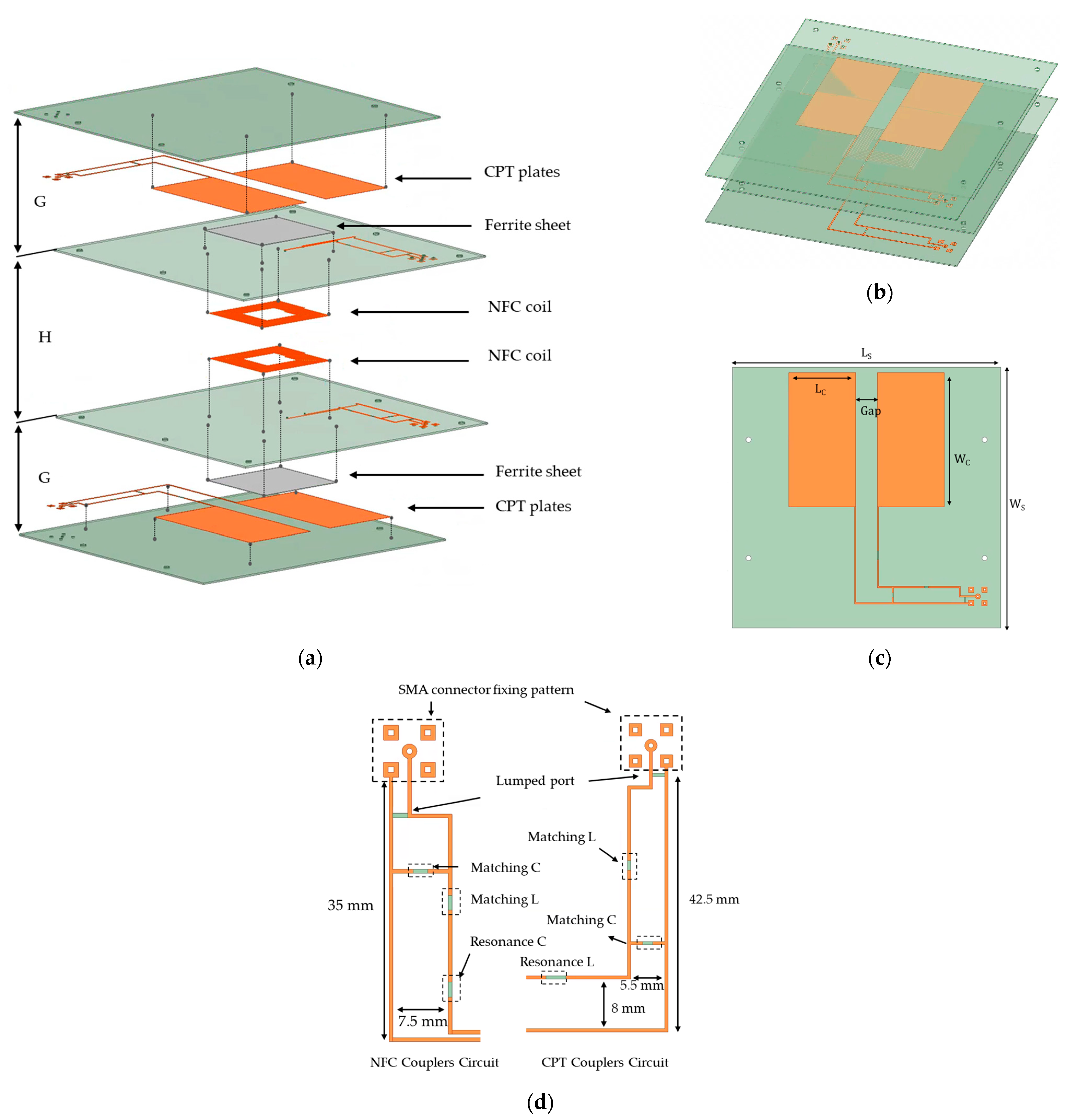
2.3. PEC Model of NFC–CPT

Figure 6 illustrates the four-port network equivalent circuit model combining NFC and CPT couplers. The detailed parameters are summarized in Table 4. Since the NFC transmitter and receiver are coupled through coils, self-inductance and mutual inductance can be represented using a T-model circuit. However, when the NFC transmitter is coupled with the CPT transmitter or receiver, the interaction between coils and metal plates must be considered. The coupling strength between magnetic and electric field components is generally close to zero.
Therefore, in the equivalent circuit model, the matrices for the circuit networks corresponding to [T]M2 through [T]M5 are not explicitly defined but are calculated accordingly. Additionally, the CPT coupler’s self-capacitance, mutual capacitance, and coupler loss resistance are included in a separate network, denoted as [T]M6.
Similar to the NFC–IPT coupler, the 4 × 4 S-parameters can be derived by defining the S-parameters of the two-port networks as follows. While the equivalent circuit model and calculation equations remain the same as those for the NFC–IPT coupler, it is important to note that the numbering of the coupled networks differs.
S 11 S 12 S 21 S 22 = S N T X · S M 1 · S N R X S 11 S 13 S 31 S 33 = S N T X · S M 2 · S W T X S 11 S 14 S 41 S 44 = S N T X · S M 3 · S W R X S 22 S 23 S 32 S 33 = S N R X · S M 4 · S W R X S 22 S 24 S 42 S 44 = S N R X · S M 5 · S W R X S 33 S 34 S 43 S 44 = S W T X · S M 6 · S W R X
The PCNs of the NFC and CPT combined coupler can be classified into Type D, Type E, Type F, and Type G, as shown in Table 5. Each classification corresponds to a specific circuit configuration, allowing for an analysis of the coupler’s PCN. Among them, Type F, which is an uncommon configuration, can be calculated as the sum of Type B and Type G. Type F represents a circuit designed to simultaneously express self-inductance and self-capacitance in the coupling between coils and metal plates. This circuit can be referenced in studies on hybrid wireless power transfer couplers that combine IPT and CPT designs [25].
Since the coupler’s loss resistance of the coil has already been considered in the impedance matching circuit network, only the loss resistance of the CPT coupler is included in Type F. Therefore, the self-capacitance and loss resistance, which are expressed in series, are represented only on the CPT side.
The transmission matrices of the partitioned circuit networks for each Type in Table 5 are as follows.
T T y p e D = 1 j ω L + 1 j ω C 2 + R j ω C 1       C 1 1 C 2 j ω R ω 2 L T T y p e E = 1 ω 2 L 1 C j ω L 1 + L 2 1 ω 2 L 1 C j ω C 1 ω 2 L 2 C T T y p e F = 2 + C 2 C 3 + 1 j ω C 3 R L 1 L 3 1 j ω C 3 +   j ω L 1 + L 2 1 + L 1 L 3 j ω C 2 + 1 R 1 + C 2 C 3 + j ω C 1 + 1 R + 1 j ω L 3 2 + C 1 C 3 + L 2 L 3 [ T ] T y p e G = 1 + C 2 C 3 + 1 j ω C 3 R 1 j ω C 3 j ω C 2 + 1 R 2 1 + C 1 C 3 + 1 j ω C 3 R 1 + j ω C 1 + 1 R 1 + C 1 C 3 + 1 j ω C 3 R
Similar to the NFC–IPT coupler, the S-parameters of the partitioned circuit in the NFC–CPT coupler are shown in Table 6.

3. Simulation Models

3.1. NFC–IPT Coupler

In the simulation model, the substrate on which the copper sheets are placed is Taconic RF-35™ with a dielectric layer. The substrate has a thickness of 0.5 mm, the copper sheet thickness is 0.035 mm, the dielectric constant is 3.5 at 1.9 GHz, and the dielectric loss tangent is 0.0018.
Figure 7a illustrates the coupling structure of the NFC–IPT coupler, where each component is shown separately for clarity. The model replicates a configuration in which coil structures are printed on one side of four substrates. The NFC coupler is stacked between IPT couplers, which are also arranged in a stacked structure. Ferrite material is applied to minimize interference caused by the magnetic field of the coils.
Figure 7b presents the final assembled model based on the coupling method shown in Figure 7a. Figure 7c,d display the top views of the standalone IPT and NFC couplers, respectively. Additionally, the coupler includes circuit traces that incorporate resonant elements, impedance matching circuits, and ports. To implement the SMA connector interface for actual measurements, the model is designed as shown in Figure 7e. Detailed specifications of the coupler can be found in Table 7, referencing the figures.

3.2. NFC–CPT Coupler

The NFC–CPT simulation model is designed using the same RF-35™ substrate as the NFC–IPT model. Figure 8a illustrates the coupling structure of the NFC–CPT coupler, where each component is shown separately for clarity. The model replicates a configuration in which coil structures are printed on one side of four substrates. The NFC coupler is stacked between the IPT couplers, which are also arranged in a stacked structure. Ferrite material is applied to minimize interference caused by the magnetic field of the coils.
Figure 8b presents the final assembled model based on the coupling method shown in Figure 8a. Figure 8c shows the top view of the CPT coupler. The NFC coupler combined with CPT has the same specifications as the NFC coupler combined with IPT, as described earlier. The circuit implementation for the NFC–CPT coupler follows the same approach as the NFC–IPT model and is designed as shown in Figure 8d. Detailed specifications of the coupler can be found in Table 8, referencing the figures.

4. Results and Discussion

A coupler structure with four ports was designed by combining NFC and WPT couplers. As a result, six mutual coupling components are generated. Among them, primary coupling occurs between couplers that exhibit frequency-selective characteristics corresponding to their respective resonant frequencies. The WPT system, which resonates at 6.78 MHz, and the NFC system, which resonates at 13.56 MHz, exhibit precise frequency-selective characteristics. Therefore, it is necessary to observe the transmission coefficients between the NFC transmitter/receiver and the WPT transmitter/receiver, as well as the effects of other coupling interactions.
Figure 9 presents the transmission coefficients of the NFC–IPT coupler and the NFC–CPT coupler. The maximum transmission coefficient of the IPT coupler is 0.93 in the simulation and 0.9 in the PEC model. The maximum transmission coefficient of the NFC coupler is 0.83 in the simulation and 0.86 in the PEC model. The maximum transmission coefficient of the CPT coupler is 0.86 in the simulation and 0.84 in the PEC model. The maximum transmission coefficient of the NFC coupler is 0.9 in the simulation and 0.92 in the PEC model.
When comparing the maximum values of the PEC model analysis and the simulation results, the error rate was within 2.4%. The overall trends in the graphs exhibit similar characteristics.
Figure 10 presents the transmission characteristics of cross-coupling components in NFC–IPT and NFC–CPT couplers. Figure 10a illustrates the coupling between the NFC transmitter and the IPT receiver, as well as between the NFC transmitter and the IPT transmitter. In the 6–7 MHz range, the transmission coefficient for the coupling between the NFC transmitter and the IPT receiver reached a maximum of 0.1 in the simulation and 0.07 in the PEC analysis. Additionally, harmonic components were observed in the cross-coupling. Since 13.56 MHz is an integer multiple of 6.78 MHz, coupling increases when the resonance conditions overlap. Because both NFC and IPT couplers transfer power through inductive coupling, the extent of cross-coupling was significantly high. In contrast, for the NFC–CPT coupler, the transmission coefficient for cross-coupling had a maximum value of 0.03 in the PEC analysis, which is negligible.
The reason why the cross-coupling between the CPT and NFC components is negligible is that the primary energy transfer mechanism in CPT is based on electric fields, whereas NFC operates using magnetic fields. In contrast, in the case of the NFC–IPT coupler, both systems rely on magnetic coupling for energy transfer, which can result in a non-negligible level of cross-coupling.
There are various methods for defining self-inductance in a four-port network to represent the T-model. The key aspect is to accurately determine the inherent self-inductance of the coupler and appropriately compute the mutual inductance according to the equivalent circuit modeling approach.

5. Conclusions

In this study, a hybrid coupler combining NFC and WPT couplers was proposed. Two types of hybrid couplers were designed: NFC–IPT, which combines NFC with IPT, and NFC–CPT, which combines NFC with CPT. A four-port network PEC model was provided for the coupled system, where each coupler has both a transmitter and a receiver.
To theoretically analyze the PEC model, the circuit structures of individual sub-networks were categorized, and the transmission matrices and S-parameters were systematically formulated. By converting the transmission matrices of the sub-networks into S-parameters, a 4 × 4 S-parameter matrix was constructed. The results obtained from this theoretical analysis were compared with 3D full-wave simulation results, demonstrating a high level of agreement.
As a result, both NFC–IPT and NFC–CPT couplers achieved high transmission coefficients. Furthermore, the self-inductance and mutual inductance in the T-model, which are difficult to define in a four-port network, were derived. These findings are expected to contribute to the development of wireless power transfer systems for future applications in mobile devices.

Author Contributions

Conceptualization, S.P. and H.B.; methodology, S.P.; software, H.B.; validation, H.B.; formal analysis, H.B.; investigation, H.B.; resources, S.P.; data curation, H.B.; writing—original draft preparation, H.B.; writing—review and editing, H.B.; visualization, H.B.; supervision, S.P.; project administration, S.P.; funding acquisition, S.P. All authors have read and agreed to the published version of the manuscript.

Funding

This work was supported by the Soonchunhyang University Research Fund.

Institutional Review Board Statement

Not applicable.

Informed Consent Statement

Not applicable.

Data Availability Statement

The raw data supporting the conclusions of this article will be made available by the authors upon request.

Conflicts of Interest

The authors declare no conflicts of interest.

References

  1. Lin, C.-H.; Amir, M.; Tariq, M.; Shahvez, M.; Alamri, B.; Alahmadi, A.; Siddiqui, M.; Beig, A. Comprehensive Analysis of IPT v/s CPT for Wireless EV Charging and Effect of Capacitor Plate Shape and Foreign Particle on CPT. Processes 2021, 9, 1619. [Google Scholar] [CrossRef]
  2. Azad, A.; Tavakoli, R.; Pratik, U.; Varghese, B.; Coopmans, C.; Pantic, Z. A Smart Autonomous WPT System for Electric Wheelchair Applications With Free-Positioning Charging Feature. IEEE J. Emerg. Sel. Topics Power Electron. 2020, 8, 3516–3532. [Google Scholar] [CrossRef]
  3. Huh, J.; Lee, S.W.; Lee, W.Y.; Cho, G.H.; Rim, C.T. Narrow-Width Inductive Power Transfer System for Online Electrical Vehicles. IEEE Trans. Power Electron. 2011, 26, 3666–3679. [Google Scholar] [CrossRef]
  4. Choi, K.W.; Aziz, A.A.; Setiawan, D.; Tran, N.M.; Ginting, L.; Kim, D.I. Distributed Wireless Power Transfer System for Internet of Things Devices. IEEE Internet Things J. 2018, 5, 2657–2671. [Google Scholar] [CrossRef]
  5. Lu, J.; Zhu, G.; Mi, C.C. Foreign Object Detection in Wireless Power Transfer Systems. IEEE Trans. Ind. Applicat. 2022, 58, 1340–1354. [Google Scholar] [CrossRef]
  6. Graham, D.J.; Neasham, J.A.; Sharif, B.S. Investigation of Methods for Data Communication and Power Delivery Through Metals. IEEE Trans. Ind. Electron. 2011, 58, 4972–4980. [Google Scholar] [CrossRef]
  7. Imoru, O.; Jassal, A.; Polinder, H.; Nieuwkoop, E.; Tsado, J.; Jimoh, A.A. An Inductive Power Transfer through Metal Object. In Proceedings of the 2013 1st International Future Energy Electronics Conference (IFEEC), Tainan, Taiwan, 3–6 November 2013; IEEE: New York, NY, USA, 2013; pp. 246–251. [Google Scholar] [CrossRef]
  8. Liu, C.; Hu, A.P. Steady State Analysis of a Capacitively Coupled Contactless Power Transfer System. In Proceedings of the 2009 IEEE Energy Conversion Congress and Exposition, San Jose, CA, USA, 20–24 September 2009; IEEE: New York, NY, USA, 2009; pp. 3233–3238. [Google Scholar] [CrossRef]
  9. Fischbacher, R.; Lopera, J.R.; Pommerenke, D.; Prestros, R.; Auinger, B.; Bösch, W.; Grosinger, J. WPT and NFC Interoperability for Wearables with Miniaturized Coils. In Proceedings of the 2023 IEEE 13th International Conference on RFID Technology and Applications (RFID-TA), Aveiro, Portugal, 4–6 September 2023; IEEE: New York, NY, USA, 2023; pp. 33–36. [Google Scholar] [CrossRef]
  10. Shibuya, H.; Tsukuda, T.; Suzuki, H.; Shimizu, T.; Dobashi, M.; Nishizono, S.; Baba, M.; Sasaki, H.; Terajima, K. A Wireless Charging and Near-Field Communication Combination Module for Mobile Applications. In Proceedings of the 2014 IEEE 64th Electronic Components and Technology Conference (ECTC), Orlando, FL, USA, 27–30 May 2014; IEEE: New York, NY, USA, 2014; pp. 763–768. [Google Scholar] [CrossRef]
  11. Cairo, J.I.; Bonache, J.; Paredes, F.; Martin, F. Reconfigurable System for Wireless Power Transfer (WPT) and Near Field Communications (NFC). IEEE J. Radio Freq. Identif. 2017, 1, 253–259. [Google Scholar] [CrossRef]
  12. Huang, Q.; Ma, Z.; Wang, S.; Yang, Y. Integration of Near-Field Communication (NFC) Antenna and Wireless Charging Coil for Portable Electronic Products. IEEE J. Emerg. Sel. Top. Power Electron. 2024, 12, 3415–3425. [Google Scholar] [CrossRef]
  13. Fischbacher, R.; Lopera, J.R.; Pommerenke, D.; Prestros, R.; Auinger, B.; Bösch, W.; Grosinger, J. Communication Quality Analysis for WPT and NFC Systems via Broadband Equivalent Circuit Models. Antennas Wirel. Propag. Lett. 2024, 23, 4–8. [Google Scholar] [CrossRef]
  14. Fischbacher, R.; Gortschacher, L.; Merlin, E.; Muhlmann, U.; Amtmann, F.; Priller, P.; Bosch, W.; Grosinger, J. EC Model for WPT and NFC Systems Interoperability Analysis. In Proceedings of the 2021 IEEE Radio and Wireless Symposium (RWS), San Diego, CA, USA, 17–22 January 2021; IEEE: New York, NY, USA, 2021; pp. 112–115. [Google Scholar] [CrossRef]
  15. Zhu, J.-Q.; Ban, Y.-L.; Xu, R.-M.; Mi, C.C. An NFC-Connected Coupler Using IPT-CPT-Combined Wireless Charging for Metal-Cover Smartphone Applications. IEEE Trans. Power Electron. 2021, 36, 6323–6338. [Google Scholar] [CrossRef]
  16. Vijayakumaran Nair, V.; Choi, J. An Efficiency Enhancement Technique for a Wireless Power Transmission System Based on a Multiple Coil Switching Technique. Energies 2016, 9, 156. [Google Scholar] [CrossRef]
  17. Pacini, A.; Costanzo, A.; Aldhaher, S.; Mitcheson, P.D. Load- and Position-Independent Moving MHz WPT System Based on GaN-Distributed Current Sources. IEEE Trans. Microw. Theory Techn. 2017, 65, 5367–5376. [Google Scholar] [CrossRef]
  18. Ma, Z.; Huang, Q.; Yang, Y.; Wang, S. A Wireless Charging and NFC Integration Technique Based on High-Frequency Impedance Characterization of Wireless Charging Coils. In Proceedings of the 2023 IEEE Applied Power Electronics Conference and Exposition (APEC), Orlando, FL, USA, 19–23 March 2023. [Google Scholar] [CrossRef]
  19. Stankiewicz, J.M.; Steckiewicz, A.; Choroszucho, A. Analysis of Simultaneous WPT in Ultra-Low-Power Systems with Multiple Resonating Planar Coils. Energies 2023, 16, 4597. [Google Scholar] [CrossRef]
  20. Brandão Faria, J.A. Multimodal Propagation in Multiconductor Transmission Lines. J. Electromagn. Waves Appl. 2014, 28, 1677–1702. [Google Scholar] [CrossRef]
  21. Wang, Z.; Sun, X.; Zhang, Q.; Chen, Z. Matching Network Design for Input Impedance Optimization of Four-Coil Magnetic Resonance Coupling Wireless Power Transfer Systems. J. Power Electron. 2022, 22, 1627–1637. [Google Scholar] [CrossRef]
  22. Bang, K.; Bae, H.; Park, S. Resonant-Based Wireless Power Transfer System Using Electric Coupling for Transparent Wearable Devices and Null Power Points. Sensors 2023, 23, 1535. [Google Scholar] [CrossRef] [PubMed]
  23. Monti, G.; Mongiardo, M.; Minnaert, B.; Costanzo, A.; Tarricone, L. Multiple Input Multiple Output Resonant Inductive WPT Link: Optimal Terminations for Efficiency Maximization. Energies 2021, 14, 2194. [Google Scholar] [CrossRef]
  24. Bae, H.; Park, S. Design of Four-Plate Parallel Dynamic Capacitive Wireless Power Transfer Coupler for Mobile Robot Wireless-Charging Applications. Appl. Sci. 2025, 15, 823. [Google Scholar] [CrossRef]
  25. Park, S.; Ahn, S. Novel Resonance—Based Wireless Power Transfer Using Mixed Coupling. Sensors 2020, 20, 7277. [Google Scholar] [CrossRef] [PubMed]
Figure 1. Configuration of NFC–WPT coupler for mobile device applications.
Technologies 13 00207 g001
Figure 2. Topology of WPT system. (a) IPT system; (b) CPT system.
Technologies 13 00207 g002
Figure 3. Mutual coupling of NFC–WPT coupler.
Technologies 13 00207 g003
Figure 4. Equivalent circuits of WPT coupler. (a) Basic model of IPT; (b) practical model of IPT; (c) basic model of CPT; (d) practical model of CPT.
Technologies 13 00207 g004
Figure 5. PEC of NFC–IPT coupler.
Technologies 13 00207 g005
Figure 6. PEC of NFC–CPT coupler.
Technologies 13 00207 g006
Figure 7. Configuration of NFC–IPT coupler. (a) Separation structure of coupler; (b) combined structure of coupler; (c) top view of IPT coupler; (d) top view of NFC coupler; (e) lumped port and matching circuits.
Technologies 13 00207 g007
Figure 8. Configuration of NFC–CPT coupler. (a) Separation structure of coupler; (b) combined structure of coupler; (c) top view of CPT coupler; (d) lumped port and matching circuits.
Technologies 13 00207 g008
Figure 9. Comparison of main coupling (S-parameter) in NFC–WPT couplers. (a) NFC–IPT coupler; (b) NFC–CPT coupler.
Technologies 13 00207 g009
Figure 10. Comparison of cross coupling (S-parameter) in NFC–WPT couplers. (a) NFC–IPT coupler; (b) NFC–CPT coupler.
Technologies 13 00207 g010
Table 1. Equivalent parameters of NFC–IPT coupler.
ComponentNotationValue
Coupler self-inductance of NFC couplerLNTX, LNRX2.6 μH
Coupler self-inductance of IPT couplerLWTX, LWRX5.2 μH
Coupler intrinsic resistanceRNTX, RNRX, RNTX, RNRX2.7
Mutual inductance of NFC couplerLM10.2 μH
Mutual inductance of IPT couplerLM31.2 μH
Mutual inductance of NFC IPT couplerLM2, LM4, LM5, LM61 μH, 1 μH,
1.2 μH, 1.2 μH
Lumped C of NFC couplerCNTR, CNRR,50 pF
Lumped C of IPT couplerCWTR, CWRR96 pF
Impedance-matching L of NFC couplerLNTM, LNRM,100 nH
Impedance-matching L of IPT couplerLWTM, LWRM500 nH
Impedance-matching C of NFC couplerCNTM, CNRM,250 pF
Impedance-matching C of IPT couplerCWTM, CWRM200 pF
Table 2. PCN types and corresponding circuit labels of NFC–IPT coupler.
Circuit TypeConfiguration of CircuitPCN Types
Type ATechnologies 13 00207 i001[T]NTX, [T]WTX
Type BTechnologies 13 00207 i002[T]M1 to [T]M6
Type CTechnologies 13 00207 i003[T]NRX, [T]WRX
Table 3. S-parameters of the NFC–IPT coupler for each PCN type.
MatrixParameter
S T y p e   A t n = j ω C 1 j ω L R C 1 C 2 t m = 2 + j ω C 1 j ω L + R + C 1 C 2 t i = 1 Z 0 1 j ω C 2 + R 1 ω 2 L C 1 + j ω L Z 0 j ω C 1 t j = 1 Z 0 1 j ω C 2 + R 1 ω 2 L C 1 + j ω L + Z 0 j ω C 1
S T y p e   B t n = L 1 + L 2 L 3 t m = 2 + L 2 L 1 L 3 t i = 1 Z 0 j ω L 1 + L 2 1 + L 1 L 3 Z 0 1 j ω L 3 t j = 1 Z 0 j ω L 1 + L 2 1 + L 1 L 3 + Z 0 1 j ω L 3
S T y p e   C t n = j ω C 2 R j ω L + C 2 C 1 t m = 2 + j ω C 2 R + j ω L + C 2 C 1 t i = 1 Z 0 1 j ω C 1 + R 1 ω 2 L C 2 + j ω L Z 0 j ω C 2 t j = 1 Z 0 1 j ω C 1 + R 1 ω 2 L C 2 + j ω L + Z 0 j ω C 2
Table 4. Equivalent parameters of NFC–CPT coupler.
ComponentNotationValue
Coupler self-inductance of NFC couplerLNTX, LNRX2.6 μH
Coupler self-capacitance of CPT couplerCWTX, CWRX1 pF
Coupler intrinsic resistanceRNTX, RNRX, RNTX, RNRX1
Mutual inductance of NFC couplerLM10.2
Mutual capacitance of CPT couplerCM11.9 pF
Mutual inductance of NFC–CPT couplerLM2, LM4, LM5, LM60.0005 nH
Mutual capacitance of NFC–CPT couplerCM2, CM3, CM4, CM50.1 pF
Lumped C of NFC couplerCNTR, CNRR,47 pF
Lumped L of CPT couplerLWTR, LWRR180 μH
Impedance-matching L of NFC couplerLNTM, LNRM,150 nH
Impedance-matching L of CPT couplerLWTM, LWRM3.05 μH
Impedance-matching C of NFC couplerCNTM, CNRM,150 pF
Impedance-matching C of CPT couplerCWTM, CWRM160 pF
Table 5. PCN types and corresponding circuit labels of NFC–CPT coupler.
Circuit TypeConfiguration of CircuitPCN Types
Type DTechnologies 13 00207 i004[T]NTX, [T]NRX
Type ETechnologies 13 00207 i005[T]WTX, [T]WRX
Type FTechnologies 13 00207 i006[T]M2 to [T]M5
Type GTechnologies 13 00207 i007[T]M6
Table 6. S-parameters of the NFC–CPT coupler for each PCN type.
MatrixParameter
S T y p e   D t n = 1 C 1 1 C 2 j ω R ω 2 L t m = 1 + C 1 1 C 2 j ω R ω 2 L t i = 1 Z 0 j ω L + 1 j ω C 2 + R Z 0 j ω C 1 t j = 1 Z 0 j ω L + 1 j ω C 2 + R + Z 0 j ω C 1
S T y p e   E t n = ω 2 C L 2 L 1 t m = 2 ω 2 C L 2 + L 1 t i = 1 Z 0 j ω L 1 + L 2 1 ω 2 L 1 C Z 0 j ω C t j = 1 Z 0 j ω L 1 + L 2 1 ω 2 L 1 C + Z 0 j ω C
S T y p e   F t n = 1 ω L 1 ω 1 C 2 1 C 1 j R t m = 2 1 ω L 1 ω 1 C 2 + 1 C 1 + j R t i = 1 Z 0 1 j ω C 3 + j ω L 1 + L 2 1 + L 1 L 3 Z 0 j ω C 2 + 1 R 1 + C 2 C 3 + j ω C 1 + 1 R + 1 j ω L 3 t j = 1 Z 0 1 j ω C 3 + j ω L 1 + L 2 1 + L 1 L 3 + Z 0 j ω C 2 + 1 R 1 + C 2 C 3 + j ω C 1 + 1 R + 1 j ω L 3
S T y p e   G t n = 1 C 3 C 2 C 1 t m = 2 + 1 C 3 C 2 + C 1 + 2 j ω R t i = 1 Z 0 1 j ω C 3 Z 0 j ω C 2 + 1 R 2 1 + C 1 C 3 + 1 j ω C 3 R 1 + j ω C 1 + 1 R t j = 1 Z 0 1 j ω C 3 + Z 0 j ω C 2 + 1 R 2 1 + C 1 C 3 + 1 j ω C 3 R 1 + j ω C 1 + 1 R
Table 7. Specifications of NFC–IPT coupler.
ComponentsNotationValue
Substrate lengthLS100 mm
Substrate widthWS84 mm
IPT coil outer lengthLIPT54.5 mm
IPT coil inner lengthAGI26.5 mm
IPT coil conductor spacing and width-1 mm
IPT coil conductor width- 0.5 mm
NFC coil conductor spacing and width-0.5 mm
NFC coil outer lengthLNFC28.5 mm
NFC coil inner widthAGN12.5 mm
Ferrite side lengthLF32 mm
Spacing between NFC and IPT Tx or Rx couplers G2 mm
Spacing between NFC Tx and RxH15 mm
Table 8. Specifications of NFC–CPT coupler.
ComponentsNotationValue
Substrate lengthLS100 mm
Substrate widthWS97 mm
Spacing between NFC and CPT Tx or Rx couplers G2 mm
Spacing between NFC Tx and RxH15 mm
Copper plate widthWS25 mm
Copper plate lengthLC50 mm
Copper plate spacingGap10 mm
Disclaimer/Publisher’s Note: The statements, opinions and data contained in all publications are solely those of the individual author(s) and contributor(s) and not of MDPI and/or the editor(s). MDPI and/or the editor(s) disclaim responsibility for any injury to people or property resulting from any ideas, methods, instructions or products referred to in the content.

