Article

Inkjet-Printed Flexible Piezoelectric Sensor for Large Deformation Applications

1
Dipartimento di Chimica, Materiali e Ingegneria Chimica “Giulio Natta”, Politecnico di Milano, Via Mancinelli 7, 20131 Milan, Italy
2
Dipartimento di Ingegneria Civile e Ambientale, Politecnico di Milano, Piazza Leonardo da Vinci 32, 20133 Milano, Italy
3
Dipartimento di Chimica, Materiali e Ingegneria Chimica “Giulio Natta”, Politecnico di Milano, Piazza Leonardo da Vinci 32, 20133 Milan, Italy
4
Dipartimento di Fisica, Politecnico di Milano, Piazza Leonardo da Vinci 32, 20133 Milano, Italy
*
Author to whom correspondence should be addressed.
Technologies 2025, 13(5), 206; https://doi.org/10.3390/technologies13050206
Submission received: 28 March 2025 / Revised: 10 May 2025 / Accepted: 14 May 2025 / Published: 17 May 2025

Abstract

:
Next-generation flexible, soft, and stretchable sensors and electronic devices are conquering the technological scene due to their extremely innovative applications. Especially when produced via innovative technologies like additive manufacturing (AM) and/or inkjet printing (IJP), they represent an undeniable strategic asset for Industry 5.0. Within the growing sensor market, they offer advantages in terms of sensitivity and maximum sensing range. In addition, the use of AM/IJP reduces material waste, enhances scalability, and lowers cost production. In the present work, the design and fabrication of a highly flexible inkjet-printed piezoelectric sensor on top of a thin highly flexible polyimide substrate are presented. The silver top and bottom electrodes were inkjet-printed together with a P(VDF-TrFE) active layer with a nominal thickness of 3 μm which is located between them. The experimental results demonstrate that, even in extreme bending conditions and at different bending speeds, the fabricated sensors are able to maintain their performance without mechanical delamination, giving a stable and repeatable output peak-to-peak signal of 850 mV under cyclic bending. The material combination and the IJP-based fabrication technique employed for the first time in this work to produce highly flexible sensors represent a promising novelty in terms of both sensor performance and customization possibilities.

1. Introduction

With the rise of Machine Learning (ML) and Artificial Intelligence (AI) and with continuous advances in robotics and wearable and prosthetic technologies, the demand for new kinds of sensors continues to grow exponentially, pushing research toward new frontiers [1]. Alongside this, increased concern for the environment is leading researchers and developers to a more conscious usage of resources and therefore new methods of production (Industry 5.0). For this reason, additive manufacturing (AM) processes for sensors production have been widely exploited in recent years due to their remarkable advantages for this purpose. On top of that, in fields such as robotics and healthcare, traditional sensor technologies cannot meet the necessary requirements of scalability or customization, nor can they conduct precise measurements or be built directly on soft or shape-changing structures [2]. This limits their application in wearable healthcare devices [3,4,5], soft robotics [6,7], safety systems, smart packaging, and many other uses [8,9,10,11]. To address these issues, flexible sensors and electronic devices are conquering the technological scene due to their innovative and vast range of applications [12,13,14,15,16,17].
For measuring mechanical deformations in dynamic and mobile structures in real time, flexible piezoelectric and piezoresistive sensors stand out as the most promising solutions [18]. Piezoresistive devices work by detecting strain-induced variations in electrical resistance and are commonly based on metals, nanowires, or conductive polymeric composites, sometimes incorporating carbon nanotubes (CNTs) [16,19,20]. They are cost-effective and easier to manufacture when compared to piezoelectric sensors. However, they have some drawbacks, such as their need for an external power supply and their high sensitivity to temperature variations, which can compromise long-term measurement reliability. Piezoelectric devices rely on the piezoelectric effect, which generates a voltage difference in response to an applied strain, making them suitable for sensing. They can also convert electrical inputs into mechanical deformation, allowing them to function as actuators. This makes them essential in numerous applications, such as ultrasonic devices and injectors, as well as micro-speakers, pressure sensors, and energy harvesters. In general, they are more expensive than piezoresistive devices and require more complex fabrication processes. However, they do not require an external power source when they are used as sensors, and their performance usually does not depend on temperature (if the operating temperature is not close to the Curie temperature), resulting in more reliable long-term data acquisition [21,22,23].
Piezoelectric properties can be shown by ceramics, polymers or composites. While piezoceramics have optimal piezoelectric coefficients [24,25], they are stiff and brittle, making them less suitable for applications that require flexibility and stretchability. Recently, some works have exploited the integration of electro-spun lead zirconate titanate (PZT) nanofibers in a polymer matrix or PZT ribbons in flexible Polydimethylsiloxane (PDMS) or polyimide (PI) structures for healthcare sensors, obtaining remarkable piezoelectric coefficients (d33 = 127–130 pm/V). However, the required complex manufacturing methods and the presence of lead still represent huge disadvantages that have pushed researchers to find more biocompatible and sustainable solutions [26,27,28]. Piezopolymers, especially PVDF and its copolymers, like PVDF-TrFE, are becoming increasingly popular in smart devices, due to their high and reliable piezoelectric coefficients (d33 = 20–30 pm/V for thin casted layers) [29], flexibility, biocompatibility, light weight, ease of processing, wide temperature range, and high sensitivity [2,30,31]. To measure the dynamic movements of shape-changing structures such as robotic or human limbs, flexible piezoelectric sensors are often the preferred choice, although their production and processing remain relevant challenges.
Piezopolymers can be easily managed through additive manufacturing technologies [3,32], which offer the chance to produce small-scale, low-cost, and customizable products on demand [33,34,35]. Among the different AM technologies, inkjet printing (IJP) has been studied and found particularly suitable, especially for fabricating flexible devices [7,36,37]. This technique is known for its low cost, reduced environmental impact, precision in patterning and rapid execution. Two primary inkjet printing techniques have been developed: continuous inkjet (CIJ) and drop-on-demand (DOD) printing [38]. Between these, DOD is considered the most promising for producing next-generation piezoelectric devices [21,22,39] due to its potentially higher resolution and optimized material usage. In recent years, some studies have explored the possibility of using PVDF or its copolymers as an active layer to create flexible sensors [3,40,41,42]. However, to our knowledge, nobody has fully utilized AM or IJP to produce an entire sensor on a flexible substrate. Even when an IJP active layer of PVDF-TrFE was presented, it was not intended for the high deformation range typical of highly flexible devices [22].
In the present work, we aim at designing, fabricating, and making a first readout of the electromechanical response of a fully inkjet-printed piezoelectric sensor for large deformation applications. This high-performing and highly flexible sensor was manufactured entirely through IJP, thus offering significant advantages. Such a sensor will be potentially useful in healthcare [41], safety systems, and robotics [43], but also in structural applications such as smart homes and offices [11] and the aerospace and naval fields. In particular, the biocompatible nature of the materials employed, combined with the high customizability of its shape and size, makes this sensor especially promising for future biomedical applications, such as next-generation wearable sensors for Industry 5.0.

2. Materials and Methods

2.1. Sensor Design

The proposed design consists of a multilayered structure fully inkjet-printed on a polyimide layer, as can be seen in Figure 1. The two silver electrodes, characterized by a nominal thickness of 1.5 µm, were designed in a staggered way on the two sides of the active material layer of P(VDF-TrFE), which was characterized by a nominal thickness of 3 µm. The electrode size of 2 mm × 10 mm each was chosen to optimize the sensitive area, allowing electrical contact with the external readout system. The piezoelectric layer was chosen to be 4 mm × 5 mm to additionally optimize the ratio between the sensitive area and the electronic contact area, and to efficiently prevent short-circuits induced by possible misalignments of the different layers. In fact, it was printed with a width considerably larger than that of the electrodes (2 mm vs. 4 mm) (Figure 1b).

2.2. Sensor Manufacturing

A PI film by Goodfellow Cambridge Ltd. UK (DuPont™ Kapton® HN, thickness 75 μm) was used as a substrate (Figure 1a(I)). Bottom and top electrodes (Figure 1a(II,IV)) were printed by using a commercial silver nanoparticle dispersion (from Sigma-Aldrich) in triethylene glycol monomethyl ether with 30–35% wt. solid content and 7 μΩ cm resistivity (post-curing). For the active layer, an inkjet-printable P(VDF-TrFE) solution was used (Figure 1a(III)). Pure solid P(VDF-TrFE), acquired from Sigma-Aldrich (Solvene 250/P300), was dissolved (at 0.7% wt. concentration) in a mixture of dimethyl sulfoxide (DMSO)/methyl ethyl ketone (MEK) with a 70/30% wt. ratio. The solution was stirred at room temperature for 16 h to completely dissolve the polymer. The Kapton substrate was cut into 30 mm × 17 mm rectangles, whose surface was treated for 3 min with an atmospheric plasma treatment to optimize the subsequent silver ink deposition. For the printing process, a Dimatix DMP-2850 (Fujifilm Inc., Greenwood, SC, USA) printer equipped with Samba Cartridges (droplet volume of 2.4 pL) was employed. The bottom electrode (Figure 1a(II)) was characterized by a 12 mm × 2 mm footprint. Three silver ink layers were printed with 10 μm drop spacing, with the bottom plate kept at 60 °C. Subsequently, they were annealed at 130 °C for an hour and a half in a muffle furnace manufactured by Colaver s.r.l. (model: TCN 30). The P(VDF-TrFE) active layer (Figure 1a(III)) had a footprint of 5 mm × 4 mm. Fifty layers of P(VDF-TrFE) solution were printed at 15 μm drop spacing, with the bottom plate kept at 60 °C. Then, the resulting layer was annealed at 140 °C for 2 h to induce β-phase formation. The top Ag electrode (Figure 1a(IV)) was printed and annealed with the same process employed for the bottom one. Finally, the active layer of P(VDF-TrFE) was poled in contact poling mode to properly orient the β-phase domains. To evidence the effects of temperature on poling, two devices were poled for 35 min at 14.2 V/μm with an Aim-TTi CPX400DP (CPX Series) DC bench power supply generator at 85 °C and 60 °C, respectively.

2.3. Sensor Characterization

To understand and verify the adhesion of the printed silver ink onto the Kapton substrate, as well as its conductivity, the bottom electrode (without the active material and the top layer), after annealing, was bent forty times, employing testing cylinders of different diameters, i.e., 2.2 cm, 1.5 cm, and 1 cm. After each bending test, the electric resistance was detected using a multimeter model 117 by Fluke, and the adhesion of the coatings to the substrate was evaluated by performing a standardized peel test (analogous to the ISO 2409 norm, without cross-hatching due to the excessively flexible and thin nature of the substrate). The complete sensor was also subjected to the same bending cycle to verify the adhesion of the different layers. Raman spectroscopy analysis was conducted to evaluate the phase composition of the printed and annealed P(VDF-TrFE), using a wavelength of 532 nm. X-ray diffraction analysis (XRD) was conducted on the silver electrode before and after annealing with the setup model Empyrean by Malvern Panalytical Ltd., using Bragg–Brentano configuration and Kα1 radiation of copper (1.540598 Å). Atomic force microscopy (AFM) was used to evaluate the surface topography of the different layers in the different steps of the printing process. A scanning electron microscope (SEM) (ZEISS EVO50, with EDS Bruker Quantax 200/30 probe) was employed to assess the morphology of the layers, to check the thicknesses of the whole multilayer device after the printing process was completed, and to verify the morphological conditions of the sensor after the controlled sequence of bending tests mentioned above and an abrupt bending of 90°.

2.4. Sensor Electromechanical Testing

To verify the electromechanical behaviour of the sensor, a customized test structure was printed through fused deposition modelling (FDM) using polylactic acid (PLA), and integrated with an Arduino programmable setup. Utilizing two conductive clamps and a motor, the automated test structure repeatedly bent the sensors at various speeds, i.e., 100, 200, and 400 cycles per hour, from a flat position to a maximum bending angle of 90°. Moreover, a potentiostat–galvanostat (Admiral Squidstat by Admiral Instruments) measured in real time the voltage variation between the two electrodes attached to the clamps. Finally, some applicative cases were studied. First, the sensor was attached to a fixed surface by using double-sided adhesive tape. The potentiostat–galvanostat Admiral Squidstat was then connected to the sensor by putting copper tape and silver conductive paste onto the printed silver electrodes. The sensor response to vibrations was measured by thumping a hammer onto the rigid surface at different distances from the sensor, namely 10 cm, 20 cm, and 30 cm, respectively. The electromechanical response to soundwaves was also verified. First, a chair was moved, producing a sound, and the soundwave was detected. Then, a final applicative experiment was conducted by measuring the output signal obtained with a voice input at a 5 cm distance. These experiments were conducted at environmental pressure and temperature.

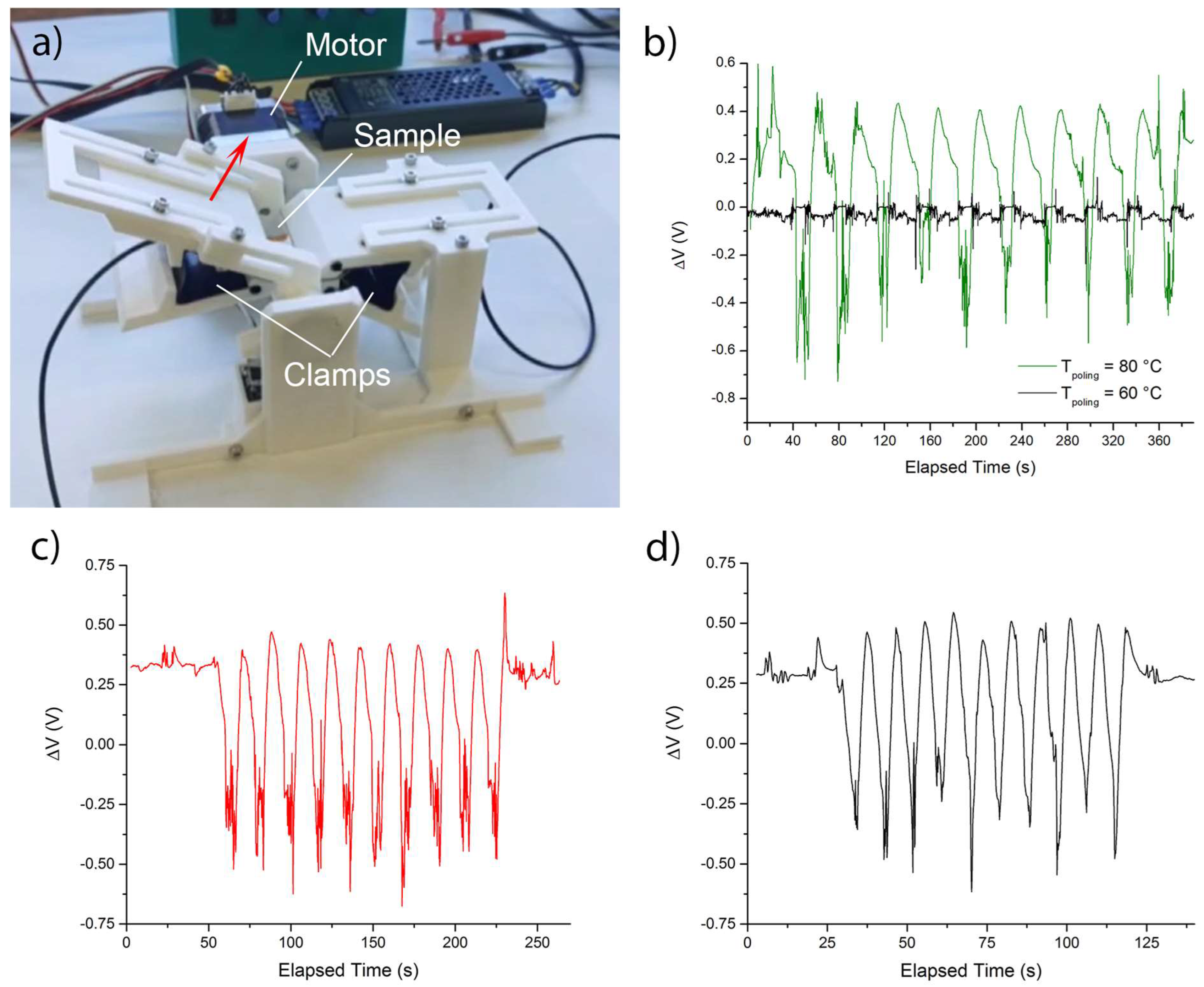
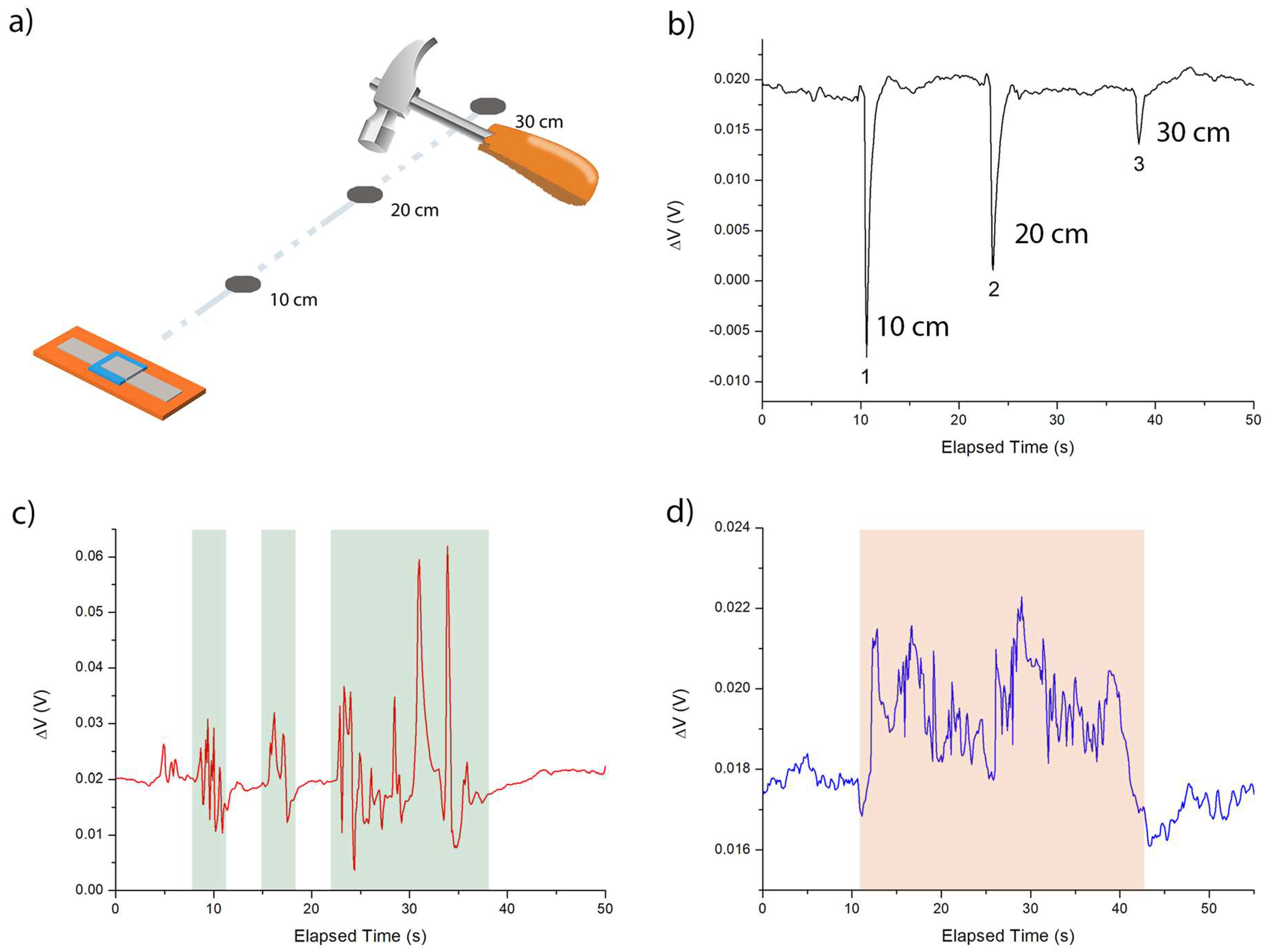
3. Results and Discussion

3.1. Sensor Printing and Characterization

The silver electrodes and the active P(VDF-TrFE) layer were inkjet-printed following the methodology elucidated in the experimental section, and the final printed sensor can be seen in Figure 1c. In order to provide some insight on the manufacturing process, its steps are characterized separately.
Initially, to evaluate the printability of the silver layers on the Kapton substrate, some preliminary studies were conducted. The morphology of the Kapton surface was studied via AFM analysis, which detected an average roughness of 16.39 nm, thus confirming the absence of relevant superficial defects. Secondly, XRD analysis was conducted, showing the presence of a semi-crystalline phase in the Kapton layer. Its occurrence was evidenced by three diffraction peaks (14.5°, 22°, and 26.1°) superimposed on an amorphous background, which can be easily seen in Figure S1. The surface was initially characterized by limited hydrophilicity, as confirmed by the contact angle (CA) measurement shown in Figure S2, which displayed a water contact angle of 53.8 ± 3.1°. Hence, to improve its wettability, the polyimide surface was treated with plasma for 3 min [44]. This surface treatment effectively enhanced the Kapton wettability, resulting in the contact angle decreasing from a value of 53.8 ± 3.1° to a value of 4.9 ± 0.8° (Figure S2). This result suggested that the surface was properly prepared for the inkjet printing of the different layers by the plasma treatment, improving the homogeneity and adhesion of the silver layer.
A silver nanoparticle ink based on organic solvents was chosen for the electrodes, since a previous work had already proven that a similar silver nanoparticle ink, also based on organic solvents, showed good adherence to plasma-treated Kapton surfaces [45]. After the printing of the bottom electrode, the XRD analysis, conducted both before (Figure S3) and after (Figure S4) the annealing process of the Ag electrode, confirmed the presence of an enhanced crystalline phase [46]. This confirmed the partial sintering of the Ag nanoparticles and the formation of a fully conductive layer. In particular, the variation in the mean dimension of the crystallites is an indicator of the partial sintering of the silver layer. The dimension of the crystallites before annealing, evaluated using Scherrer’s law on the Ag (111) peak, was equal to 27.05 nm. After annealing, the mean dimension significantly increased, to 48.77 nm. This value is in line with silver layers deposited in comparable conditions [47].
To evaluate the morphology of the resulting silver surface, a SEM analysis was conducted alongside an AFM analysis (Figure 2). Figure 2a,b show the absence of superficial defects on the bottom electrode. The AFM analysis highlighted a superficial roughness of 19.08 nm, still very close to the recorded superficial roughness of the pristine Kapton substrate (16.39 nm). This value, together with the mirror-like appearance of the layer, confirms the well-known high conformity and levelling properties typical of Ag inkjet-printed layers.
To evaluate the adherence and the mechanical resistance of the printed Ag electrode, a standardized peel test was conducted using adhesive tape. After the test, no delamination was observed. This first important result confirmed the good surface compatibility between the printed ink and the Kapton substrate and the effectiveness of the plasma treatment carried out. Moreover, to prove the electromechanical stability of the printed electrode, it was bent multiple times (20 times) at different and known bending diameters (0 cm, 2.2 cm, 1.5 cm, and 1 cm). The experiment was repeated twice under the same conditions. The electrical resistance was measured using a Fluke Voltmeter, and no mechanical delamination was observed. Average values of 1.15 ± 0.075 Ω and 1.15 ± 0.05 Ω were measured in the two repetitions, respectively, confirming the electromechanical stability of the silver layer even after a total of one hundred and twenty cycles. The resistivity of the layer was evaluated as well, considering the distance between the electrodes (10 mm), and the result was equal to 3.45 × 10⁻⁷ Ω m. This value is in line with the typical resistivity levels observed in layers composed of inkjet-printed and sintered Ag nanoparticles [48], thus confirming the good quality of the obtained layer.
A homogeneous surface, still smooth and without significant superficial defects, was observed through the SEM analysis even after the tests described above. Micro-cracks and other defects were absent, as well as mechanical delamination, thus further proving the optimal surface compatibility between the silver layer and the Kapton substrate. Furthermore, this proved experimentally that 3 min of plasma treatment on the Kapton surface is sufficient to enhance the adhesion of the chosen triethylene–glycol–monomethyl–ether-based silver nanoparticle ink up to suitable levels.
To print the active layer, the silver bottom electrode was subjected to plasma treatment for 3 min to increase its wettability. The P(VDF-TrFE) layer was then printed. The first printing tests evidenced a high level of porosity in the resulting layer (Figure S6). In fact, one of the drawbacks of this production method is that, if the inkjet printing parameters are not properly optimized, the resulting layer can be porous and full of defects. This leads to a strong capacitive effect during the poling process, and a consequent dielectric breakdown of the printed device. To overcome this inconvenience, the temperature of the nozzle plate was set at 40 °C, the printing plate was put at 60 °C, and the cartridge was changed, ensuring a proper evaporation of the solvent and a proper and more controlled ejection of the ink. This eventually led to the production of a homogeneous layer, which was confirmed by the SEM analysis conducted after the annealing process.
Finally, the Ag/active material stack was again subjected to plasma treatment for 3 min, and the top electrode was printed and annealed following the same steps employed for the bottom one. The AFM and SEM analyses (Figure 2c–f) were conducted on both layers individually. In the P(VDF-TrFE) case, it is possible to clearly distinguish the horizontal printing lines. This is due to the lower solid concentration of the PVDF-TrFE-based ink compared to silver nanoparticle-based ink and to its reduced levelling properties. Moreover, it is possible to distinguish on the surface the round defects that were caused by the evaporation of the solvents during and after the printing. The average roughness was 56.67 nm, slightly higher than the value measured on the bottom electrode, while the top one showed a remarkable final average superficial roughness of 43.24 nm. This interesting result showed that the Ag ink is characterized by good levelling properties, which typically translate into a decrease in roughness when the ink itself is printed on rough surfaces. Hence, a remarkably flat finish was maintained, confirming the optimized printing conditions, the correct and homogeneous distribution of the ink, and the probable absence of internal defects, as well. This way, the probability of incurring short-circuits or parasitic capacitive effects decreases considerably.
A SEM study was conducted on a section of the fabricated device to measure the experimental thicknesses of the printed layers. Figure 3a shows the cross-section itself, obtained by controlled breaking in liquid nitrogen. The active layer appears morphologically homogeneous, with no defects, as do the electrodes. In particular, the P(VDF-TrFE) layer contained a limited concentration of porosities, which are critical. Indeed, voids may cause short-circuits when the device is subjected to the high electric fields required for the poling step. The experimental thickness of the silver layers was seen to be 1.31 ± 0.12 µm, which is comparable to the expected value (1.5 µm, with a difference equal to 12.66%). Furthermore, the nominal thickness for the active piezoelectric layer, expected to be 3 µm after 50 layers were printed, was seen to be 2.82 ± 0.23 µm (with a 6% difference). These values of thickness were chosen because they represent an acceptable compromise between signal to noise ratio and manufacturing time. P(VDF-TrFE) layers that are too thin would indeed result in very low readout signals (due to the low polymer content of the ink) and a high probability of short-circuits. On the other hand, layers that are too thick would require an excessive number of printing cycles. In addition, active layers that are too thick have been demonstrated to yield lower signal intensity due to excessive charge separation between the two interfaces of the layer [49].
The Raman analysis performed on the active layer confirmed the predominance of the β-phase against the α-phase after the annealing process [50,51], potentially resulting in optimal piezoelectric behaviour of the device (Figure 3b). In fact, two main peaks can be distinguished in the obtained spectra, the first being around 800 cm−1 for the α-phase, and the second being around 845 cm−1 for the β-phase, as reported in the literature. The first peak can be associated with the C-C and C-F2 stretching in the α-phase, while the second is typical of C-F2 stretching in the β-phase. A third peak, associated with the C-H2 rocking in the α-phase, was detected around 880 cm−1.
The mechanical stability of the fabricated sensor was tested by bending the prototype in both concave and convex modes, as was performed for the Ag bottom electrode. Neither mechanical delamination nor wrinkling of the surface was observed. In addition, to verify the sensor’s adhesion to the Kapton substrate in extreme conditions, it was abruptly folded with a 180° fold. In this case, SEM analysis showed local micro-cracks on the surface of the top electrode, but, again, no mechanical delamination was observed on the tested specimen (Figure S5). In addition, the layers were still conductive after the bending test, maintaining an average resistance of 1.1 Ω, thus proving once more the optimal compatibility of the novel material combination here presented.

3.2. Sensor Electromechanical Testing

Finally, the overall electromechanical response of the proposed sensor was evaluated. To study the effects of poling conditions, two sensors were poled at different temperatures. Specifically, the first sensor was poled by applying a direct current (DC) voltage of 40 V for 35 min at 80 °C, whilst the second one was poled by applying a DC voltage of 40 V for 35 min at 60 °C. Despite the most common values employed in the literature for poling of bulk PVDF-TrFE starting from 20 V/μm [52], during this work it was found that 14.2 V/μm poling was sufficient for properly poling the inkjet-printed PVDF-TrFE solution. This is because during the IJP printing process, some defects, such as air bubbles, remain trapped in the printed layer, leading to a localized capacitive effect during poling. However, the reduced applied voltage did not significantly affect the performance of the active layer, as discussed below.
Both sensors were finally electromechanically tested by using a 3D-printed customized bendable structure, controlled by an Arduino motherboard (Figure 4a and Figure S7).
The experimental electromechanical results are shown in Figure 4. It was noted that, despite the lower poling voltage as compared to the bulk material and the different speeds applied to the machine and the number of cycles, the signal recorded from the sensor poled at 80 °C always maintained the same characteristics (Figure 4b–d). In detail, to compare the performance of the sensors during the different tests carried out, the mean peak-to-peak value (Vpp) of the voltage output was evaluated. This parameter was equal to 838.9 ± 51.6 mV at 100 cycles/hour, to 856.7 ± 60.6 mV at 200 cycles/hour, and to 852.6 ± 115.7 mV at 400 cycles/hour with the sensor poled at 80 °C. Considering their standard deviation, these values can be considered roughly equivalent. This suggests that the signal maintained not only the same shape, but also the same intensity. This was particularly relevant and important because it proved the repeatability of the measurements even after a relatively high number of cycles and at different bending speeds. In particular, each sensor withstood at least 100 cycles without showing appreciable variations in the shape or intensity of the output signal. The increase in standard deviation observed at increasing bending speeds can be reasonably attributed to the setup, which loses precision at high actuation speeds. The results obtained can be compared with the work carried out by Luo et al. [3], who built a sensor by PVDF direct writing and actuated it under cyclic bending conditions. The obtained response was roughly four times the one obtained in the present work (with a higher thickness of the active layer).
Regarding the effect of poling temperature, the measured value of Vpp was around 48.1 ± 4.8 mV at 100 cycles/hour for the sensor poled at 60 °C (Figure 4b). This difference with respect to the sensor poled at 80 °C, of about one order of magnitude, was attributed to the different applied poling conditions. In fact, this is the direct piezoelectric effect described by Equation (1):
D i = d i j σ j ,
where Di is the electric displacement field (C/m2), dij is the piezoelectric strain coefficient (C/N or m/V), and σj is the applied stress (N/m2 or Pa). It is known and confirmed that the piezoelectric strain coefficient highly depends on the poling temperature [53]. This confirmed that the optimal poling temperature for this customized P(VDF-TrFE)-based ink is about 80 °C. In fact, at such temperature the mobility of the polymeric chains was considerably higher than at 60 °C, thus allowing the applied voltage to rearrange the dipole orientation more efficiently while still being below the Curie temperature. In fact, in the literature it can be found that, at least for piezoceramic materials, the piezoelectric coefficient seems to be proportional to the poling temperature, according to Equation (2).
d i j 1 T p T C
where Tp is the poling temperature and Tc is the Curie temperature. This would put the optimal poling temperature at a reasonable 0.8 times Tc [54]. Despite this theoretical hypothesis referring to piezoceramics, it can probably be expanded to piezopolymeric materials as well. As the Curie temperature of our pure solid P(VDF-TrFE) is about 117 °C (value provided by the manufacturer), poling at 80 °C is definitely aligned with the theoretical values suggested by the literature.
Furthermore, in both cases the signal came back to the initial offset value when the machine was stopped, giving an approximately flat base signal after the last cycle. Finally, comparing the shapes of the signals obtained from the two different sensors (Figure 4b), it is possible to conclude that they follow a similar pattern, further demonstrating the repeatability of the measurements not only across different cycles but also across different devices. The enhancement of the output voltage observed between the two poling temperatures (60 °C and 80 °C) also constitutes clear evidence that the output signal represents the real P(VDF-TrFE) response and not a spurious output signal given by the cyclical movement of the instrumentation.
To further verify the functionality of the fabricated sensor, three additional experiments were conducted (Figure 5). In the case of the hammer thumping test (instantaneous mechanical vibration input, Figure 5a,b), the output voltage followed a decreasing trend by increasing the distance between the sensor and the hammer impact point on the table’s surface. In Figure 5c, the voltage output given by the sensor when a chair was moved on the floor close to the table (continuous mechanical vibration input) can be seen. The distance between the table and the chair was approximately 50 cm. Two distinguishable shorter stimuli and a longer one can be distinguished in the output voltage reported in Figure 5c after this experiment. All the stimuli gave a response of around 20–30 mV of amplitude. Lastly, the electromechanical response of the sensor to a vocal stimulus emitted at 5 cm from the device surface was measured, and it is reported in Figure 5d (voice input). Once again, the output voltage given by such inputs can be highlighted easily, being around 5 mV in amplitude, confirming the good sensitivity of the active layer in different sensing situations. These results were comparable to the one obtained by Luo et al. [3], even if lower in output voltage by roughly a factor of four.
In summary, all the experiments showed a consistent and defined output voltage, which came back to the starting offset once excitation was removed. This further confirmed the correct and reproducible functioning of the active layer printed with the customized P(VDF-TrFE) solution, confirming it to be a good and promising option for further studies in the flexible piezopolymer-based sensor field.

4. Conclusions

This work presented the successful design and fabrication of a fully inkjet-printed, multi-material, highly customizable, and highly flexible piezoelectric sensor. The good adhesion and mechanical properties of the chosen silver bottom electrode, inkjet-printed on a plasma-treated Kapton HN substrate, were demonstrated by a peel test, by measuring the electrical resistance obtained during its controlled bending, and by SEM analysis conducted before and after the bending test. For the first time, a P(VDF-TrFE)-based ink was inkjet-printed on top of a silver electrode on a highly flexible substrate. Subsequently, another silver electrode was inkjet-printed on top. Afterward, to evaluate the mechanical adhesion and stability of the produced sensor, controlled bending tests were performed in both concave and convex directions, and no mechanical delamination was observed. Finally, to test the electromechanical performances, identical devices were poled at two different temperatures. The effect of temperature on poling was evidenced, confirming its effect on the piezoelectric properties of the P(VDF-TrFE)-based active layer. All the fabricated sensors were bent cyclically in a controlled way from 0° to 90°, at different speeds, giving remarkably different amplitudes of output voltages according to the poling temperature employed (Vpp ≈ 850 mV for those poled at 80 °C, and Vpp ≈ 50 mV for those poled at 60 °C). However, the good and reliable piezoelectric response of the active layer was demonstrated by analysing single cycles of the measured output voltages, which were repeatable and stable along the controlled bending cycles. Afterward, the good sensitivity of the produced active layer was also demonstrated through different experiments, which indicated that the produced fully inkjet P(VDF-TrFE)-based sensor can be suitable not only for strain sensing but also for acoustic sensing. The fabricated devices were employed to sense the vibrations produced by three different external stimuli (voice, physical vibrations on the same surface, and movement of a heavy object in the same room), evidencing the full capability to detect them. Being highly customizable in shape and size, highly flexible, and potentially applicable to a wide range of surfaces, the proposed design for a piezoelectric sensor opens the opportunity to give a spatial proprioception sensation to passive structures in many applicative fields, with low-cost production and low power consumption, and avoiding the usage of harmful materials. By being applied to 4D-printed structures, for example, this sensor can be able to evaluate and give information about their shape and their position in time.

Supplementary Materials

The following supporting information can be downloaded at: https://www.mdpi.com/article/10.3390/technologies13050206/s1, Figure S1: XRD of the Kapton substrate; Figure S2: Contact angle measurement on Kapton substrate before plasma treatment (a); contact angle measurement on Kapton after three minutes of plasma treatment (b); Figure S3: XRD of the as-printed Ag electrode; Figure S4: XRD of the annealed Ag electrode; Figure S5: SEM analysis of the top electrode after being abruptly bent; Figure S6: SEM image of a highly porous P(VDF-TrFE) layer between two Ag electrodes; Figure S7: Actuation setup.

Author Contributions

G.M.: conceptualization, data curation, formal analysis, investigation, methodology, validation, visualization, writing—original draft, writing—review and editing. R.B.: conceptualization, methodology, investigation, visualization, supervision, writing—original draft, writing—review and editing. V.Z.: conceptualization, validation, visualization, supervision, writing—original draft, writing—review and editing. R.S.: validation, writing—review and editing. M.M.: investigation, visualization. G.B.: validation, supervision, resources. A.C.: validation, resources. L.M.: methodology, project administration, resources. All authors have read and agreed to the published version of the manuscript.

Funding

This work was partially supported by the ERC advanced grant IMMENSE—101140720.

Data Availability Statement

The original contributions presented in this study are included in the article/Supplementary Materials. Further inquiries can be directed to the corresponding author.

Acknowledgments

This work was carried out in the framework of the interdepartmental laboratory MEMS&3D of Politecnico di Milano, Italy.

Conflicts of Interest

The authors declare that they have no known competing financial interests or personal relationships that could have influenced the work described in the present paper.

References

  1. Javaid, M.; Haleem, A.; Singh, R.P.; Rab, S.; Suman, R. Significance of Sensors for Industry 4.0: Roles, Capabilities, and Applications. Sens. Int. 2021, 2, 100110. [Google Scholar] [CrossRef]
  2. Dagdeviren, C.; Joe, P.; Tuzman, O.L.; Park, K.I.; Lee, K.J.; Shi, Y.; Huang, Y.; Rogers, J.A. Recent Progress in Flexible and Stretchable Piezoelectric Devices for Mechanical Energy Harvesting, Sensing and Actuation. Extrem. Mech. Lett. 2016, 9, 269–281. [Google Scholar] [CrossRef]
  3. Luo, J.; Zhang, L.; Wu, T.; Song, H.; Tang, C. Flexible Piezoelectric Pressure Sensor with High Sensitivity for Electronic Skin Using Near-Field Electrohydrodynamic Direct-Writing Method. Extrem. Mech. Lett. 2021, 48, 101279. [Google Scholar] [CrossRef]
  4. Sun, R.; Carreira, S.C.; Chen, Y.; Xiang, C.; Xu, L.; Zhang, B.; Chen, M.; Farrow, I.; Scarpa, F.; Rossiter, J. Stretchable Piezoelectric Sensing Systems for Self-powered and Wireless Health Monitoring. Adv. Mater. Technol. 2019, 4, 1900100. [Google Scholar] [CrossRef]
  5. Matsuhisa, N.; Kaltenbrunner, M.; Yokota, T.; Jinno, H.; Kuribara, K.; Sekitani, T.; Someya, T. Printable Elastic Conductors with a High Conductivity for Electronic Textile Applications. Nat. Commun. 2015, 6, 7461. [Google Scholar] [CrossRef]
  6. Zhao, Z.; Tang, J.; Yuan, J.; Li, Y.; Dai, Y.; Yao, J.; Zhang, Q.; Ding, S.; Li, T.; Zhang, R. Large-Scale Integrated Flexible Tactile Sensor Array for Sensitive Smart Robotic Touch. ACS Nano 2022, 16, 16784–16795. [Google Scholar] [CrossRef]
  7. Moonen, P.F.; Yakimets, I.; Huskens, J. Fabrication of Transistors on Flexible Substrates: From Mass-printing to High-resolution Alternative Lithography Strategies. Adv. Mater. 2012, 24, 5526–5541. [Google Scholar] [CrossRef]
  8. Lü, X.; Jiang, J.; Wang, H.; Gao, Q.; Zhao, S.; Li, N.; Yang, J.; Wang, S.; Bao, W.; Chen, R. Sensitivity-Compensated Micro-Pressure Flexible Sensor for Aerospace Vehicle. Sensors 2018, 19, 72. [Google Scholar] [CrossRef]
  9. Tung, S.; Witherspoon, S.R.; Roe, L.A.; Silano, A.; Maynard, D.P.; Ferraro, N. A MEMS-Based Flexible Sensor and Actuator System for Space Inflatable Structures. Smart Mater. Struct. 2001, 10, 1230. [Google Scholar] [CrossRef]
  10. Li, Z.; Liu, Y.; Hossain, O.; Paul, R.; Yao, S.; Wu, S.; Ristaino, J.B.; Zhu, Y.; Wei, Q. Real-Time Monitoring of Plant Stresses via Chemiresistive Profiling of Leaf Volatiles by a Wearable Sensor. Matter 2021, 4, 2553–2570. [Google Scholar] [CrossRef]
  11. Naqi, M.; Lee, S.; Kwon, H.; Lee, M.G.; Kim, M.; Kim, T.W.; Shin, H.K.; Kang, S.; Gandla, S.; Lee, H. A Fully Integrated Flexible Heterogeneous Temperature and Humidity Sensor-based Occupancy Detection Device for Smart Office Applications. Adv. Mater. Technol. 2019, 4, 1900619. [Google Scholar] [CrossRef]
  12. Xie, Z.; Avila, R.; Huang, Y.; Rogers, J.A. Flexible and Stretchable Antennas for Biointegrated Electronics. Adv. Mater. 2020, 32, 1902767. [Google Scholar] [CrossRef]
  13. Zhong, D.; Wu, C.; Jiang, Y.; Yuan, Y.; Kim, M.; Nishio, Y.; Shih, C.-C.; Wang, W.; Lai, J.-C.; Ji, X. High-Speed and Large-Scale Intrinsically Stretchable Integrated Circuits. Nature 2024, 627, 313–320. [Google Scholar] [CrossRef] [PubMed]
  14. Huang, T.-C.; Fukuda, K.; Lo, C.-M.; Yeh, Y.-H.; Sekitani, T.; Someya, T.; Cheng, K.-T. Pseudo-CMOS: A Design Style for Low-Cost and Robust Flexible Electronics. IEEE Trans. Electron Devices 2010, 58, 141–150. [Google Scholar] [CrossRef]
  15. Zhu, C.; Chortos, A.; Wang, Y.; Pfattner, R.; Lei, T.; Hinckley, A.C.; Pochorovski, I.; Yan, X.; To, J.W.-F.; Oh, J.Y. Stretchable Temperature-Sensing Circuits with Strain Suppression Based on Carbon Nanotube Transistors. Nat. Electron. 2018, 1, 183–190. [Google Scholar] [CrossRef]
  16. Lee, T.; Lee, W.; Kim, S.; Kim, J.J.; Kim, B. Flexible Textile Strain Wireless Sensor Functionalized with Hybrid Carbon Nanomaterials Supported ZnO Nanowires with Controlled Aspect Ratio. Adv. Funct. Mater. 2016, 26, 6206–6214. [Google Scholar] [CrossRef]
  17. Kong, H.; Song, Z.; Li, W.; Chen, M.; Bao, Y.; Liu, Z.; Qu, D.; Ma, Y.; Wang, Z.; Han, D. A Self-Protective Piezoelectric-Piezoresistive Dual-Mode Device with Superior Dynamic-Static Mechanoresponse and Energy Harvesting Performance Enabled by Flextensional Transduction. Nano Energy 2022, 100, 107498. [Google Scholar] [CrossRef]
  18. Vetelino, J.; Reghu, A. Introduction to Sensors; CRC Press: Boca Raton, FL, USA, 2017; ISBN 1315218275. [Google Scholar]
  19. Yiu, C.; Wong, T.H.; Liu, Y.; Yao, K.; Zhao, L.; Li, D.; Hai, Z.; Zheng, H.; Wang, Z.; Yu, X. Skin-like Strain Sensors Enabled by Elastomer Composites for Human–Machine Interfaces. Coatings 2020, 10, 711. [Google Scholar] [CrossRef]
  20. Nishikawa, T.; Yamane, H.; Matsuhisa, N.; Miki, N. Stretchable Strain Sensor with Small but Sufficient Adhesion to Skin. Sensors 2023, 23, 1774. [Google Scholar] [CrossRef]
  21. Glinsek, S.; Song, L.; Kovacova, V.; Mahjoub, M.A.; Godard, N.; Girod, S.; Biagi, J.; Quintana, R.; Schleeh, T.; Guedra, M. Inkjet-printed Piezoelectric Thin Films for Transparent Haptics. Adv. Mater. Technol. 2022, 7, 2200147. [Google Scholar] [CrossRef]
  22. Bernasconi, R.; Hatami, D.; Hosseinabadi, H.N.; Zega, V.; Corigliano, A.; Suriano, R.; Levi, M.; Langfelder, G.; Magagnin, L. Hybrid Additive Manufacturing of a Piezopolymer-Based Inertial Sensor. Addit. Manuf. 2022, 59, 103091. [Google Scholar] [CrossRef]
  23. Luo, Y.; Abidian, M.R.; Ahn, J.-H.; Akinwande, D.; Andrews, A.M.; Antonietti, M.; Bao, Z.; Berggren, M.; Berkey, C.A.; Bettinger, C.J. Technology Roadmap for Flexible Sensors. ACS Nano 2023, 17, 5211–5295. [Google Scholar] [CrossRef] [PubMed]
  24. Maeder, M.D.; Damjanovic, D.; Setter, N. Lead Free Piezoelectric Materials. J. Electroceram. 2004, 13, 385–392. [Google Scholar] [CrossRef]
  25. Narita, F.; Fox, M. A Review on Piezoelectric, Magnetostrictive, and Magnetoelectric Materials and Device Technologies for Energy Harvesting Applications. Adv. Eng. Mater. 2018, 20, 1700743. [Google Scholar] [CrossRef]
  26. Mensur Alkoy, E.; Dagdeviren, C.; Papila, M. Processing Conditions and Aging Effect on the Morphology of PZT Electrospun Nanofibers, and Dielectric Properties of the Resulting 3–3 PZT/Polymer Composite. J. Am. Ceram. Soc. 2009, 92, 2566–2570. [Google Scholar] [CrossRef]
  27. Nguyen, T.D.; Deshmukh, N.; Nagarah, J.M.; Kramer, T.; Purohit, P.K.; Berry, M.J.; McAlpine, M.C. Piezoelectric Nanoribbons for Monitoring Cellular Deformations. Nat. Nanotechnol. 2012, 7, 587–593. [Google Scholar] [CrossRef]
  28. Dagdeviren, C.; Shi, Y.; Joe, P.; Ghaffari, R.; Balooch, G.; Usgaonkar, K.; Gur, O.; Tran, P.L.; Crosby, J.R.; Meyer, M. Conformal Piezoelectric Systems for Clinical and Experimental Characterization of Soft Tissue Biomechanics. Nat. Mater. 2015, 14, 728–736. [Google Scholar] [CrossRef]
  29. Hong, C.-C.; Huang, S.-Y.; Shieh, J.; Chen, S.-H. Enhanced Piezoelectricity of Nanoimprinted Sub-20 Nm Poly (Vinylidene Fluoride–Trifluoroethylene) Copolymer Nanograss. Macromolecules 2012, 45, 1580–1586. [Google Scholar] [CrossRef]
  30. Kawai, H. The Piezoelectricity of Poly (Vinylidene Fluoride). Jpn. J. Appl. Phys. 1969, 8, 975. [Google Scholar] [CrossRef]
  31. Durand, N.; Ameduri, B.; Takashima, K.; Ishida, K.; Horie, S.; Ueda, Y. Vinylidene Fluoride Telomers for Piezoelectric Devices. Polym. J. 2011, 43, 171–179. [Google Scholar] [CrossRef]
  32. Tait, J.G.; Witkowska, E.; Hirade, M.; Ke, T.-H.; Malinowski, P.E.; Steudel, S.; Adachi, C.; Heremans, P. Uniform Aerosol Jet Printed Polymer Lines with 30 Μm Width for 140 Ppi Resolution RGB Organic Light Emitting Diodes. Org. Electron. 2015, 22, 40–43. [Google Scholar] [CrossRef]
  33. Mandal, A.; Morali, A.; Skorobogatiy, M.; Bodkhe, S. 3D Printing of Polyvinylidene Fluoride-Based Piezoelectric Sensors for Noninvasive Continuous Blood Pressure Monitoring. Adv. Eng. Mater. 2024, 26, 2301292. [Google Scholar] [CrossRef]
  34. Nassar, H.; Khandelwal, G.; Chirila, R.; Karagiorgis, X.; Ginesi, R.E.; Dahiya, A.S.; Dahiya, R. Fully 3D Printed Piezoelectric Pressure Sensor for Dynamic Tactile Sensing. Addit. Manuf. 2023, 71, 103601. [Google Scholar] [CrossRef]
  35. Schaumann, S.; Latsch, B.; Schäfer, N.; Dali, O.B.; Seiler, J.; Raynaud, J.; Grimmer, M.; Flor, H.; Beckerle, P.; Kupnik, M. Force Myography for Motion Intention Detection Based on 3D-Printed Piezoelectric Sensors. IEEE Sensors Lett. 2024, 8. [Google Scholar] [CrossRef]
  36. Jiang, C.; Choi, H.W.; Cheng, X.; Ma, H.; Hasko, D.; Nathan, A. Printed Subthreshold Organic Transistors Operating at High Gain and Ultralow Power. Science 2019, 363, 719–723. [Google Scholar] [CrossRef] [PubMed]
  37. Afanasenkau, D.; Kalinina, D.; Lyakhovetskii, V.; Tondera, C.; Gorsky, O.; Moosavi, S.; Pavlova, N.; Merkulyeva, N.; Kalueff, A.V.; Minev, I.R. Rapid Prototyping of Soft Bioelectronic Implants for Use as Neuromuscular Interfaces. Nat. Biomed. Eng. 2020, 4, 1010–1022. [Google Scholar] [CrossRef]
  38. Kipphan, H. Handbook of Print Media: Technologies and Production Methods; Springer Science & Business Media: Berlin/Heidelberg, Germany, 2001; ISBN 3540673261. [Google Scholar]
  39. Haque, R.I.; Vié, R.; Germainy, M.; Valbin, L.; Benaben, P.; Boddaert, X. Inkjet Printing of High Molecular Weight PVDF-TrFE for Flexible Electronics. Flex. Print. Electron. 2015, 1, 15001. [Google Scholar] [CrossRef]
  40. Bhavanasi, V.; Kumar, V.; Parida, K.; Wang, J.; Lee, P.S. Enhanced Piezoelectric Energy Harvesting Performance of Flexible PVDF-TrFE Bilayer Films with Graphene Oxide. ACS Appl. Mater. Interfaces 2016, 8, 521–529. [Google Scholar] [CrossRef]
  41. Trung, T.Q.; Lee, N. Flexible and Stretchable Physical Sensor Integrated Platforms for Wearable Human-activity Monitoringand Personal Healthcare. Adv. Mater. 2016, 28, 4338–4372. [Google Scholar] [CrossRef]
  42. Shehata, N.; Nair, R.; Boualayan, R.; Kandas, I.; Masrani, A.; Elnabawy, E.; Omran, N.; Gamal, M.; Hassanin, A.H. Stretchable Nanofibers of Polyvinylidenefluoride (PVDF)/Thermoplastic Polyurethane (TPU) Nanocomposite to Support Piezoelectric Response via Mechanical Elasticity. Sci. Rep. 2022, 12, 8335. [Google Scholar]
  43. Xie, M.; Zhu, M.; Yang, Z.; Okada, S.; Kawamura, S. Flexible Self-Powered Multifunctional Sensor for Stiffness-Tunable Soft Robotic Gripper by Multimaterial 3D Printing. Nano Energy 2021, 79, 105438. [Google Scholar] [CrossRef]
  44. Inagaki, N.; Tasaka, S.; Hibi, K. Surface Modification of Kapton Film by Plasma Treatments. J. Polym. Sci. Part A Polym. Chem. 1992, 30, 1425–1431. [Google Scholar] [CrossRef]
  45. Fang, Y.; Tentzeris, M.M. Surface Modification of Polyimide Films for Inkjet-Printing of Flexible Electronic Devices. In Flexible Electronics; IntechOpen: London, UK, 2018; ISBN 1789234573. [Google Scholar]
  46. Zhang, D.Y.; Liu, J.; Shi, Y.S.; Wang, Y.; Liu, H.F.; Hu, Q.L.; Su, L.; Zhu, J. Antifouling Polyimide Membrane with Surface-Bound Silver Particles. J. Memb. Sci. 2016, 516, 83–93. [Google Scholar] [CrossRef]
  47. Haque, R.I.; Ogam, E.; Loussert, C.; Benaben, P.; Boddaert, X. Fabrication of Capacitive Acoustic Resonators Combining 3D Printing and 2D Inkjet Printing Techniques. Sensors 2015, 15, 26018–26038. [Google Scholar] [CrossRef]
  48. Perelaer, J.; Smith, P.J.; Mager, D.; Soltman, D.; Volkman, S.K.; Subramanian, V.; Korvink, J.G.; Schubert, U.S. Printed Electronics: The Challenges Involved in Printing Devices, Interconnects, and Contacts Based on Inorganic Materials. J. Mater. Chem. 2010, 20, 8446–8453. [Google Scholar] [CrossRef]
  49. Zhang, J.; Zhu, P.; Ouyang, H.; Wang, E.; Xue, J.; Li, Z.; Shi, B.; Fan, Y. High Signal to Noise Ratio Piezoelectric Thin Film Sensor Based on Elastomer Amplification for Ambulatory Blood Pressure Monitoring. ACS Sens. 2024, 9, 1301–1309. [Google Scholar] [CrossRef] [PubMed]
  50. Jia, N.; He, Q.; Sun, J.; Xia, G.; Song, R. Crystallization Behavior and Electroactive Properties of PVDF, P(VDF-TrFE) and Their Blend Films. Polym. Test. 2017, 57, 302–306. [Google Scholar] [CrossRef]
  51. Arrigoni, A.; Brambilla, L.; Bertarelli, C.; Serra, G.; Tommasini, M.; Castiglioni, C.P. (VDF-TrFE) Nanofibers: Structure of the Ferroelectric and Paraelectric Phases through IR and Raman Spectroscopies. RSC Adv. 2020, 10, 37779–37796. [Google Scholar] [CrossRef]
  52. McGinn, C.K.; Kam, K.A.; Laurila, M.-M.; Lozano Montero, K.; Mäntysalo, M.; Lupo, D.; Kymissis, I. Formulation, Printing, and Poling Method for Piezoelectric Films Based on PVDF–TrFE. J. Appl. Phys. 2020, 128, 225304. [Google Scholar] [CrossRef]
  53. Martins, P.; Lopes, A.C.; Lanceros-Mendez, S. Electroactive Phases of Poly (Vinylidene Fluoride): Determination, Processing and Applications. Prog. Polym. Sci. 2014, 39, 683–706. [Google Scholar] [CrossRef]
  54. Haertling, G.H. Ferroelectric Ceramics: History and Technology. J. Am. Ceram. Soc. 1999, 82, 797–818. [Google Scholar] [CrossRef]
Figure 1. Scheme of the printing process of the proposed sensor (a): substrate preparation (I), silver bottom electrode inkjet printing (II), P(VDF-TrFE) active layer inkjet printing (III), silver top electrode inkjet printing (IV); schematic view of the sensor cross-section (b), where nominal thickness is reported for each layer; photo of the fabricated sensor (c).
Technologies 13 00206 g001
Figure 2. AFM analysis (a,c,e) and SEM analysis (b,d,f) of the bottom silver electrode (a,b), PVDF-TrFE (c,d), and the top silver electrode (e,f).
Technologies 13 00206 g002
Figure 3. SEM image of the fabricated device’s cross-section (a); Raman spectrum of the DMSO/MEK 70/30%wt. and PVDF-TrFE 0.7%wt. printed and annealed solution (b).
Technologies 13 00206 g003
Figure 4. Bending setup employed during the tests (a); comparison between the output voltages measured by the two sensors poled at different temperatures when a deformation speed of 100 cycles/hour is applied (b); output voltage of the sensor poled at 80 °C when a deformation speed of 200 cycles/hour is applied (c); output voltage of the sensor poled at 80 °C when a deformation speed of 400 cycles/hour is applied (d).
Technologies 13 00206 g004
Figure 5. Schematic representation of the experimental setup (a); output voltage measured during thumping with a hammer on the table surface at different horizontal distances from the sample (10 cm, 20 cm, and 30 cm in distance) (b); output voltage measured while a chair on the floor was being moved (c); output voltage measured while sensing a human voice (d).
Technologies 13 00206 g005
Disclaimer/Publisher’s Note: The statements, opinions and data contained in all publications are solely those of the individual author(s) and contributor(s) and not of MDPI and/or the editor(s). MDPI and/or the editor(s) disclaim responsibility for any injury to people or property resulting from any ideas, methods, instructions or products referred to in the content.

