Article

Open-Source Hardware Design of Modular Solar DC Nanogrid

by
Md Motakabbir Rahman
1,2,
Sara Khan
2 and
Joshua M. Pearce
1,2,3,*
1
Department of Electrical & Computer Engineering, Western University, London, ON N6A 5B9, Canada
2
FAST Lab, Western University, London, ON N6A 5B9, Canada
3
Ivey School of Business, Western University, London, ON N6G 0N1, Canada
*
Author to whom correspondence should be addressed.
Technologies 2024, 12(9), 167; https://doi.org/10.3390/technologies12090167
Submission received: 31 July 2024 / Revised: 30 August 2024 / Accepted: 11 September 2024 / Published: 13 September 2024
(This article belongs to the Section Environmental Technology)

Abstract

:
The technical feasibility of solar photovoltaic (PV) direct current (DC) nanogrids is well established, but the components of nanogrids are primarily commercially focused on alternating current (AC)-based systems. Thus, DC converter-based designs at the system level require personnel with high degree of technical knowledge, which results in high costs. To enable a democratization of the technology by reducing the costs, this study provides a novel modular plug-and-play open-source DC nanogrid. The system can be customized according to consumer requirements, enabling the supply of various voltage levels to accommodate different device voltage needs. The step-by-step design process of the converter, controller, data logger, and assembly of the complete system is provided. A time-domain simulation and stability analysis of the designed system were conducted in MATLAB/Simulink (version 2024b) as well as experimental validation. The results show that transforming the nanogrid from a distribution network to a device makes it suitable for various user-specific applications, such as remotely supplying power to campsites, emergency vehicles like ambulances, and small houses lacking grid electricity. The modular DC nanogrid includes all the features available in a DC distribution network, as well as data logging, which enhances the user experience and promotes the use of solar-powered DC grid systems.

1. Introduction

The nanogrid functions as a fundamental unit in a distribution network combining renewable and conventional power resources. Typically, it is referred to as a building block of microgrids, which are systems that integrate multiple conventional power sources and distributed energy resources to supply power to a large area [1]. A microgrid can typically be divided into a network of nanogrids, each serving localized power demands within the smaller area coverage [2]. The difference between microgrids and nanogrid is based on their power supply capability and the range over which they can distribute power. A nanogrid is defined as a standalone DC distribution network that integrates distributed renewable energy resources to supply electricity to a small cluster of loads [3]. To be classified as a nanogrid, the system must meet a power requirement in the range of few watts to 5 kW for residential loads [4]. Based on its power-supplying capability, a nanogrid is suitable for small specific systems that may be completely isolated from the grid network or may be connected to the grid for uninterruptible power supply.
Solar photovoltaic (PV) systems stand out for their sustainability [5], low-cost [6] effectiveness, and reliability [7] among renewable energy options [8]. Solar energy is a promising resource in most tropical regions and areas with extended daylight hours across the globe [9,10]. In addition, recent PV cost decline [11] has made it the lowest-cost source of power in most of the world [12]. Thus, solar DC nanogrid is gaining attention worldwide for meeting electrical demands and is suggested for places where grid electricity remains inaccessible [13]. A solar DC nanogrid can save up to 25% of the cost for a specific area in Kutubdia, Bangladesh, by eliminating the use of inverters [14]. An analysis of the economics of a solar DC nanogrid in a region of KwaZulu-Natal Province, South Africa [15], and in Nigeria [16] showed that the net cost of energy was significantly lower than that of a diesel generator. In addition, the future of null net energy buildings can be achieved by practically implementing DC nanogrids [17]. Small-scale nanogrids are being implemented worldwide, particularly in regions with expensive grid electricity or inadequate grid coverage [18]. The availability of various tabletop appliances that directly operate on DC made the implementation of DC nanogrids easier and more logical [19]. Those appliances include LED lights, laptops, mobile chargers, televisions, computers, and even DC-based appliances like refrigerators. Taking advantage of appliances operating directly on DC, the implementation of DC-based homes have been completed in many locations, including the US, Indonesia, and Philippines to supply basic household loads at a voltage level of 48 V DC [20,21]. In a small DC network, smart sockets along with a communication network were integrated to control and measure all the devices that are connected to the system. From the DC nanogrid setup, substantial power savings (around 30%) were obtained compared with AC [22]. There have been numerous implementations of DC nanogrid systems. For instance, a hybrid nanogrid integrating solar PV, wind turbines, and batteries as distributed energy resources was successfully installed to supply local loads [23]. In addition, a DC nanogrid system that was capable of generating and distributing power up to 1.2 kW in a voltage level of 24 V was also designed [24]. Furthermore, two DC voltage levels, 380 V and 48 V, were proposed and experimentally validated for compatibility with conventional AC-powered appliances [25].
So, the feasibility of a solar DC nanogrid has already been established, with most of the nanogrid components being well-defined. The converter technologies, maximum power point tracker (MPPT), and battery charge controller technologies are well-established products that are used in conventional solar PV nanogrid systems. But these systems are designed for use in AC systems, and as a result, DC converter-based designs at the system level require personnel with high technical knowledge for proper design, connection, and integration of all components [26]. They are not readily available in the market for nanogrid use. The hardware implementation of the DC nanogrid is challenging for the average user because it requires extensive technical expertise to ensure the safe and proper operation of all components, including converters, controllers, energy storage systems, and monitoring devices [27]. This raises costs and limits the wide acceptance of the proven technology.
To address this issue, this article provides a novel innovation: a modular version of the DC nanogrid to be installed at consumer premises in a device form, operating as a plug-and-play device that can be customized according to consumer requirements. The design follows open hardware best practices to ensure maximum accessibility [28,29]. Earlier, the architecture, controller design, stability analysis, and a novel energy management system (EMS) of modular DC nanogrid were proposed [30]; here, this paper introduces the first hardware setup of a modular, plug-and-play open-source nanogrid device, operable with minimal technical expertise, akin to other consumer electronics available on the market. This modular DC nanogrid can be easily customized according to consumers’ power requirements, enabling the supply of various voltage levels to accommodate different device voltage needs. All designs utilize open-source hardware and software, ensuring accessibility for users worldwide. The step-by-step design process of the converter, controller, data logger, and assembly of the complete system is provided. A time-domain simulation and stability analysis of the designed system were conducted in MATLAB/Simulink. Subsequently, the connection and disconnection of a 30 W load were observed to assess the stability of the designed hardware. The results are presented and discussed in the context of transforming the nanogrid from a distribution network or system to a device, which makes it suitable for various user-specific applications, such as remotely supplying power to camp vehicles, campsites, emergency vehicles like ambulances, and small houses lacking grid electricity.

2. Materials and Methods

2.1. System Architecture

The novel nanogrid architecture the authors developed for this article is shown in Figure 1. The PV converter connects the PV modules to the DC grid, while bidirectional battery converters and load converters link lithium-ion (Li-ion) batteries and various loads to the grid. Among the low voltage levels (12 V to 100 V), 48 V is identified as the optimal choice based on cost and performance. The nanogrid design is scalable; additional PV modules and interface converters can be added to the bus to increase generation capacity. Similarly, extra batteries can be integrated using additional battery converters to support increased loads or storage needs. The EMS can manage variations in DC load and weather conditions, enhancing the system’s modularity and adaptability.
In the nanogrid, the battery discharges only in power deficit mode, defined by a bus voltage below 48 V. The controller compares the bus voltage with a reference value, initiating battery discharge to raise the bus voltage to 48 V. In power surplus mode when bus voltage is above 48 V, the controller lowers the bus voltage to reference 48 V and initiates battery charging. Three different levels of load can be served using a step-down load converter, and loads rated at 48 V can be directly connected to the bus, as the bus voltage remains stable.

2.2. Converter Topology for DC Nanogrid

A nanogrid has the potential to function independently without integrating with the AC grid, but the intermittent nature of renewable energy resources may necessitate connecting the AC grid to the DC distribution network to ensure a continuous power supply. This connection requires an AC/DC converter to link the AC supply to the bus network. The smooth operation of the DC nanogrid largely depends on the stability of the bus voltage. Given the possibility of multiple distributed energy resources being connected to the DC nanogrid, along with battery storage or an external utility grid (or both) for continuous power supply, controlling the bus voltage becomes crucial. This is where electronic power converters come into play. Power converters act as interfaces for each element connected to the DC bus, each with a different role, but ultimately ensuring the stability of the entire nanogrid system. As such, extensive studies are conducted to identify the best architecture for these converters. Various topologies examined in terms of design, modes of operation, and control mechanisms to optimize the performance and stability of the nanogrid are summarized in Table 1.
For connecting the battery to the DC bus, various bidirectional converters are employed, including high-gain bidirectional converters and fourth-order bidirectional converters (FoBiDC), which minimize ripples and enhance grid stability. To mitigate the intermittent nature of PV, two-stage PWM bidirectional converters, two-stage bidirectional grid interface converters (BGIC), and cascaded bidirectional converters are utilized. These configurations typically incorporate a DC-DC converter followed by a rectifier circuit, facilitating grid integration with the nanogrid and improving system stability. While researchers are exploring more efficient converter topologies, the absence of a modular multi-converter-based nanogrid system that supports easy integration and expansion remains a gap. This research is motivated to prioritize the hardware development of nanogrid systems, setting aside advanced converter topologies and AC grid integration for future exploration, despite their potential benefits.

2.3. Design of Controllers

The nanogrid controller coordinates various power sources to achieve optimal power flow. The energy management system (EMS) proposed in [30] maintains this coordination and dispatches the required power levels demanded by the load. Various control strategies can be implemented, which are broadly classified into centralized, decentralized, and hybrid control topologies [39].
In the centralized control method, a central controller manages the power, voltage, and load of the nanogrid using data from various sources and loads, communicated through a network, with all units in the nanogrid directly interfacing with the central controller. This central controller makes decisions based on information collected from sensors attached to all sources and loads via communication channels. While this strategy is fast and precise, it has a significant drawback: a single communication link failure can lead to the total grid failure [40]. In contrast, the decentralized control scheme has each unit in the nanogrid collect local information from sources or loads through individual sensors. This approach is more robust and reliable as it avoids costly communication links [41]. Coordination between units, fault management, and overall system data monitoring, however, become more challenging [42]. Hybrid distributed control combines elements of both distributed and decentralized control. In the hybrid topology, converters in the nanogrid communicate with each other to create a cohesive control strategy and share information with the central master controller. Local control decisions are made by local controllers, while the central master controller oversees the entire system and makes broader decisions. This approach enhances system reliability by eliminating dependence on a dedicated communication link all the time and makes the system more resistant to failures.
In this modular open-source DC nanogrid system, a hybrid control technique is used to implement the EMS. Converters manage source and load-level control, while a dedicated central controller coordinates each unit, as shown in Figure 2. Communication between the units and the central controller occurs through two methods. Critical information is shared via the digital pins of the Arduino microcontroller, with specific pins dedicated to the PV controller and the battery converter to indicate their modes, and the other is for the master controller to manage all units. Additionally, the master controller connects to all converters using an I2C (Inter Integrated Circuit) path, which is a two-wire serial communication protocol using a serial data line and a serial clock line. This allows the central controller to collect local information cyclically and to interrupt, control, or send commands to each converter as needed [43]. This hybrid approach delivers a powerful and fast control system with enhanced resilience to failure.

2.3.1. PV Controller Design

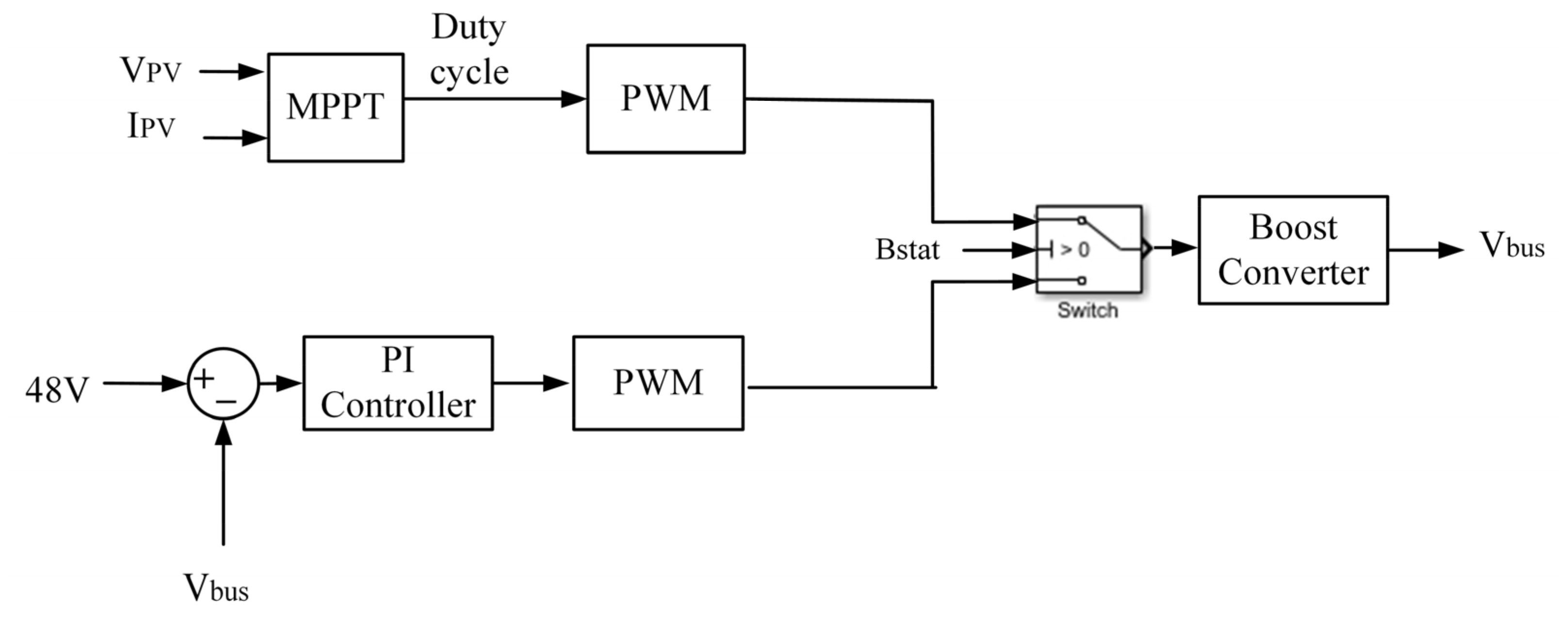
Based on the battery charging status and state of charge (SOC), the PV controller operates in two different modes. When the battery is in a constant current charging state and connected to the system, the PV controller operates in MPPT mode. In this mode, the controller maximizes the input power from the PV using an MPPT algorithm implemented through PWM control, while the battery regulates the bus voltage. When the battery is nearly charged and in a constant voltage charging state where the charging current depends only on the battery SOC or when the battery is fully discharged and the PV is connected to the system, the PV switches to bus control mode. In this mode, the converter maintains the bus voltage at a defined 48 V using a PI controller. The schematic diagram of this PV controller is given in Figure 3.
Generally, the cost of commercial MPPT devices is significantly higher than that of solar charge controllers, making them less accessible and affordable for users [44]. Previous work has shown that a successful strategy for accelerating innovation and lowering hardware costs is to use an open-source design [45,46]. Previous studies have argued open source design should be applied to PV systems and components to reduce costs [47]. Following that theory, to help make small solar PV systems more economically accessible and easier inclusion in the DC bus an efficient MPPT PV converter is designed, in this study a new open-source MPPT is designed to reduce the price gap between MPPT and solar charge controllers. There has been some open-source hardware development in the electronics of PV systems [48,49], which began with the design of smart monitoring systems for different PV applications; majority of these systems used Arduino microcontrollers for conditioning and processing the output signals of the sensors and were flexible, modular, scalable, and of low cost [50]. A prototype of an MPPT using the microcontroller PIC16F877A was designed for 10 W power, which is very low power and not suitable for most applications or commercial use [51].
Different tracking methods were introduced in the MPPT hardware, such as particle swarm optimization (PSO) technique [52] and incremental conductance algorithm [53]. These MPPT methods can be categorized into four groups: conventional, intelligent, optimization, and hybrid techniques [54]. Among the conventional MPPT methods, the variable step size incremental conductance MPPT algorithm automatically adjusts the step size to improve MPPT speed and accuracy. The step size is determined based on the derivative of power to voltage of the PV array [55]. Conventional methods are less effective under partial shading and have slower response times, whereas intelligent, optimization and hybrid techniques can handle partial shading [56,57]. Optimization methods like PSO [58], firefly algorithm (FA), and ant colony optimization (ACO) are the best for extracting power from PV under partial shading conditions as they are more accurate but require expensive hardware [59,60]. Among all these methods, the perturb and observe (P&O) method is the most popular and widely used, while artificial intelligence-based methods are fast and stable but require digital applications and multiple sensors [61]. Thus, in this design, a modified P&O method is used due to less complexity and comparatively faster tracking capability. Many modified versions of P&O have been developed, which use converter duty cycle as the perturbed signal or adaptive perturbation values [62]. The fundamental concept of the P&O algorithm is to adjust the perturbation amplitude according to the present operational conditions. In the case of the PV controller in DC nanogrid, it takes the PV voltage and current as an input and generates the optimal duty cycle for the converter.

2.3.2. Battery Controller Design for Bidirectional Converter

The battery controller determines the charging and discharging modes based on the bus voltage and the SOC of the battery. Any surplus energy in the grid increases the bus voltage, indicating a charging state, and vice versa. The SOC or battery voltage indicates the charging state. Depending on this, the battery can be charged in constant current mode or constant voltage mode, as shown in Figure 4.
In the constant current mode, the battery is charged at a fixed current, which is below its maximum charging current rating. This mode is typically employed when the battery’s charge is below approximately 90% to 95% of its full capacity [63]. Constant current charging is challenging with solar power, however, due to the variable nature of energy from solar cells. During this phase, the bidirectional converter leverages available PV power to charge the battery, with the charging current constrained to the battery’s rated capacity [64]. Once the battery approaches full charge, it no longer accepts high currents, which could otherwise lead to excess energy in the bus and increase the voltage. To address this, the system is designed with a maximum charging voltage threshold. When the battery reaches this voltage, the charging strategy shifts from constant current to the constant voltage mode. In this mode, the battery only accepts current within its allowable limits, which is set by the BMS inside the battery, and the PV system operates in the constant bus voltage mode. This adjustment ensures that the PV system provides only the power required by the system at that moment, preventing overcharging and managing the energy flow effectively [65]. This charging strategy is well suited for modern lithium-ion batteries equipped with built-in BMS. For lead-acid batteries that lack a built-in BMS, the bidirectional converter can be adjusted to implement a suitable charging strategy tailored to the specific requirements of those batteries [66].

2.3.3. Load Controller Design

The load controller regulates the output voltage to a specific level using a PI controller. The controller compares the reference voltage with the actual output voltage and adjusts the duty cycle accordingly, as shown in Figure 5. Additionally, the load controller can disconnect any load upon receiving instructions from the master controller, based on the priority of the specific load.

2.4. Converter Design

Three different converter topologies are used in this research to design the modular DC nanogrid system with a bus voltage of 48 V. The boost converter topology is utilized as the PV converter, with the maximum PV input voltage kept below 48 V, preferably between 15–40 V. The maximum charging current capacity is chosen to be 16.66 A, allowing for the connection of up to 800 W of PV panels to the system using a single boost converter module. Multiple such modules can be used in a single system to scale up the PV power.
For charging and discharging the battery, a bidirectional buck-boost converter topology is employed, with the battery voltage considered to be 24 V. Given that the lower voltage side is the battery side and allowing a maximum current of 16.67 A, up to 400 W of power can be charged or discharged using a single battery module in the system.
Last, a buck converter topology is used for loads of 24 V, 12 V, and 6 V, with each rated for a maximum of 400 W, 200 W, and 100 W, respectively, within the system. Ensuring that the bus voltage is stable at 48 V allows for loads rated at 48 V to be connected directly to the bus without any intermediary converters. The specifications of these modules, along with the PV, battery, and load ratings, are included in Table 2.
The components of the converter and the controller parameters are calculated and listed in Table 3 based on previous work on the mathematical modeling and system architecture of the nanogrid [30,67]. Components are chosen to exceed their critical ratings and are matched to the nearest common inductor and capacitor values. Based on these parameters, an open-source hardware nanogrid is designed and licensed under GNU GPL v3 [68] and CERN OHL v2—Strongly Reciprocal [69]. All code, GUI, 3D-printed parts, and converter PCBs are uploaded to an open-source repository [70].

2.4.1. Bidirectional Battery Converter Design

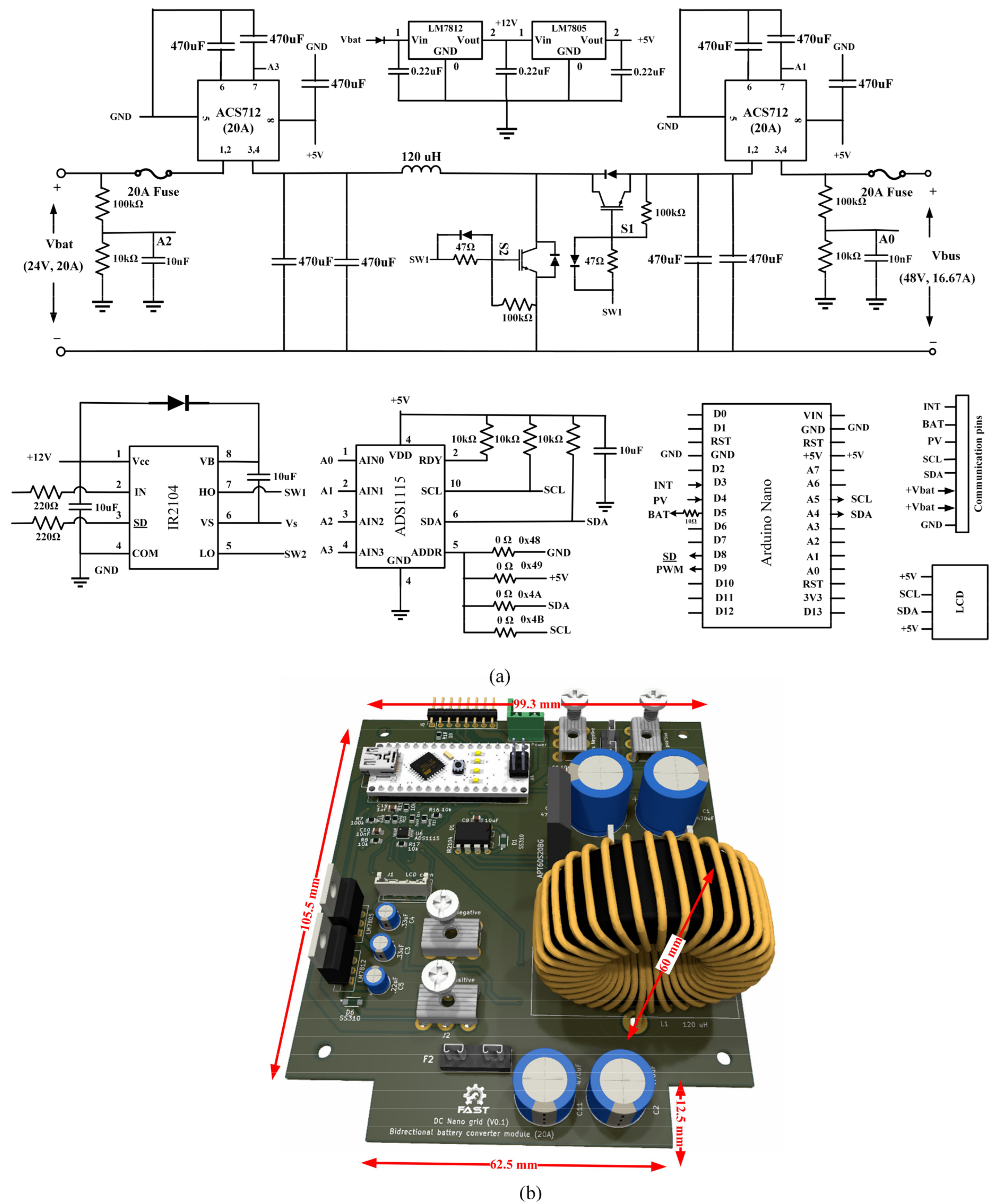
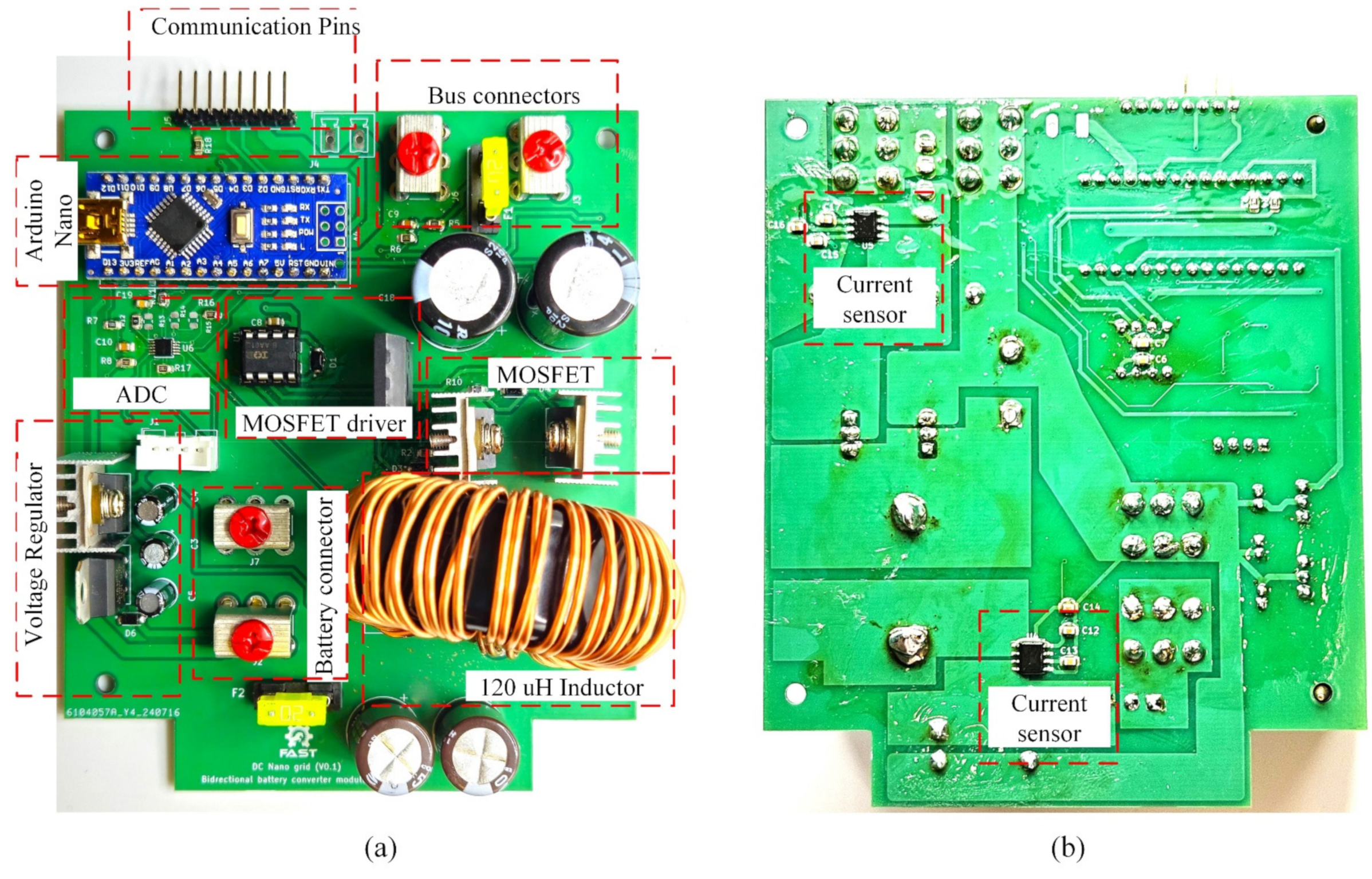
The bidirectional buck-boost converter is designed using two alternately switched MOSFETs and one reverse parallel diode to reduce stress on the lower-side MOSFET when it is switched off. The duty ratio of the switching pulse is controlled to regulate both the current and the direction of current flow. With the battery connected to the source terminal of the high-side MOSFET, an IR 2104 MOSFET driver with a bootstrap capacitor keeps the gate voltage above the battery voltage during switching. The Arduino Nano manages the switching pulse and controls the charging and discharging current by monitoring four parameters: battery voltage, charging current, bus voltage, and discharge current, all through a 16-bit ADS1115 analog-to-digital converter. The ADC can have four unique addresses, which allows multiple battery converters to be connected and share data using the same I2C bus.
The Arduino code limits the discharge current to the maximum allowable battery discharge rate. During charging, two modes are utilized for the lithium battery until the state of charge (SOC) reaches 95%. Initially, the controller charges the battery at the current supplied by the MPPT, provided it is below the maximum charging current of the battery. Once the SOC is 95%, the charging mode switches to constant voltage mode, charging the battery at a constant voltage with lower current. At this point, the digital pin dedicated to the battery signal (BS) is set high, signaling the MPPT to switch from the MPPT mode to the bus control mode. The schematic and PCB of the bidirectional converter are shown in Figure 6. The assembled battery converter with components on the board is shown in Figure 7.

2.4.2. PV Boost Converter Design

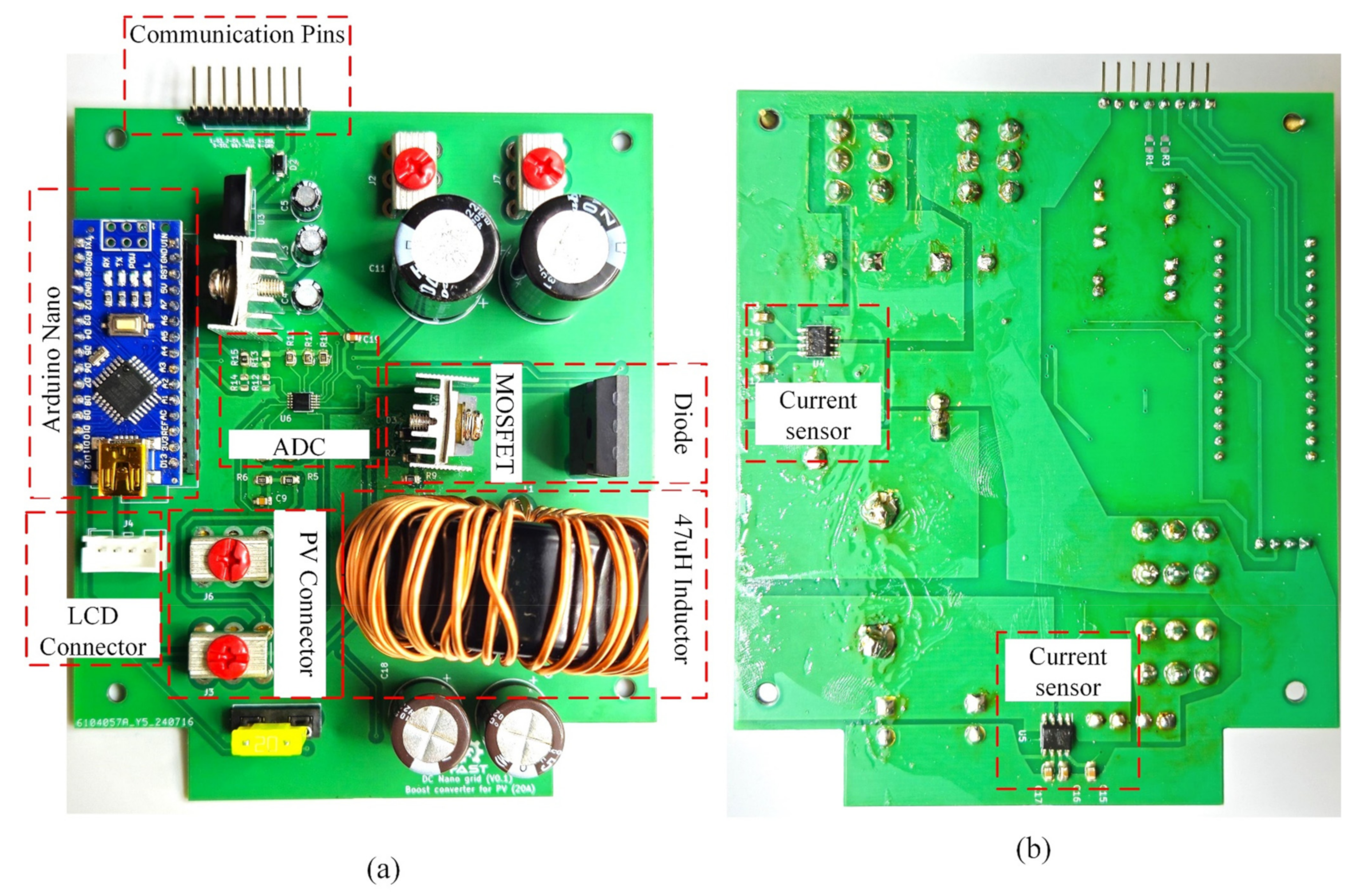
The boost converter for the PV system is rated at 800 W, with an input voltage range of 15–40 V, and it boosts the voltage to 48 V. The converter is designed with one low-side MOSFET and a diode to allow for the current flow from the PV to the bus. The pulse generated by the Arduino Nano is sufficient to drive the MOSFET. The system measures PV voltage, PV current, bus voltage, and current supplied to the bus using an ADS1115 16-bit ADC. The ADS1115 has four unique addresses, allowing multiple PV and battery converters to connect, each with a unique ADC address, as they all share the same I2C bus. Jumper resistor connections (R13, R15, R14, and R12) provide the four unique addresses of 0 × 48, 0 × 49, 0 × 4A, and 0 × 4B shown in Figure 8. The PV converter can be excluded from the I2C bus to prevent frequent interruptions by the master controller for data acquisition, with jumper resistors to isolate from the I2C bus. Instead, an OLED display can be connected to the PV converter to show local vital information, while overall critical system status is shared through the digital pin.
The PV converter operates in two different modes based on the BS signal provided by the battery. When the battery is in the constant current (CC) mode, the PV operates in the MPPT mode. The rest of the time, it operates in the bus control mode. The components and the assembled boost converter are shown in Figure 9.

2.4.3. Buck Converter Design

To serve loads of different voltage levels, a DC–DC converter was designed using an open-source Arduino Nano and a PI controller to regulate the output voltage according to a predefined reference. A synchronous buck converter, utilizing two CSD19533KCS MOSFETs (100 V, 100 A) [71], is used instead of a conventional buck converter to reduce power loss and improve efficiency, which is achieved due to the replacement of the power diode in a conventional buck converter with a low-side MOSFET [72]. The IR2104 MOSFET driver IC provides complementary pulse width modulation (PWM) pulses to both the low-side and high-side MOSFETs, with a 10 μF bootstrap capacitor included in the driver circuit.
Three different voltage-level load converters can be implemented using the same PCB, requiring only the specific inductor for each converter level as previously calculated. Additionally, the master controller can stop the buck converter from supplying the load either by sending a signal through I2C or by raising the INT pin high. The buck converter schematic and 3D rendering are shown in Figure 10 and the PCBs are shown in Figure 11.

2.4.4. Master Controller Design

In the nanogrid system, all converters and the master controller share the same I2C bus for inter-converter communication. Both the PV and battery converters use ADS1115 ADCs for local measurements on this I2C bus. To prevent interruptions and conflicts, the PV converter, which continuously monitors current and voltage and adjusts switch pulses in MPPT mode, is isolated from the I2C bus prioritizing local measurement. Consequently, the battery converter, load converter, and master controller use the I2C bus, while the PV converter displays its status on its own OLED.
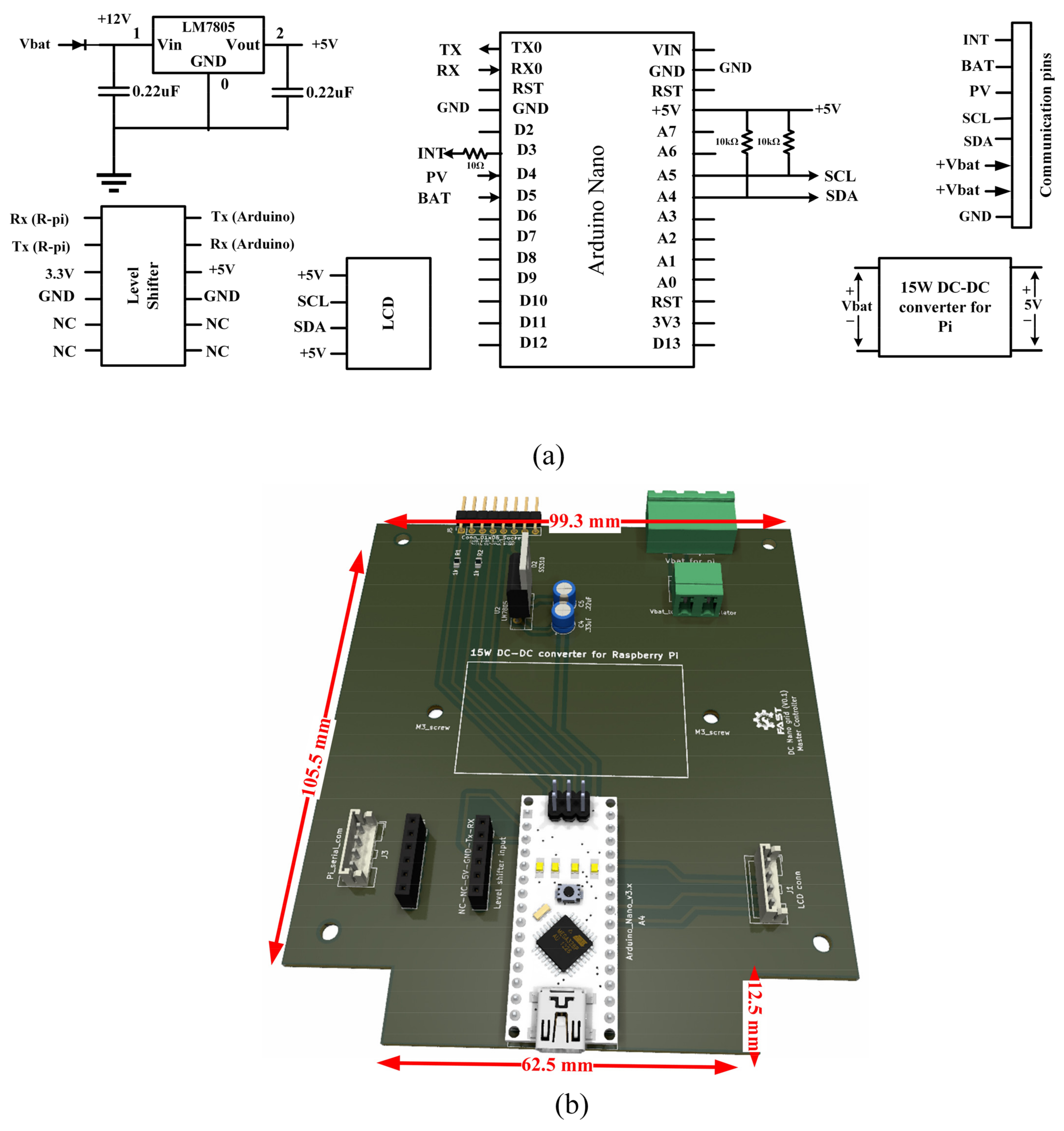
The shared digital pins are always connected to each converter to change their mode of operation. The master controller simultaneously requests voltage, current, and battery SOC data from the battery and load converters. The corresponding converters send back the data, which the master controller then combines sequentially and serially prints to the Raspberry Pi-based GUI and data logger. The circuit and the PCB design of the master controller are shown in Figure 12 and Figure 13.

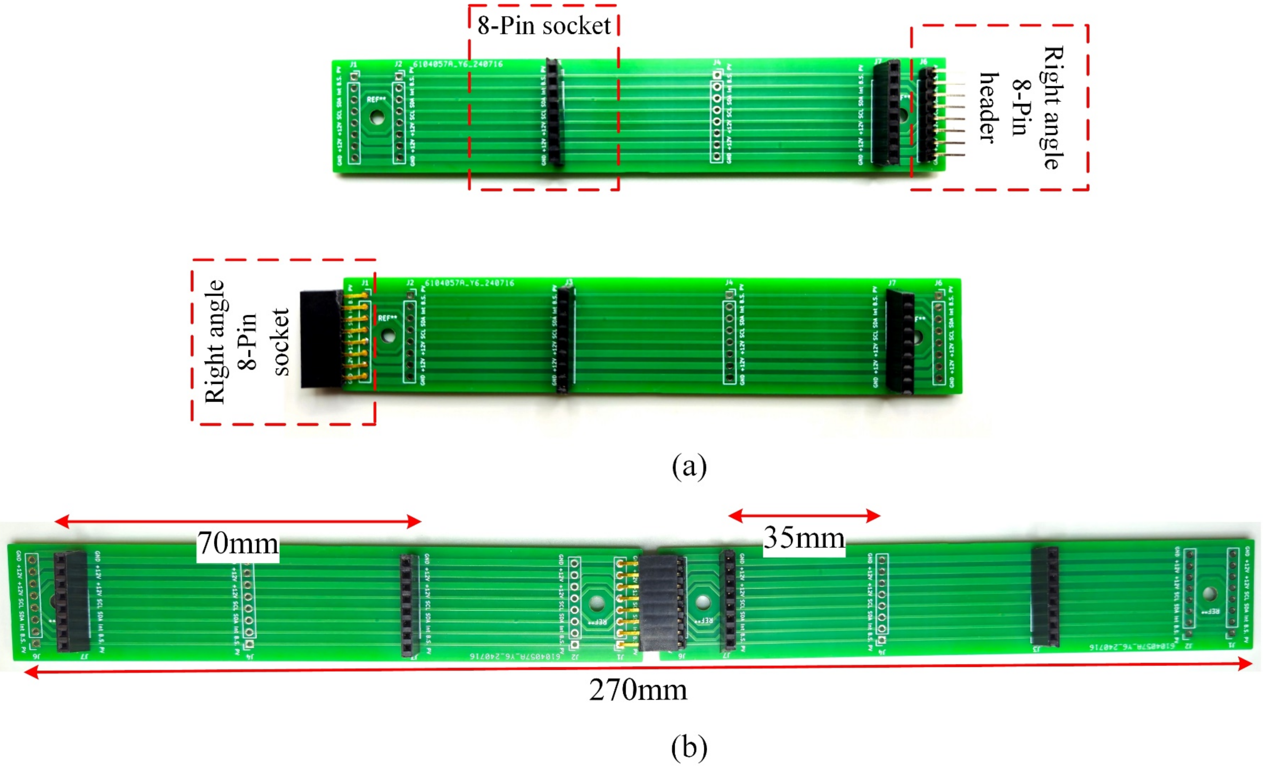
2.4.5. Communication Bus

The communication bus comprises 8 lines used for I2C communication, shared digital pins, and power supply (+12 V, GND) shown in Figure 14. It features an 8-pin socket to interface with the pin headers of the converters and master controller, facilitating information exchange among the converters and the master controller and function of each trace is provided in Table 4. The bus is 25 mm in height and is placed inside the DIN rail where the converters communication pins clip in. Pin sockets are spaced 35 mm apart, and two communication buses can be interconnected to cover the full length of the DIN rail, as shown in Figure 15.

2.4.6. Inductor Design

For designing the inductors of various converters, each handling a peak current of approximately 20–24 A, the toroidal inductor core 0077443A7 from Magnetics (Pittsburgh, PA, USA) is used. This core has an outer diameter of 46.74 mm and a width of 18.03 mm, with a relative magnetic permeability of 75 and an inductance factor of 169 nH per turn. The design parameters for the 47 μH, 120 μH, and 68 μH inductors are summarized in Table 5.

2.5. Bill of Materials

The bill of materials for all subcomponents is listed in a document uploaded in the OSF repository. The summary of the total cost for each subsystem is shown in Table 6 and the total cost of the system is CAD 379. Approximately 40% of the total system cost is attributed to the monitoring and data logging system. Without this component, the total hardware cost is reduced to around CAD 220.

2.6. Arduino Codes and GUI

Each converter and the master Arduino have separate codes, as detailed in Table 7. In addition to the pre-installed libraries in the Arduino IDE, the SSD1306 library for the OLED display and the ADS1115 library for the 16-bit ADC must also be installed. At the start of the code, the PWM switching frequency is selected, and the OLED and ADC are initialized. Except for the master controller, all Arduino code follows a similar structure: measuring circuit parameters using the ADC, averaging three consecutive measurements for accuracy, and then adjusting the PWM duty cycle based on current and voltage measurements to control the converter. When the master requests data from a converter, it interrupts the ongoing operation to transmit the local parameters in a string format. Consequently, the master controller cyclically requests each converter every three seconds. Upon receiving the complete set of data from all converters in a string format, the master concatenates these strings and transmits them as a single unified string, with the length corresponding to the aggregate length of the data from each individual converter.
To avoid interruption from the ADC and OLED display, the firmware must be uploaded to the Arduino before it is placed on the board for the first time. Each converter is assigned a different slave address, defined in the wire setup before initiating transmission, to communicate with the master. If more than one converter of the same type is present in the system, each must be assigned a different wire address.

2.7. Interface and GUI

All converter controllers utilize Arduino Nano processors, and the EMS is also implemented on an Arduino Nano serving as the master processor. This master processor communicates with the other Arduino Nanos within the DC nanogrid using an I2C communication protocol, while the master controller only communicates with Raspberry Pi using a serial communication protocol. To display the status and voltage/current levels of each converter, a Raspberry Pi (Cambridge, UK) with a 7-inch display has been integrated into the system as a separate module. This display module, along with the master Arduino, functions as the central control unit of the entire DC nanogrid.
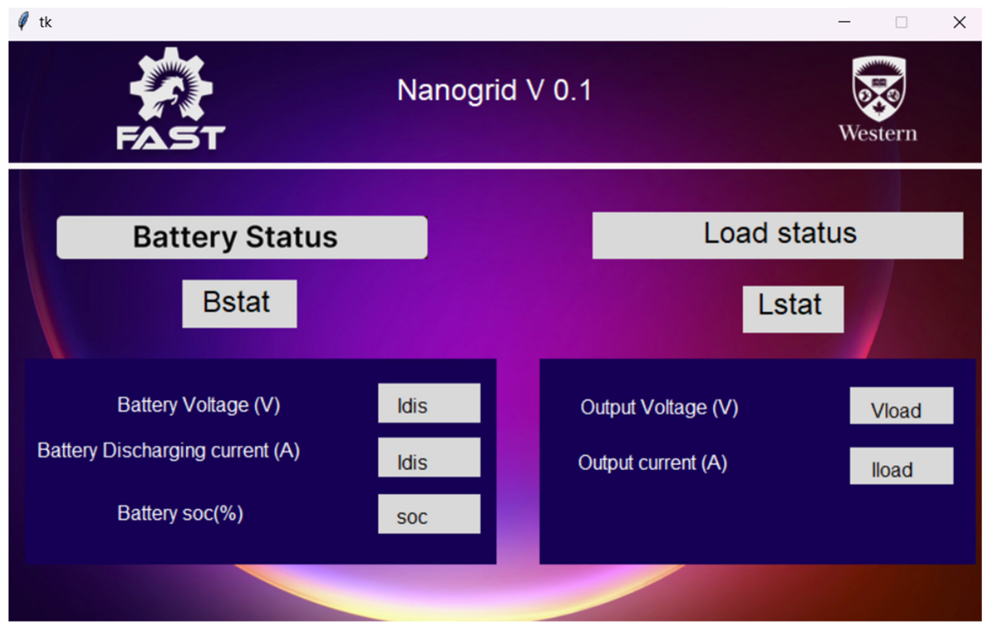
The graphical user interface (GUI) for the nanogrid system operates by receiving real-time data from a master Arduino via serial communication. These data, transmitted through a USB connection at a baud rate of 9600, are processed by a Raspberry Pi running a Python script using the Tkinter library. Currently, with only the battery converter and one load converter connected, the GUI is designed to display their statuses exclusively, including battery voltage, state of charge (SOC), battery discharging current, output voltage of load converter, and output current shown in Figure 16.
The Python script continuously reads the incoming serial data in a separate thread, ensuring that the GUI remains responsive. The data ear processed, and specific values are extracted and updated on the display in real time. For instance, the battery status and load status are dynamically updated based on the current and voltage readings. The GUI, developed using the Tkinter library in python, provides a user-friendly interface with clear visual indicators, making it easier to monitor the nanogrid’s performance in real time. This setup enhances the reliability and efficiency of the DC nanogrid system by offering real-time monitoring and control. This GUI is open source and can be modified as needed. As this is the initial version of the GUI, it can be easily modified in the future to send commands to the master Arduino for controlling the DC nanogrid.

2.8. Step-by-Step Integration and Commissioning Process

The installation process and guidelines are as follows:
  • The design and assembly process of the frame and the converters encloser is given in Appendix A.
  • After the converter and the frame are designed, attach the master controller to the frame. This is the only unit that does not require connections to the bus bar, and there should only be one master controller present in a DC nanogrid.
  • Attach the PV and battery modules to the system one by one. For systems with multiple PV and battery modules, alternate the installation sequence between PV and battery to maintain consistent DC resistance across all modules.
  • Attach the buck converter module and inverters module (if any) to the system according to the load requirements.
  • Sequentially turn on all the battery switches. This action will power on the master controller and all connected modules along with the Raspberry Pi display. Next, connect the PV panels to the PV converter, and finally, connect the loads to the system.
  • For shutdown, follow the reverse order of the installation process.

3. Results

3.1. MATLAB Simulink Results

To verify the performance of the EMS and stability of the nanogrid by simulation, two different cases were analyzed: (1) variation in PV generation and (2) variation in load.
  • Case 1: Variation in irradiance
In case 1, the nanogrid operates under varying irradiance conditions, which causes variations in the PV generation. Initially, the solar irradiation is considered 1000 W/m2, the ambient temperature is 300 K, and the maximum PV output is 656 W. Thus, all the DC loads (total DC load power is 380 W) with different voltage levels, listed in Table 8, are powered by the PV and the remaining power is delivered to the battery.
At the 1.0 s, there was a transition in irradiance to 700 W/m2, and the PV output decreased to 464 W, yet the system continued to operate with a surplus of power. During this period, the battery was charged with an excess power of 84 W. Subsequently, at 2.0 s, the irradiance was further reduced to 300 W/m2. The PV power output decreased to 198 W, causing the system to enter a power deficit mode. However, the DC bus voltage remained steady at 48 V throughout the simulation period, as shown in Figure 17. The deficit power is supplied by the battery with a discharging power of around 200 W.
  • Case 2: Variation of load
Variation of the total load in the system is the common source of instability in any system. But having tuned PI controllers in the system, the instability is avoided, which is already verified in impedance scanning, Now, in the time domain simulation in Figure 18, the DC bus voltage is stable when the DC loads vary according to Table 9. The PV generated power is considered constant throughout the full simulation period at 380 W under 500 W/m2 irradiance and 300 K temperature. Initially, the system is in the power deficit mode since PLoad > PPV. And a slight decrease in DC loads to 400 W after 1 s results in a decrease in power supplied by the battery. The system, however, remains in the power deficit mode. Finally, at 2 s, the significant decrease in load to 200 W sends the system into power surplus mode, and now the system charges the battery with 180 W.
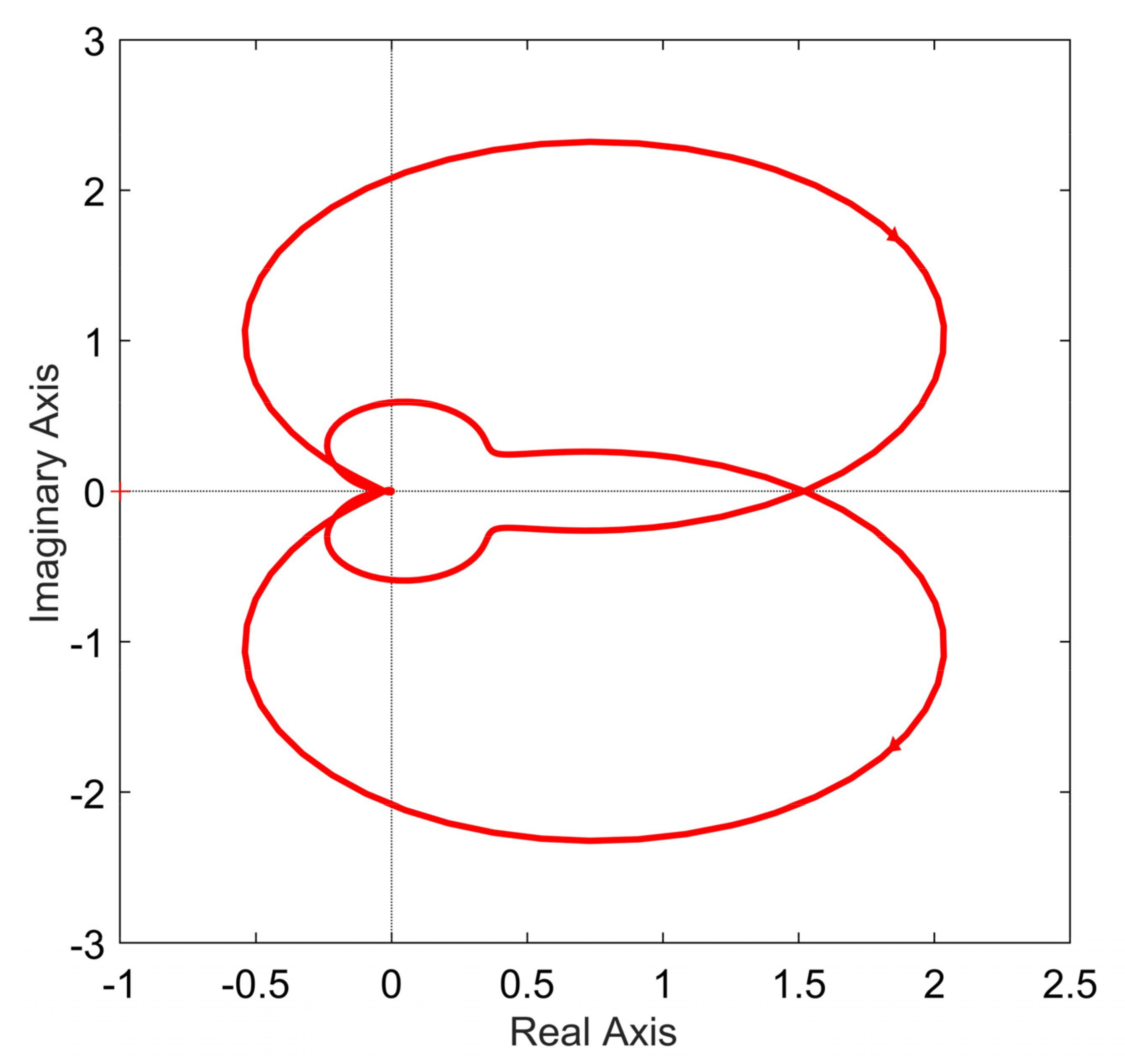
These two cases and simulation results indicate that the designed nanogrid is stable, and any instability can be mitigated by the converters within the system. Alongside the time domain simulation, impedance scanning has been used extensively with the Nyquist plot to analyze the small signal stability of interconnected systems [73] and serves as a valuable tool for assessing the stability of converter-based interconnected systems by considering the input-output characteristics (impedance) of each subsystem [74]. To evaluate the stability, the overall nanogrid system is first split into source side impedance ZS and load side impedance ZL. According to the Nyquist theory, a system is stable if the Nyquist plot of Z S Z L curve does not encircle (−1, 0) point in the negative plane [75,76]. Figure 19 presents the Nyquist plot as a function of frequency, demonstrating a significant separation from the (−1, 0) point. Consequently, it is evident that the system can be deemed stable.

3.2. Final Nanogrid Hardware and Validation Tests

The assembled nanogrid hardware is shown in Figure 20. The PV converter, 24 V load converter, and battery controller are placed in order from the left, all housed in blue enclosures. The master controller in green encloser is positioned on the far right, close to the Raspberry Pi display.

3.3. Supply Voltage Stability of 24 V Load

A 30 W load is connected to the system and subsequently disconnected to evaluate the stability of the supply voltage, as shown in Figure 21. The supply voltage remains stable during the load variation and quickly returns to the reference 24 V after the disconnection.

4. Discussion

While hybrid nanogrids can simultaneously provide both AC and DC power [77], the feasibility and benefits of using a DC distribution network in conjunction with renewable energy sources have already been widely explored and documented [78]. Conventional PV systems mostly use inverters to supply AC power to loads, even though most low-power household loads are DC. In contrast, this nanogrid system is entirely DC and can supply power at different DC levels. For a DC nanogrid network, converters play the most significant role in operating the whole system [79]. Therefore, a general design framework for converters was proposed to ensure reliable steady-state and dynamic responses when various loads are integrated into the system [80]. Even to control modern unidirectional and bidirectional DC–DC converters, several control techniques are implemented and discussed briefly [81]. The development of new converter techniques and control mechanisms remains a significant focus for researchers, who are consistently innovating with new control strategies [82] and converter topologies [83]. For instance, experimental validation of a three-port bidirectional converter was conducted, along with a novel control technique, to ensure high reliability when integrated with a solar PV system [84]. Even the interconnection between two DC nanogrids to exchange power and communication between them is demonstrated and explained [85].
This paper differentiates itself by not extensively discussing new control mechanisms or converter designs for DC nanogrids. Instead, it focuses on the comprehensive setup of a DC nanogrid. This includes maximizing power extraction from solar PV, maintaining a stable DC bus voltage, and ensuring the proper operation of the battery system to supply power to appliances at their required voltage levels. A key aspect of its uniqueness is its modularity and the device version of the DC distribution network system. This represents the first-ever nanogrid that incorporates all the features of a complete DC nanogrid in a modular, user-friendly, plug-and-play hardware design. It is designed to be easily assembled and operated by users, making it accessible for DIY applications [86] and enhancing its practicality and flexibility. The hardware implementation is completed using an open-source design. Later, the bus voltage stability and the supply voltage quality of the hardware are also verified.
This hardware modular DC nanogrid is distinguished by its advanced design architecture and targeted application. Unlike commercial inverter-based portable solar power stations [87], which can integrate PV panels for charging but are typically expensive, proprietary, and non-expandable, this nanogrid offers a flexible and scalable solution. While commercial systems primarily supply AC power, with limited DC output available for specific loads by available USB ports, the modular DC nanogrid is designed for optimized DC power delivery, enhancing efficiency and compatibility with various DC loads.
An alternative DC nanogrid setup can be constructed using commercial proprietary MPPTs and DC–DC converters connected to a common bus bar, solely for supplying DC power to a dedicated load. In this configuration, the bus voltage will be determined by the battery voltage as the battery is directly connected. However, 20 A system of this kind, including a monitoring system, can cost over CAD 1600 while sacrificing key features such as modularity, compact size, and compatibility [88].
Additionally, for a compact nanogrid setup, there are no MPPTs available that are compatible with DIN rails. While there are DC–DC converters, such as a 24 V, 20 A [89] converter operating with a 48 V input, these alone can cost around CAD 300, which is more expensive than the entire nanogrid system. Also, the benefit of the open-source hardware is the adaptation of this nanogrid using material from local vendors, and it provides the opportunity to modify the device quite easily according to users’ requirements. Its modular design allows for easy integration into a frame or electrical box. Single households, vehicles such as ambulances, mini-clinics, and camps can be powered using the nanogrid setup, with the design facilitating easy modifications to integrate new loads and batteries. While this setup introduces a novel strategy for making PV systems modular and more accessible, further improvements in the GUI and communication system are necessary for the seamless integration of converter modules. Additionally, a better communication strategy is needed to enable the PV converter to share data with the master controller without interruption. Implementing a more advanced MPPT algorithm could also help reduce the impact of partial shading. Currently, the converters are connected to the bus bar using wires, which disrupts seamless integration, but incorporating bus bar clips will make the process easier. Being open source will allow for modifications by the user such as disconnecting low-priority loads when the generation capability is inadequate [90].

5. Conclusions

The novel open-source modular DC nanogrid presented in this paper is the first hardware implementation of a plug-and-play device that is easily adaptable, expandable, and customizable at different voltage and power levels. Transforming the nanogrid from a distribution network to a device is not only novel but makes it suitable for various user-specific applications, such as remotely supplying power to camp vehicles, campsites, emergency vehicles like ambulances, and small houses lacking grid electricity. The modular DC nanogrid includes all the features available in a DC distribution network, including intercommunication of each converter using a master–slave protocol. It also exhibits additional features, such as data logging, which enhances user experience and promotes the use of DC grid systems. This approach not only makes the system more user-friendly but also differentiates it from traditional PV systems, promoting the adoption of DC grid systems as a modular device. The cost of each converter module ranges from CAD 50 to CAD 70, with up to 40% of the total cost attributed to the monitoring system, a cost that remains constant even for larger systems. Although there is no similar approach to designing modular PV systems in the existing literature or commercial products, the total cost of the open-source nanogrid is promising and significantly lower compared with alternative commercial solutions for DC loads. Additionally, any voltage variations due to load changes are quickly stabilized, typically within less than 5 s, making the system promising for future adoption.
The converter technologies, maximum power point tracking (MPPT), and battery charge controller technologies are well-established products that are used on conventional PV systems. The novelty and user-friendly features of the proposed nanogrid system are as follows:
Open-source hardware implementation: Implementing these technologies using open-source hardware and then forming a nanogrid in a modular and adaptable manner is completely novel.
Modular device design: Creating the nanogrid as a device with interconnection and control techniques makes it distinct from conventional PV systems.
User-friendly features: Additional features, such as data logging, enhance user experience and promote the use of DC grid systems. This approach not only makes the system more user-friendly but also differentiates it from traditional PV systems, promoting the adoption of DC grid systems.

Author Contributions

Conceptualization, J.M.P.; methodology, M.M.R., S.K. and J.M.P.; software, M.M.R.; validation, M.M.R.; formal analysis, M.M.R., S.K. and J.M.P.; investigation, M.M.R.; resources, J.M.P.; data curation, M.M.R., S.K. and J.M.P.; writing—original draft preparation, M.M.R., S.K. and J.M.P.; writing—review and editing, M.M.R., S.K. and J.M.P.; visualization, M.M.R. and S.K.; supervision, J.M.P.; project administration, J.M.P.; funding acquisition, J.M.P. All authors have read and agreed to the published version of the manuscript.

Funding

This research was funded by the Thompson Endowment and the Natural Sciences and Engineering Research Council of Canada and the Frugal Biomed Initiative at Western University.

Institutional Review Board Statement

Not applicable.

Informed Consent Statement

Not applicable.

Data Availability Statement

All data are available and the design files are at https://osf.io/73yf5/.

Conflicts of Interest

The authors declare no conflicts of interest. The funders had no role in the design of the study; in the collection, analyses, or interpretation of data; in the writing of the manuscript; or in the decision to publish the results.

Appendix A

Appendix A.1. Integration of Converters

To house the converters and to interconnect them, an open-source frame is designed to facilitate modular plugging of the converters onto the frame’s DIN rail. A display with a Raspberry Pi is used for data monitoring and logging. The converters and the master controller are also housed in individual enclosures. Both the converters and the frame support the installation of the system.

Appendix A.1.1. DC Nanogrid Frame Design

The parts required for assembling the frame are listed in Table A1 along with the open-source repository of the files. All custom components can be 3D printed on a RepRap class- [91,92] open-source 3D printer. Components were printed using polylactic acid (PLA) filament in Prusa MK3 print using print settings given in Table A2.
Table A1. The 3D-printed components required for assembly of the frame of the DC nanogrid—all licensed by CERN OHL-S 2.0.
Parts NameQuantityFile TypeLocation of File
Sliding corner bracket8STEP/stlhttps://osf.io/73yf5/
Corner bracket8STEP/stlhttps://osf.io/73yf5/
Holder for DIN rail2STEP/stlhttps://osf.io/73yf5/
Holder for bus bar2STEP/stlhttps://osf.io/73yf5/
Case for display1STEP/stlhttps://osf.io/73yf5/
Encloser for Raspberry pi1STEP/stlhttps://osf.io/73yf5/
Raspberry pi holder1STEP/stlhttps://osf.io/73yf5/
The printing parameters are summarized in Table A2 and can be printed on any RepRap class 3D printer.
Table A2. Three-dimensional printing parameters.
ParameterValue
FilamentPLA
Layer height0.3 mm
Initial layer height0.2 mm
Infill density15%
Printing temperature210 °C
Build plate temperature60 °C
Print speed60 mm/s
Travel speed175 mm/s
The frame is designed as an alternative to placing all components inside an electrical box. The parts needed are shown in Figure A1. It will hold three converters and a master controller box, with dimensions of 420 mm in length and 390 mm in height. These dimensions can be adjusted as needed. Two pieces of 350 mm aluminum extrusion bars serve as stands. To support them, three pieces of 80 mm long aluminum extrusion are used per stand, totaling six pieces. A 420 mm long aluminum extrusion bar connects the two stands together. Two 410 mm bus bars are cut from a 1 m long bus bar. There is a 410 mm long DIN rail to accommodate the converters. Four types of corner brackets and holders are used in this design process, as detailed in Table A1. The design steps are also mentioned in Figure A2. A case and holder are made for the display connected to the Raspberry Pi 4b for data monitoring and also connected to one of the bars of the frame.
To assemble the frame to accommodate the DIN rail, bus bars, and monitoring system, the following steps are followed:
  • The stands were assembled using the 350 mm aluminum extrusions and 80 mm support pieces first.
  • The 420 mm aluminum extrusion was attached to the stands to form the frame.
  • The 410 mm bus bars and DIN rail were installed within the frame.
  • A case and holder for the display connected to the Raspberry Pi 4b for data monitoring were created and attached to one of the bars of the frame.
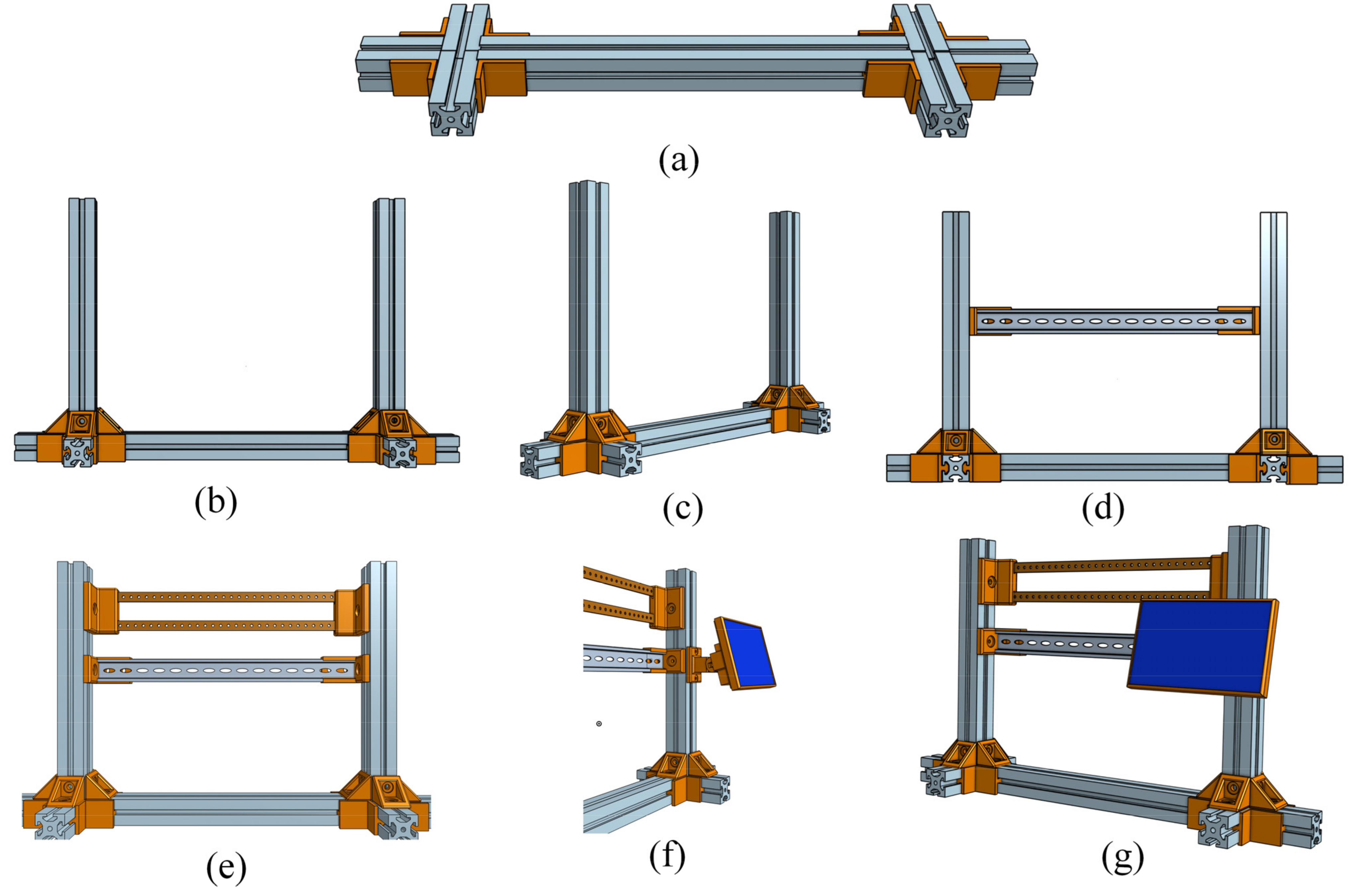
Figure A2a–g provides detailed design steps and the types of corner brackets and holders used and Figure A3 shows the assembled frame.
Figure A1. Parts required for assembly of frame.
Technologies 12 00167 g0a1
Figure A2. Assembly process of the frame (a) Base Assembly, (b) Attaching vertical bars, (c) Side view of vertical frame, (d) Attaching DIN rail, (e) Mounting bus bars, (f) Mounting the display and (g) Final assembly with mounted display.
Technologies 12 00167 g0a2
Figure A3. Assembled frame.
Technologies 12 00167 g0a3

Appendix A.1.2. Converters Encloser Design

Each converter and master controller have an enclosure that is adequately ventilated. The enclosures are designed with the same shape, but their widths vary based on the converter module, as not all converters have the same width or features. Each module has a clip to connect to the DIN rail, with pockets for passing wires to the bus bar and communication ports. The front panel of the enclosure features different elements based on the module: the boost converter has its own display, and the master controller has a port to connect the USB from the Raspberry Pi for serial data sharing and power supply. The STEP and STL files for all the enclosures are available in the repository listed in the following Table A3. Rendered images of the master controller are shown in Figure A4. All the enclosures were printed using a 0.6 mm nozzle at a 0.3 mm layer height with 15% infill, utilizing PLA filament.
Figure A4. Rendered 3D image of master controller encloser (a) Exploded view showing the PCB, (b) Rear view and (c) Front view.
Technologies 12 00167 g0a4
Table A3. The 3D-printed components required for assembly of converters and master controller—all licensed by CERN OHL-S 2.0.
Parts NameQuantityFile TypeLocation of File
Buck converter encloser1STEP/stlhttps://osf.io/73yf5/
Buck converter lid1STEP/stlhttps://osf.io/73yf5/
Boost converter encloser1STEP/stlhttps://osf.io/73yf5/
Boost converter lid1STEP/stlhttps://osf.io/73yf5/
Bidirectional converter encloser1STEP/stlhttps://osf.io/73yf5/
Bidirectional converter lid1STEP/stlhttps://osf.io/73yf5/
Master controller encloser1STEP/stlhttps://osf.io/73yf5/
Master controller lid1STEP/stlhttps://osf.io/73yf5/

Appendix A.1.3. Final Assembly

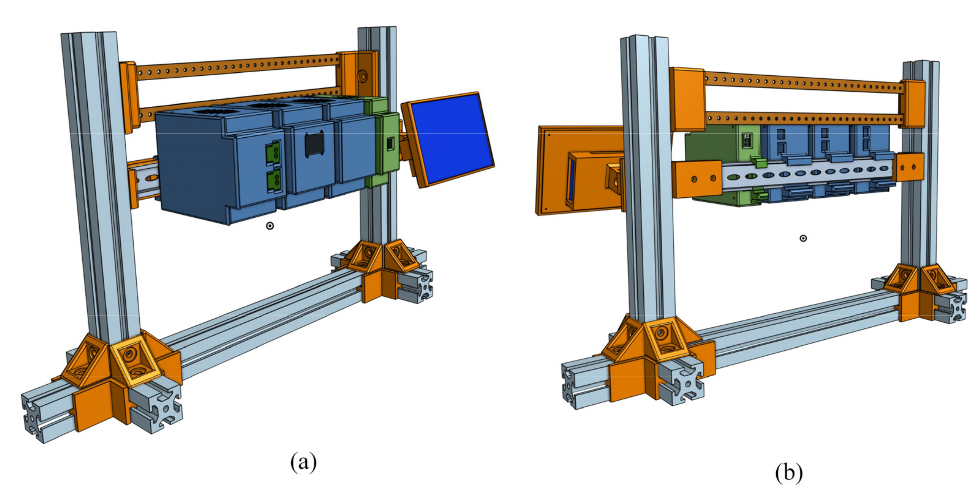
After the enclosures are printed, the PCBs are placed inside, the wiring is completed, and the communication pins are attached to the communication bus in all the converters before placing them on the DIN rail. Once the converters are secured in the DIN rails, the necessary connections between all the positive and negative terminals of the converters and the corresponding bus bar are made. The battery converter also has a direct battery power supply port to the master, designated for the Raspberry Pi converter. After all the interconnections are completed, the power supply and USB connection between the master Arduino and Raspberry Pi are established, as shown in Figure A5.
Figure A5. Final assembly rendered 3D image of the nanogrid system (a) Front view and (b) Rear view.
Technologies 12 00167 g0a5

References

  1. Zhou, X.; Guo, T.; Ma, Y. An Overview on Microgrid Technology. In Proceedings of the 2015 IEEE International Conference on Mechatronics and Automation (ICMA), Beijing, China, 2–5 August 2015; pp. 76–81. [Google Scholar]
  2. Nordman, B.; Christensen, K. DC Local Power Distribution with Microgrids and Nanogrids. In Proceedings of the 2015 IEEE 1st International Conference on DC Microgrids (ICDCM), Atlanta, GA, USA, 7–10 June 2015; pp. 199–204. [Google Scholar]
  3. Schonbergerschonberger, J.; Duke, R.; Round, S.D. DC-Bus Signaling: A Distributed Control Strategy for a Hybrid Renewable Nanogrid. IEEE Trans. Ind. Electron. 2006, 53, 1453–1460. [Google Scholar] [CrossRef]
  4. Nag, S.; Adda, R.; Ray, O.; Mishra, S. Current-Fed Switched Inverter Based Hybrid Topology for DC Nanogrid Application. In Proceedings of the IECON 2013—39th Annual Conference of the IEEE Industrial Electronics Society, Vienna, Austria, 10–13 November 2013; pp. 7146–7151. [Google Scholar]
  5. Pearce, J.M. Photovoltaics—A Path to Sustainable Futures. Futures 2002, 34, 663–674. [Google Scholar] [CrossRef]
  6. Tsuma, M.; Kibaara, S. A Review of Levelized Cost of Electricity for Photovoltaic Systems Combining with Their Environmental Impacts. In Proceedings of the Sustainable Research and Innovation Conference, Juja, Kenya, 8–10 May 2019; pp. 220–225. [Google Scholar]
  7. Zhang, P.; Li, W.; Li, S.; Wang, Y.; Xiao, W. Reliability Assessment of Photovoltaic Power Systems: Review of Current Status and Future Perspectives. Appl. Energy 2013, 104, 822–833. [Google Scholar] [CrossRef]
  8. Şen, Z. Solar Energy in Progress and Future Research Trends. Prog. Energy Combust. Sci. 2004, 30, 367–416. [Google Scholar] [CrossRef]
  9. Vives, M.V.; Chamorro, H.R.; Ortiz-Villalba, D.; Jiménez, F.; Gonzalez-Longatt, F.M.; Jimenez-Estevez, G.; Guerrero, J.; Cadena, A.; Sood, V.K. Nanogrids: Good Practices and Challenges in the Projects in Colombia. In Microgrids for Rural Areas; Institution of Engineering and Technology: London, UK, 2020; pp. 421–446. [Google Scholar]
  10. Assis, F.A.; Coelho, F.C.R.; Castro, J.F.C.; Donadon, A.R.; Roncolatto, R.A.; Rosas, P.A.C.; Andrade, V.E.M.S.; Bento, R.G.; Silva, L.C.P.; Cypriano, J.G.I.; et al. Assessment of Regulatory and Market Challenges in the Economic Feasibility of a Nanogrid: A Brazilian Case. Energies 2024, 17, 341. [Google Scholar] [CrossRef]
  11. Breyer, C. Low-Cost Solar Power Enables a Sustainable Energy Industry System. Proc. Natl. Acad. Sci. USA 2021, 118, e2116940118. [Google Scholar] [CrossRef]
  12. Staff, C.B. Solar Is Now ‘Cheapest Electricity in History’, Confirms IEA. Available online: https://www.carbonbrief.org/solar-is-now-cheapest-electricity-in-history-confirms-iea/ (accessed on 28 July 2024).
  13. Sajeeb, M.M.H.; Rahman, A.; Arif, S. Feasibility Analysis of Solar DC Nano Grid for off Grid Rural Bangladesh. In Proceedings of the 2015 3rd International Conference on Green Energy and Technology (ICGET), Dhaka, Bangladesh, 11–12 September 2015; pp. 1–5. [Google Scholar]
  14. Khan, M.R.; Brown, E.D. DC Nanogrids: A Low Cost PV Based Solution for Livelihood Enhancement for Rural Bangladesh. In Proceedings of the 2014 3rd International Conference on the Developments in Renewable Energy Technology (ICDRET), Dhaka, Bangladesh, 29–31 May 2014; pp. 1–5. [Google Scholar]
  15. Hamatwi, E.; Davidson, I.E.; Agee, J.; Venayagamoorthy, G. Model of a Hybrid Distributed Generation System for a DC Nano-Grid. In Proceedings of the 2016 Clemson University Power Systems Conference (PSC), Clemson, SC, USA, 8–11 March 2016; pp. 1–8. [Google Scholar]
  16. Dahiru, A.T.; Tan, C.W. Optimal Sizing and Techno-Economic Analysis of Grid-Connected Nanogrid for Tropical Climates of the Savannah. Sustain. Cities Soc. 2020, 52, 101824. [Google Scholar] [CrossRef]
  17. Shwehdi, M.H.; Mohamed, S.R. Proposed Smart DC Nano-Grid for Green Buildings—A Reflective View. In Proceedings of the 2014 International Conference on Renewable Energy Research and Application (ICRERA), Milwaukee, WI, USA, 19–22 October 2014; pp. 765–769. [Google Scholar]
  18. Mishra, S.; Ray, O. Advances in Nanogrid Technology and Its Integration into Rural Electrification in India. In Proceedings of the 2014 International Power Electronics Conference (IPEC-Hiroshima 2014—ECCE ASIA), Hiroshima, Japan, 18–21 May 2014; pp. 2707–2713. [Google Scholar]
  19. Kinn, M.C. Proposed Components for the Design of a Smart Nano-Grid for a Domestic Electrical System That Operates at below 50V DC. In Proceedings of the 2011 2nd IEEE PES International Conference and Exhibition on Innovative Smart Grid Technologies, Manchester, UK, 5–7 December 2011; pp. 1–7. [Google Scholar]
  20. Taufik, T.; Muscarella, M. Development of DC House Prototypes as Demonstration Sites for an Alternate Solution to Rural Electrification. In Proceedings of the 2016 6th International Annual Engineering Seminar (InAES), Yogyakarta, Indonesia, 1–3 August 2016; pp. 262–265. [Google Scholar]
  21. Khan, S.; Rahman, M.M. Design and Simulation of Solar DC Nano Grid System from Bangladesh Perspective. In Proceedings of the 2021 International Conference on Automation, Control and Mechatronics for Industry 4.0 (ACMI), Rajshahi, Bangladesh, 8–9 July 2021; pp. 1–6. [Google Scholar]
  22. Joseph, S.C.; Ashok, S.; Dhanesh, P.R. Low Voltage Direct Current (LVDC) Nanogrid for Home Application. In Proceedings of the 2017 IEEE Region 10 Symposium (TENSYMP), Cochin, India, 14–16 July 2017; pp. 1–5. [Google Scholar]
  23. Tudu, B.; Mandal, K.K.; Chakraborty, N. Optimal Design and Development of PV-Wind-Battery Based Nano-Grid System: A Field-on-Laboratory Demonstration. Front. Energy 2019, 13, 269–283. [Google Scholar] [CrossRef]
  24. Almasri, A.; Al Shabrawi, B.; Sardar, A.; Al Atifi, A.; Al Harbi, A.; Ammous, A. Contribution to the Realization of DC Nano-Grid Including PV Source. In Proceedings of the 2020 Industrial & Systems Engineering Conference (ISEC), Makkah, Saudi Arabia, 9–12 April 2020; pp. 1–5. [Google Scholar]
  25. Cvetkovic, I.; Dong, D.; Zhang, W.; Jiang, L.; Boroyevich, D.; Lee, F.C.; Mattavelli, P. A Testbed for Experimental Validation of a Low-Voltage DC Nanogrid for Buildings. In Proceedings of the 2012 15th International Power Electronics and Motion Control Conference (EPE/PEMC), Novi Sad, Serbia, 4–6 September 2012; pp. LS7c.5-1–LS7c.5-8. [Google Scholar]
  26. Rahman, M.M.; Antonini, G.; Pearce, J. Open-Source DC-DC Converter Enabling Direct Integration of Solar Photovoltaics with Anion Exchange Membrane Electrolyzer for Green Hydrogen Production. Preprints 2024. [Google Scholar] [CrossRef]
  27. Gadzanku, S.; Kramer, A.; Smith, B. An Updated Review of the Solar PV Installation Workforce Literature; National Renewable Energy Laboratory (NREL): Golden, CO, USA, 2023. [Google Scholar] [CrossRef]
  28. Chagas, A.M. Haves and Have Nots Must Find a Better Way: The Case for Open Scientific Hardware. PLoS Biol. 2018, 16, e3000014. [Google Scholar] [CrossRef]
  29. Gibb, A. Building Open Source Hardware: DIY Manufacturing for Hackers and Makers; Addison-Wesley Professional: Boston, MA, USA, 2014; ISBN 978-0-13-337390-5. [Google Scholar]
  30. Rahman, M.M.; Pearce, J. Modular Open Source Solar Photovoltaic-Powered DC Nanogrids with Efficient Energy Management System. Sol. Energy Sustain. Dev. J. 2024, 13, 22–42. [Google Scholar] [CrossRef]
  31. Dong, D.; Cvetkovic, I.; Boroyevich, D.; Zhang, W.; Wang, R.; Mattavelli, P. Grid-Interface Bidirectional Converter for Residential DC Distribution Systems—Part One: High-Density Two-Stage Topology. IEEE Trans. Power Electron. 2013, 28, 1655–1666. [Google Scholar] [CrossRef]
  32. Sudev, V.; Parvathy, S. Switched Boost Inverter Based Dc Nanogrid with Battery and Bi-Directional Converter. In Proceedings of the 2014 International Conference on Circuits, Power and Computing Technologies [ICCPCT-2014], Nagercoil, India, 20–21 March 2014; pp. 461–467. [Google Scholar]
  33. Ganesan, S.I.; Pattabiraman, D.; Govindarajan, R.K.; Rajan, M.; Nagamani, C. Control Scheme for a Bidirectional Converter in a Self-Sustaining Low-Voltage DC Nanogrid. IEEE Trans. Ind. Electron. 2015, 62, 6317–6326. [Google Scholar] [CrossRef]
  34. Sathler, H.H.; Sathler, L.H.; Marcelino, F.L.F.; de Oliveira, T.R.; Seleme, S.I.; Garcia, P.F.D. A Comparative Efficiency Study on Bidirectional Grid Interface Converters Applied to Low Power DC Nanogrids. In Proceedings of the 2017 Brazilian Power Electronics Conference (COBEP), Juiz de Fora, Brazil, 19–22 November 2017; pp. 1–6. [Google Scholar]
  35. Queiroz, F.; Praça, P.; Freitas, A.; Antunes, F. High-Gain Bidirectional DC-DC Converter for Battery Charging in DC Nanogrid of Residential Prossumer. In Proceedings of the 2019 IEEE 15th Brazilian Power Electronics Conference and 5th IEEE Southern Power Electronics Conference (COBEP/SPEC), Santos, Brazil, 1–4 December 2019; pp. 1–6. [Google Scholar]
  36. Goud, P.C.D.; Gupta, R. Solar PV Based Nanogrid Integrated with Battery Energy Storage to Supply Hybrid Residential Loads Using Single-Stage Hybrid Converter. IET Energy Syst. Integr. 2020, 2, 161–169. [Google Scholar] [CrossRef]
  37. Saxena, A.R.; Kulshreshtha, A. A Fourth-Order Bidirectional DC–DC Converter for Interfacing Battery in a Solar -Photovoltaic-Fed Low-Voltage Residential DC Nano-Grid: Design and Analysis. Int. J. Circuit Theory Appl. 2021, 49, 1932–1958. [Google Scholar] [CrossRef]
  38. Bodele, N.J.; Kulkarni, P.S. Modular Battery-Integrated Bidirectional Single-Stage DC–DC Converter for Solar PV Based DC Nano-Grid Application. Sol. Energy 2023, 259, 1–14. [Google Scholar] [CrossRef]
  39. Burmester, D.; Rayudu, R.; Seah, W.; Akinyele, D. A Review of Nanogrid Topologies and Technologies. Renew. Sustain. Energy Rev. 2017, 67, 760–775. [Google Scholar] [CrossRef]
  40. Cairoli, P.; Kondratiev, I.; Dougal, R.A. Controlled Power Sequencing for Fault Protection in DC Nanogrids. In Proceedings of the 2011 International Conference on Clean Electrical Power (ICCEP), Ischia, Italy, 14–16 June 2011; pp. 730–737. [Google Scholar]
  41. Sadabadi, M.S.; Karimi, A.; Karimi, H. Fixed-Order Decentralized/Distributed Control of Islanded Inverter-Interfaced Microgrids. Control Eng. Pract. 2015, 45, 174–193. [Google Scholar] [CrossRef]
  42. Uddin, M.; Mo, H.; Dong, D.; Elsawah, S.; Zhu, J.; Guerrero, J.M. Microgrids: A Review, Outstanding Issues and Future Trends. Energy Strategy Rev. 2023, 49, 101127. [Google Scholar] [CrossRef]
  43. Oberloier, S.; Whisman, N.G.; Hafting, F.; Pearce, J.M. Open Source Framework for a Broadly Expandable and Reconfigurable Data Acquisition and Automation Device (BREAD). HardwareX 2023, 15, e00467. [Google Scholar] [CrossRef]
  44. Schmid, F.; Behrendt, F. Optimal Sizing of Solar Home Systems: Charge Controller Technology and Its Influence on System Design. Sustain. Energy Technol. Assess. 2021, 45, 101198. [Google Scholar] [CrossRef]
  45. Pearce, J.M. Open-Source Lab: How to Build Your Own Hardware and Reduce Research Costs; Elsevier: Amsterdam, The Netherlands, 2013; ISBN 978-0-12-410486-0. [Google Scholar]
  46. Pearce, J.M. Cut Costs with Open-Source Hardware. Nature 2014, 505, 618. [Google Scholar] [CrossRef] [PubMed]
  47. Buitenhuis, A.J.; Pearce, J.M. Open-Source Development of Solar Photovoltaic Technology. Energy Sustain. Dev. 2012, 16, 379–388. [Google Scholar] [CrossRef]
  48. de Arquer Fernández, P.; Fernández Fernández, M.Á.; Carús Candás, J.L.; Arboleya Arboleya, P. An IoT Open Source Platform for Photovoltaic Plants Supervision. Int. J. Electr. Power Energy Syst. 2021, 125, 106540. [Google Scholar] [CrossRef]
  49. González, I.; Portalo, J.M.; Calderón, A.J. Configurable IoT Open-Source Hardware and Software I-V Curve Tracer for Photovoltaic Generators. Sensors 2021, 21, 7650. [Google Scholar] [CrossRef]
  50. Portalo, J.M.; González, I.; Calderón, A.J. Monitoring System for Tracking a PV Generator in an Experimental Smart Microgrid: An Open-Source Solution. Sustainability 2021, 13, 8182. [Google Scholar] [CrossRef]
  51. Santhosh, R.; Sabareesh, S.U.; Aswin, R.; Mahalakshmi, R. Hardware Design of PIC Microcontroller Based Charge Controller and MPPT for the Standalone PV-Battery Charging System. In Proceedings of the 2021 International Conference on Recent Trends on Electronics, Information, Communication & Technology (RTEICT), Xi’an, China, 18–20 August 2021; pp. 172–175. [Google Scholar]
  52. Parandhaman, M.; Annambhotla, L.T.S.; Parthiban, P. Hardware Prototype for Portable Automatic MPPT Solar Charger Using Buck Converter and PSO Technique. In Proceedings of the 2022 IEEE Delhi Section Conference (DELCON), New Delhi, India, 11–13 February 2022; pp. 1–6. [Google Scholar]
  53. Wirateruna, E.S.; Afroni, M.J.; Badri, F. Design of Maximum Power Point Tracking Photovoltaic System Based on Incremental Conductance Algorithm Using Arduino Uno and Boost Converter. Appl. Technol. Comput. Sci. J. 2022, 4, 101–112. [Google Scholar] [CrossRef]
  54. Podder, A.K.; Roy, N.K.; Pota, H.R. MPPT Methods for Solar PV Systems: A Critical Review Based on Tracking Nature. IET Renew. Power Gener. 2019, 13, 1615–1632. [Google Scholar] [CrossRef]
  55. Liu, F.; Duan, S.; Liu, F.; Liu, B.; Kang, Y. A Variable Step Size INC MPPT Method for PV Systems. IEEE Trans. Ind. Electron. 2008, 55, 2622–2628. [Google Scholar] [CrossRef]
  56. Karami, N.; Moubayed, N.; Outbib, R. General Review and Classification of Different MPPT Techniques. Renew. Sustain. Energy Rev. 2017, 68, 1–18. [Google Scholar] [CrossRef]
  57. Rahman, M.M.; Islam, M.S. Artificial Neural Network Based Maximum Power Point Tracking of a Photovoltaic System. In Proceedings of the 2019 3rd International Conference on Electrical, Computer & Telecommunication Engineering (ICECTE), Rajshahi, Bangladesh, 26–28 December 2019; pp. 117–120. [Google Scholar]
  58. Rahman, M.M.; Islam, M.S. PSO and ANN Based Hybrid MPPT Algorithm for Photovoltaic Array under Partial Shading Condition. Eng. Int. 2020, 8, 9–24. [Google Scholar] [CrossRef]
  59. Mohapatra, A.; Nayak, B.; Das, P.; Mohanty, K.B. A Review on MPPT Techniques of PV System under Partial Shading Condition. Renew. Sustain. Energy Rev. 2017, 80, 854–867. [Google Scholar] [CrossRef]
  60. Yaichi, M.; Fellah, M.-K.; Mammeri, A. A Neural Network Based MPPT Technique Controller for Photovoltaic Pumping System. Int. J. Power Electron. Drive Syst. 2014, 4, 241–255. [Google Scholar] [CrossRef]
  61. Yap, K.Y.; Sarimuthu, C.R.; Lim, J.M.-Y. Artificial Intelligence Based MPPT Techniques for Solar Power System: A Review. J. Mod. Power Syst. Clean Energy 2020, 8, 1043–1059. [Google Scholar] [CrossRef]
  62. Katche, M.L.; Makokha, A.B.; Zachary, S.O.; Adaramola, M.S. A Comprehensive Review of Maximum Power Point Tracking (MPPT) Techniques Used in Solar PV Systems. Energies 2023, 16, 2206. [Google Scholar] [CrossRef]
  63. Li, Y.; Li, K.; Xie, Y.; Liu, J.; Fu, C.; Liu, B. Optimized Charging of Lithium-Ion Battery for Electric Vehicles: Adaptive Multistage Constant Current–Constant Voltage Charging Strategy. Renew. Energy 2020, 146, 2688–2699. [Google Scholar] [CrossRef]
  64. Lawder, M.T.; Suthar, B.; Northrop, P.W.C.; De, S.; Hoff, C.M.; Leitermann, O.; Crow, M.L.; Santhanagopalan, S.; Subramanian, V.R. Battery Energy Storage System (BESS) and Battery Management System (BMS) for Grid-Scale Applications. Proc. IEEE 2014, 102, 1014–1030. [Google Scholar] [CrossRef]
  65. Keil, P.; Jossen, A. Charging Protocols for Lithium-Ion Batteries and Their Impact on Cycle Life—An Experimental Study with Different 18650 High-Power Cells. J. Energy Storage 2016, 6, 125–141. [Google Scholar] [CrossRef]
  66. Fotopoulou, M.; Pediaditis, P.; Skopetou, N.; Rakopoulos, D.; Christopoulos, S.; Kartalidis, A. A Review of the Energy Storage Systems of Non-Interconnected European Islands. Sustainability 2024, 16, 1572. [Google Scholar] [CrossRef]
  67. Pearce, J.M.; Rahman, M.M. Modular Open Source Solar Photovoltaic-Powered DC Nanogrids with Efficient Energy Management System. Available online: https://osf.io/sv84n/ (accessed on 26 August 2024).
  68. The GNU General Public License v3.0—GNU Project—Free Software Foundation. Available online: https://www.gnu.org/licenses/gpl-3.0.en.html (accessed on 26 August 2024).
  69. Home|CERN Open Hardware Licence. Available online: https://cern-ohl.web.cern.ch/ (accessed on 26 August 2024).
  70. Rahman, M.M.; Khan, S.; Pearce, J.M. Open Source Modular DC Nano Grid Hardware Designs. Available online: https://osf.io/73yf5/ (accessed on 23 July 2024).
  71. CSD19533KCS Data Sheet, Product Information and Support|TI.Com. Available online: https://www.ti.com/product/CSD19533KCS? (accessed on 24 July 2024).
  72. Iqbal, Z.; Nasir, U.; Rasheed, M.T.; Munir, K. A Comparative Analysis of Synchronous Buck, Isolated Buck and Buck Converter. In Proceedings of the 2015 IEEE 15th International Conference on Environment and Electrical Engineering (EEEIC), Rome, Italy, 10–13 June 2015; pp. 992–996. [Google Scholar]
  73. Amin, M.; Molinas, M. Non-Parametric Impedance Based Stability and Controller Bandwidth Extraction from Impedance Measurements of HVDC-Connected Wind Farms. arXiv 2017, arXiv:1704.04800. [Google Scholar]
  74. Amin, M.; Molinas, M. Small-Signal Stability Assessment of Power Electronics Based Power Systems: A Discussion of Impedance- and Eigenvalue-Based Methods. IEEE Trans. Ind. Appl. 2017, 53, 5014–5030. [Google Scholar] [CrossRef]
  75. Habibullah, M.; Nadarajah, M.; Sharma, R.; Shah, R. A Comprehensive Stability Analysis of Multi-Converter-Based DC Microgrids. In Emerging Power Converters for Renewable Energy and Electric Vehicles; CRC Press: Boca Raton, FL, USA, 2021; pp. 281–314. ISBN 978-1-00-305847-2. [Google Scholar]
  76. Habibullah, M.; Mithulananthan, N.; Zare, F.; Sharma, R. Impact of Control Systems on Power Quality at Common DC Bus in DC Grid. In Proceedings of the 2019 IEEE PES GTD Grand International Conference and Exposition Asia (GTD Asia), Bangkok, Thailand, 19–23 March 2019; pp. 411–416. [Google Scholar]
  77. Chandrasena, R.; Shahnia, F.; Ghosh, A.; Rajakaruna, S. Operation and Control of a Hybrid AC-DC Nanogrid for Future Community Houses. In Proceedings of the 2014 Australasian Universities Power Engineering Conference (AUPEC), Perth, WA, Australia, 28 September–1 October 2014. [Google Scholar]
  78. Justo, J.J.; Mwasilu, F.; Lee, J.; Jung, J.-W. AC-Microgrids versus DC-Microgrids with Distributed Energy Resources: A Review. Renew. Sustain. Energy Rev. 2013, 24, 387–405. [Google Scholar] [CrossRef]
  79. Qu, D.; Wang, M.; Sun, Z.; Chen, G. An Improved DC-Bus Signaling Control Method in a Distributed Nanogrid Interfacing Modular Converters. In Proceedings of the 2015 IEEE 11th International Conference on Power Electronics and Drive Systems, Sydney, Australia, 9–12 June 2015; pp. 214–218. [Google Scholar]
  80. Martin, K.; Vázquez, A.; Arias, M.; Sebastián, J. Optimization Procedure of Source/Sink Converters for DC Power Distribution Nano-Grids. In Proceedings of the 2018 IEEE 19th Workshop on Control and Modeling for Power Electronics (COMPEL), Padova, Italy, 25–28 June 2018; pp. 1–8. [Google Scholar]
  81. Ganguly, A.; Biswas, P.K.; Sain, C.; Ustun, T.S. Modern DC–DC Power Converter Topologies and Hybrid Control Strategies for Maximum Power Output in Sustainable Nanogrids and Picogrids—A Comprehensive Survey. Technologies 2023, 11, 102. [Google Scholar] [CrossRef]
  82. Nguyen, T.; Guerrero, J.; Griepentrog, G. A Self-Sustained and Flexible Control Strategy for Islanded DC Nanogrids Without Communication Links. IEEE J. Emerg. Sel. Top. Power Electron. 2019, 8, 877–892. [Google Scholar] [CrossRef]
  83. Fares, A.M.; Klumpner, C.; Sumner, M. A Novel Modular Multiport Converter for Enhancing the Performance of Photovoltaic-Battery Based Power Systems. Appl. Sci. 2019, 9, 3948. [Google Scholar] [CrossRef]
  84. Askarian, I.; Pahlevani, M.; Knight, A.M. Three-Port Bidirectional DC/DC Converter for DC Nanogrids. IEEE Trans. Power Electron. 2021, 36, 8000–8011. [Google Scholar] [CrossRef]
  85. Werth, A.; Kitamura, N.; Tanaka, K. Conceptual Study for Open Energy Systems: Distributed Energy Network Using Interconnected DC Nanogrids. IEEE Trans. Smart Grid 2015, 6, 1621–1630. [Google Scholar] [CrossRef]
  86. Grafman, L.; Pearce, J.M.; Droz, P.; Louie, H. To Catch the Sun: Inspiring Stories of Communities Coming Together to Harness Their Own Solar Energy, and How You Can Do It Too! Humboldt State University Press: Arcata, CA, USA, 2021; ISBN 978-1-947112-62-9. [Google Scholar]
  87. Anker SOLIX Solar Power Generators. Available online: https://www.anker.com/ca/anker-solix/labor-day-pps (accessed on 29 August 2024).
  88. Victron Energy Victron Products. Available online: https://www.victronenergy.com/ (accessed on 29 August 2024).
  89. MEAN WELL DDR-480C-24. Available online: https://www.digikey.ca/en/products/detail/mean-well-usa-inc/DDR-480C-24/12333782 (accessed on 29 August 2024).
  90. Kalair, A.R.; Abas, N.; Hasan, Q.U.; Seyedmahmoudian, M.; Khan, N. Demand Side Management in Hybrid Rooftop Photovoltaic Integrated Smart Nano Grid. J. Clean. Prod. 2020, 258, 120747. [Google Scholar] [CrossRef]
  91. Jones, R.; Haufe, P.; Sells, E.; Iravani, P.; Olliver, V.; Palmer, C.; Bowyer, A. RepRap—The Replicating Rapid Prototyper. Robotica 2011, 29, 177–191. [Google Scholar] [CrossRef]
  92. Sells, E.; Bailard, S.; Smith, Z.; Bowyer, A.; Olliver, V. RepRap: The Replicating Rapid Prototyper: Maximizing Customizability by Breeding the Means of Production. In Handbook of Research in Mass Customization and Personalization; World Scientific Publishing Company: Singapore, 2009; pp. 568–580. ISBN 978-981-4280-25-9. [Google Scholar]
Figure 1. Architecture of DC nanogrid.
Technologies 12 00167 g001
Figure 2. (a) Hybrid control model of modular DC nanogrid; (b) communication pins interconnection diagram.
Technologies 12 00167 g002
Figure 3. PV controller for boost converter.
Technologies 12 00167 g003
Figure 4. Battery controller.
Technologies 12 00167 g004
Figure 5. Load controller.
Technologies 12 00167 g005
Figure 6. (a) Schematic of bidirectional converter for battery; (b) 3D assembled PCB of bidirectional converter.
Technologies 12 00167 g006
Figure 7. Assembled bidirectional battery converter: (a) front side and (b) back side.
Technologies 12 00167 g007
Figure 8. (a) Schematic of boost converter for PV, and (b) 3D assembled PCB of the boost converter.
Technologies 12 00167 g008
Figure 9. Assembled boost converter for PV: (a) front side and (b) back side.
Technologies 12 00167 g009
Figure 10. (a) Schematic of buck converter for 24 V load and (b) 3D assembled PCB of buck converter.
Technologies 12 00167 g010
Figure 11. Buck converter PCB with components: (a) front side and (b) back side.
Technologies 12 00167 g011
Figure 12. (a) Schematic of the master controller and (b) 3D assembled PCB of master controller.
Technologies 12 00167 g012
Figure 13. Master controller PCB layout and assembly.
Technologies 12 00167 g013
Figure 14. Schematic of the communication bus.
Technologies 12 00167 g014
Figure 15. Assembled and extended communication bus (a) Top view and (b) Extended communication bus.
Technologies 12 00167 g015
Figure 16. DC nanogrid GUI for data monitoring.
Technologies 12 00167 g016
Figure 17. Case 1: PV power variation: (a) DC bus voltage, (b) power flow (PV, battery, and DC load), (c) PV current and voltage, and (d) load voltages.
Technologies 12 00167 g017
Figure 18. Case 2: PV power variation: (a) DC bus voltage, (b) power flow (PV, battery, and DC load), (c) load power, and (d) load voltages.
Technologies 12 00167 g018
Figure 19. Nyquist plot of total output impedance and input impedance.
Technologies 12 00167 g019
Figure 20. Nanogrid final hardware: (a) front view and (b) back view.
Technologies 12 00167 g020
Figure 21. The 24 V supply voltage after sudden disconnection of 30 W load (0–70 s).
Technologies 12 00167 g021
Table 1. Comparative analysis of various converter topologies proposed in the literature.
ConverterInterfacePerformanceHardwareRef.
Two-stage pulse width modulation (PWM) bidirectional converterGrid to busStabilize DC bus voltage with minimum ripple and faster dynamic responses
Significant reduction in DC-link capacitor
Yes[31]
Switched boost inverter (SBI)Grid to busModified conventional PWM control technique and implemented in digital domainYes[32]
Cascaded two-stage bidirectional converterGrid to busFeatured a dual active bridge (DAB) converter followed by a bidirectional dc-ac converter; operates in three different modesYes[33]
Two-stage bidirectional grid interface converter (BGIC)Grid to busEfficiency was greater when the first stage converter was controlled by neutral point clamped (NPC) topology and the second stage by a full bridge NPC structureNo[34]
High-gain bidirectional DC–DC converterBus to battery storageEnsured stability in both grid-connected and islanded modes of the nanogrid, reducing voltage ripple, eliminating the chance of improper switching between modes of operation, and establishing smooth bidirectional power flowNo[35]
Boost derived hybrid converter (BDHC)Bus to loadsEfficiency is higher than in a conventional DC nanogrid converter where dedicated converters are required for each componentYes[36]
Fourth-order bidirectional DC–DC converter (FoBiDC)Bus to battery storageExhibited continuous bus side and battery side operation with minimum ripple while minimizing the effect of nonlinearity for multiple converter-based systemsYes[37]
Bidirectional modular PV battery system (BMPBS)PV to busProblems associated with PV modules like module mismatch and module open circuit due to partial shading were eliminatedYes[38]
Table 2. System specifications.
ParametersPV ModuleBattery ModuleLoad Module
Converter typeBoost converterBidirectional converterBuck converter
Converter power rating (W)800 W400 W400 W (24 V), 200 W (12 V), and 100 W (6 V)
Input voltage range (V)15–40 V20–29.4 V (24 V battery)48 V
Maximum input current (A)20 A16.67 A(8.33 A, 4.17 A, 2.08 A)
Output current (A)16.67 A8.33 A16.67 A
Switching frequency (kHz)50 kHz50 kHz50 kHz
Table 3. Converter components and controller parameters calculation.
ParameterBoost ConverterBidirectional ConverterBuck Converter (24 V)Buck Converter (12 V)Buck Converter (6 V)
Critical inductanceL1 = 45 μHL2 = 115.2 μHL3 = 57.58 μHL4 = 43.18 μHL5 = 25.2 μH
Critical capacitanceC1 = 260 μFC2 = 217.01 μF, C3 = 173.6 μFC4 = 43.41 μFC5 = 86.83 μFC6 = 173.61 μF
Selected inductanceL1 = 47 μH (20 A)L2 = 120 μH (16.67 A)L3 = 68 μH (16.67 A)L4 = 47 μH (16.67 A)L5 = 33 μH (16.67 A)
Selected capacitanceC1 = 470 μF (100 V)C2 = 470 μF (50 V)
C3 = 470 μF (100 V)
C4 = 470 μF (50 V)C5 = 470 μF (50 V)C6 = 470 μF (50 V)
Proportional gain (Kp)0.00021Charging mode: 0.0004
Discharging mode: 0.0005
0.0004510.0007220.00021
Integral gain (Ki)2.734Charging mode: 4.78
Discharging mode: 6.01
9.5211.019.35
Gain margin (GM)15.57 dB17.32 dB, 15.3 dB14.18 dB20.8 dB13.85 dB
Phase margin (PM)90°90°, 90°90°90°90°
Table 4. Function of each trace in the communication bus.
SerialTrace NameFunction
1PVS (D3)PV signal from PV converter to indicate operating mode (0 = MPPT, 1 = Bus control)
2BS (D4)Battery status signal from battery converter (0 = current control, 1 = voltage control/isolated)
3INT (D5)Interrupt signal by master (normally 0)
4SDASerial data line
5SCLSerial clock line
6+12 V+12 V supply for the control circuit
7+12 V+12 V supply for the control circuit
8GNDCommon ground
Table 5. Design parameters of inductors.
ParametersBoost ConverterBidirectional ConverterBuck Converter 1 (24 V)
InductorL1 = 47 μHL2 = 120 μHL3 = 68 μH
Current20 A16.67 A16.67 A
Peak current242020
Wire AWG16 AWG16 AWG16 AWG
Number of strands222
Turns233728
Length3223 mm5266 mm3924 mm
Table 6. Summary of total cost of the system.
TypeCost (CAD)
Buck converterCAD 55.81
Boost converterCAD 66.07
Bidirectional converterCAD 76.28
Master controllerCAD 28.78
Communication busCAD 5.03
Monitoring systemCAD 147.52
TotalCAD 379.49
Table 7. Arduino codes and GUI of the DC nanogrid system are all licensed with GNU GPL v3.
CodeFile TypeLocation of File
Boost converter code.inohttps://osf.io/73yf5/ (accessed on 31 July 2024)
Buck converter code.inohttps://osf.io/73yf5/ (accessed on 31 July 2024)
Bidirectional converter code.inohttps://osf.io/73yf5/ (accessed on 31 July 2024)
Master controller code.inohttps://osf.io/73yf5/ (accessed on 31 July 2024)
GUI for Raspberry pi.pyhttps://osf.io/73yf5/ (accessed on 31 July 2024)
Table 8. Constant DC load for Case 1.
Voltage LevelLoad
24 V load200 W
12 V load100 W
6 V load80 W
Total380 W
Table 9. Variable DC load for Case 2.
Voltage Level0–11–22–3
24 V load200 W200 W200 W
12 V load200 W200 W0 W
6 V load100 W0 W0 W
Total500 W400 W200 W
Disclaimer/Publisher’s Note: The statements, opinions and data contained in all publications are solely those of the individual author(s) and contributor(s) and not of MDPI and/or the editor(s). MDPI and/or the editor(s) disclaim responsibility for any injury to people or property resulting from any ideas, methods, instructions or products referred to in the content.