1. Introduction
Communication between different integrated systems has been one of the cornerstones of technological advancement in the last decades. As time passes, more devices and autonomous circuits require connection to some kind of network in order to function properly. In the contemporary digital world, a sophisticated and complex structure ranging from data center (DC) servers to multicore processors are in need of fast and reliably functioning interconnection networks in order to attain maximum efficiency.
One such type of interconnection network that emerged from the Clos family [
1] with 2 × 2 switching elements and N/2 switches per stage is the Benes network [
2]. Benes networks are a well-known type of non-blocking multistage interconnection networks [
3,
4]. They are rearrangeable and non-blocking [
5], which practically means that all possible routing schemes (
n!) can be satisfied if the entire network is reconfigured from the beginning every time there is a change in routing. For this reason, it is also a permutation network [
2]. Benes networks have 2
r inputs and 2
r − 1 stages of 2 × 2 switches.
In the DC network application domain, optical switches based on the Benes architecture are attracting a lot of research interest due to their non-blocking nature, which is highly desirable for optical interconnects within DC. Optical switches are an attractive alternative to traditional electrical packet switching (EPS), as they hold the promise to obviate the need for optical-to-electrical and electrical-to-optical conversion, which requires an ever-increasing number of serdes lanes on the switch silicon. For example, electrical packet switches with 25.6 Tb/s capacity use 256 serdes lanes at 50 Gbaud pulse amplitude modulation 4-level (PAM-4) with 100 Gb/s per lane capacity, and the next step to 51.2 Tb/s would require to either double the serdes lanes to 512 at 100 Gb/s per lane or double the per lane capacity to 200 Gb/s while keeping the serdes lanes at 256 [
6]. Both approaches face scalability problems related to power consumption, size, and cost. Increasing the number of serdes lanes translates to increased power dissipation and a larger application-specific integrated circuit (ASIC) footprint to accommodate the extra pins. Increasing the speed for the serdes lanes will also increase power dissipation on the ASIC and on the pluggable transceiver modules located at the switch’s front panel. What is more, further shrinking of the ASIC’s transistors that naturally happens approximately every 2 years in order to evolve to the next generation, apart from being extremely costly, will soon reach its physical limits, as moving to <5 nm complementary metal–oxide semiconductor (CMOS) node technology will be very challenging.
On the other hand, optical switches are transparent to the incoming signal data rates and can have similar radix (e.g., 16, 32) with their EPS counterparts. In general, they have been proposed in various implementations, such as, for example, arrayed waveguide grating routers (AWGRs) in combination with microcombs [
7], 4 × 4 AWGRs [
8] or 8 × 8 cyclic AWGR (CAWGR)s [
9], or cascades of (nested) Mach–Zehnder switches (MZS) [
10]. The AWGR implementations require that the optical transmitters operate at different wavelengths. This is typically achieved by using arrays of lasers or tunable wavelength transmitters. In [
11], a switching concept based on the combination of a high-capacity tunable optical transceiver and several wavelength selective switches (WSSs) were presented; however, these were commercial bulk devices, they were limited in port count and had rather slow (tens of milliseconds) switching speed. WSSs rely on complex assemblies of micro-optic elements necessitating accurate alignments, making their fabrication costly and limiting any integration potential. The Benes architecture is based on simple cross bar switches, is typically realized as Mach–Zehnder structures with thermo-optical or electro-optical actuation, can be fully integrated in photonic integrated circuit (PIC), and it requires the fewest switch elements to realize the end-to-end connections; this in turn translates to lower insertion loss, fewer components to actuate, and less power consumed, eventually resulting in compact switches. Benes optical switches can be realized in various technologies, such as microelectromechanical systems (MEMS) [
12] or PICs. More specifically, PIC-based Benes optical switches have been reported in lithium niobate (LiNbO
3) [
13], silicon [
14,
15], and indium phosphide (InP) [
16]. InP has the advantage of the very fast (ns) electro-optic actuation; however, the achievable switch size is not large, due to yield issues. Silicon photonic switches can also achieve fast (few ns) electro-optic actuation, but when scaling to higher than 8 × 8 sizes, their performance will deteriorate in terms of insertion loss and crosstalk. A 32 × 32 Benes optical switch fabricated on optical polymer is being pursued for the first time in the EU project POETICS [
17]. Optical polymer switches can provide polarization independence, low insertion loss and transparency over a wide wavelength range [
18]. Actuation is based on the thermo-optic effect which provides millisecond switching speeds, and despite the fact that they are not suited for packet level switching, they are expected to find their place within hybrid optical–electrical DC networks [
19], where the EPS switches would handle only the dynamic, rapidly changing traffic (“mice flows”) and off-load the slowly varying traffic (“elephant flows”) to the optical switch. They can handle multi-gigabit traffic flows of parallel [
20] or multiplexed optical lanes without the need for demultiplexing as in the case of EPS switches. In this manuscript, we focus only on the implementation of the algorithm, which is shown for the first time as previous work focused on optical transmission experiments using high-capacity arrayed optical transceivers for use in intra-DC optical interconnects.
A simple and efficient routing algorithm taking up only minimal hardware resources on the control electronics is what is required to unlock the full potential of PIC-based Benes switches and increase their throughput. In the electronic (digital) domain, the throughput increase is achieved by increasing the number of ports while keeping the algorithm’s procedure as undemanding and cost effective as possible [
21].
The Benes network is a well-established solution to the problem of connecting ports in distinct types of networks. It has been used in shared memory multiprocessor systems [
22]. Due to its utility, a great number of algorithmic solutions have been proposed, parallel and sequential. One of the most famous linear algorithms is Opferman’s [
23] looping algorithm, which starts from the switches in the outer stages and ends in the center stage. It dissects the network into smaller networks and recursively routes all of them, creating a complete path in the process. There is also an expansion of this method by Andresen that enables the routing of base 2
k networks [
24]. Waksman [
25] proposed a recursive procedure in service of a uni-processor system. Both examples have the complexity of
n*log
n, which is the lowest possible in a 1-proccessing unit system [
23].
In the parallel domain, Nassimi and Sahni [
26,
27] presented a parallel algorithm which is significantly faster than the linear methods, but its complexity varies from (log
n)
2 to (log
n)
4 depending on the type of system that it is applied on. Lee’s parallel algorithm [
28] has been implemented in hardware since it offers the lowest complexity (log
n)
2 while consuming only n/2 processing units. There are many other algorithms that route Benes networks [
21,
29,
30]; however, essentially, they are all variations of the aforementioned ones. The solution presented in [
31] is the closest, in terms of function, to the solution covered in this paper. Even though it is one of the solutions that use two-dimensional (2D) matrixes, in some instances, it produces the same switch setting. It is, however, purely a theoretical approach and does not include any hardware implementation.
There have been some attempts to translate certain algorithms to hardware implementations [
32]. However, to our knowledge, all of these attempts focus primarily on parallel routing algorithms for Benes networks. Moreover, all the already established methods, linear and parallel, involve complex calculations. Linear methods generally focus on the use of 2D matrix permutations [
29], with some of them requiring backtracking to previously set switches and changing their setting [
23], thus heavily impeding their throughput. Parallel implementations are centered around Lee’s algorithm [
28], which although faster, it consumes a lot of resources when translated into hardware. The intent of this paper is to introduce an original, simple algorithmic solution while presenting the corresponding implementation method. The implementation is of a generic nature and was experimentally tested on a various number of inputs. By taking advantage of the recursive nature of the network, the routing problem is reduced to an elementary sorting of the input–output pairs in each layer. The position each pair occupies on the sorted list determines the switches’ setting. All switches are routed linearly, and there is no back warding. The design was implemented as part of a larger project and was therefore thoroughly tested experimentally. The major obstacle in this endeavor was the condensation of the 2D matrix permutations used in other algorithms for each layer of the network, as well as the substitution of the aforementioned 2D-matrices’ convolutions with the simple rearranging of elements. The latter part specifically was instrumental to giving our approach an advantage over other proposed algorithms.
The organization of the paper is as follows.
Section 2 provides the propositions which serve as the foundations for the method.
Section 3 includes the theoretical explanation as well as the proof of the design’s functionality.
Section 4 covers the hardware implementation of all ideas discussed in
Section 3.
Section 5 is where the implementation results are presented. Finally, we conclude in
Section 6.
2. Preliminaries
The major goal of our work is to find an efficient, scalable, and functional way to route a Benes network. The act of “routing” is to produce a valid setting scheme for all switches in the network in order to satisfy an input–output routing table given as an input. Specifically for the case of Benes optical switches for application inside DCs, sizes of 8 × 8, 16 × 16, 32 × 32 and 64 × 64 are particularly interesting, as they offer similar port numbers with their electric switch counterparts, while at the same time, it is feasible to fabricate them in PICs. The algorithm itself was made for a generic number of inputs, but for the sake of brevity, both in the theoretical explanation and in the implementation section, in many cases, we consider only an 8 × 8 Benes network. It can be inferred, however, that the algorithmic steps presented herein can route any generic network, and in the following sections, the validity of our approach will become apparent. This section provides a list of propositions which are going to set the basis of this paper’s approach. In all propositions listed below, all letter variables signify switches and ports (input and output) and thus should be considered integers.
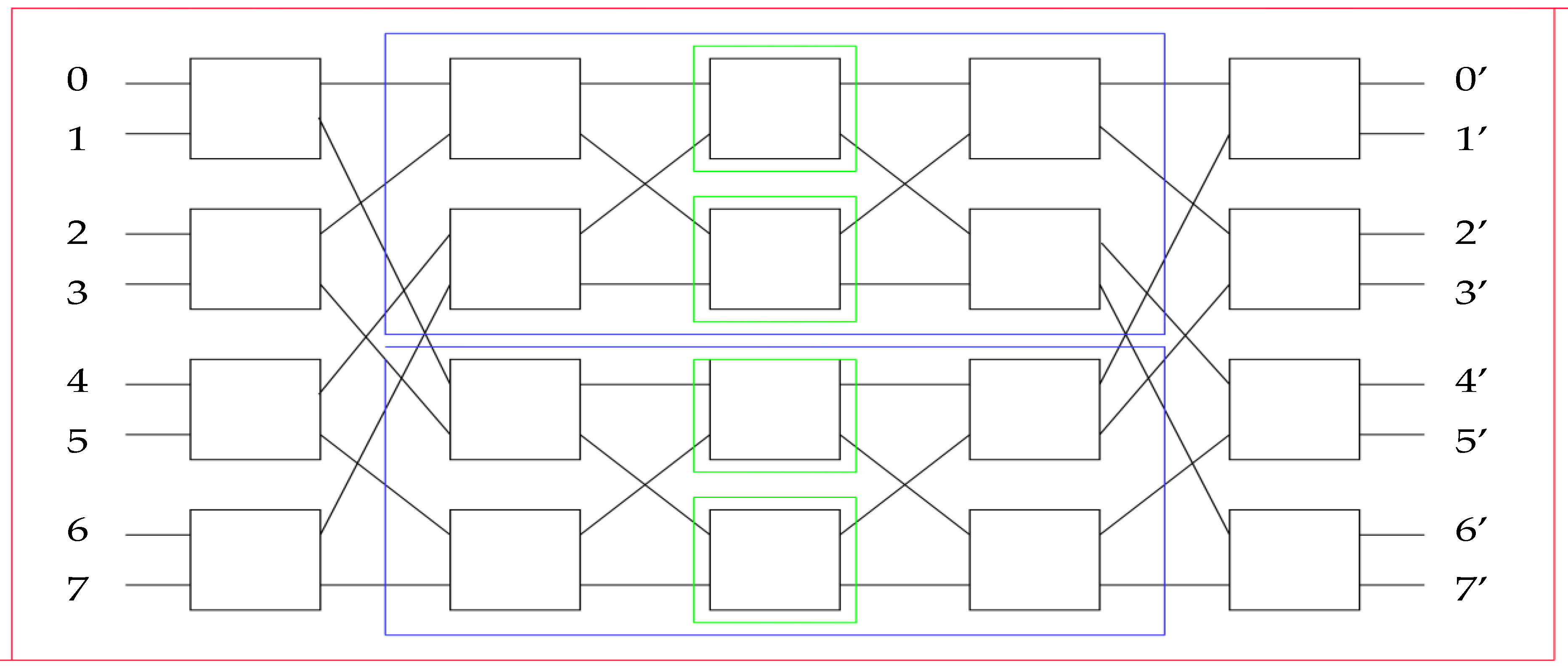
Proposition 1. The general recursive form of a Benes network is shown in
Figure 1. It has n = 2
r, r > 1, inputs, and n = 2
r outputs. All n ports (0, 1, 2, 3) are the input ports and all n’ ports (0′, 1′, 2′, 3′) are the output ports. There are m = 2
r – 1 input switches and m’ = 2
r – 1’ output switches. There are 2 subnetworks in the center, upper (U) and lower (L). These 2 subnetworks are Benes networks with 2
r−1 inputs and 2
r−1 outputs (half of the original network).
Proposition 2. In a Benes network with 2
r inputs and outputs, there are r layers. r − 1 layers with 2
r switches (input and output switches) and 1 layer (the center layer) with 2
r−1 switches. Layer k ∈ [0, r − 1], k has 2
k subnetworks with 2
(r-k) inputs, outputs each. The number of subnetworks doubles in each layer, while the number of inputs per subnetwork is halved.
Figure 2 presents an 8 input-output Benes network. As we can see, it is a Benes network of 2
3 = 8 (r = 3) input–output ports. Red is layer 0 (k = 0, 2
3 − 0 = 8 input–output ports per subnetwork, 2
0 = 1 subnetwork which is the original), blue is layer 1 (k = 1, 2
(3−1) = 4 input–output ports per subnetwork, 2
1 = 2 subnetworks), and green is layer 2 (k = 2, 2
(3−2) = 2 input–output ports per subnetwork, 4 switches/subnetworks). One layer has multiple subnetworks. With every layer, the number of subnetworks is doubled and number of inputs per subnetwork is halved. For this reason, the number of input and output switches of each layer remains the same, except in the last layer. Layer k = r − 1 is the center of the network and consists only of switches and not subnetworks (switches and subnetworks coincide).
Proposition 3. A switch (input or output) z ∈ [0, m − 1] (Proposition 1) has 2 input ports, 2 × z, and 2 × z + 1 and 2 output ports, 2 × z’ and 2 × z + 1′. For every switch, 2 settings are possible (
Figure 3). When 2 × z is connected to 2 × z + 1′ and 2 × z + 1 is connected to 2 × z’ the setting is cross. When 2 × z is connected to 2 × z’ and 2 × z + 1 is connected to 2 × z + 1′ the setting is bar. Satisfying the requested routing paths by setting all switches in the correct setting is the purpose of the routing algorithm.
Proposition 4. Because of the general form of the network (Proposition 1) and since 2 × z and 2 × z + 1 are ports of the same switch, they are connected to different subnetworks (up and down) regardless of the setting the switch has (cross or bar).
Proposition 5. If the switch is bar, input 2 × z is connected to the upper subnetwork and 2 × z + 1 is connected to the lower subnetwork; if the switch is cross, the opposite is true. The same stands for the outputs.
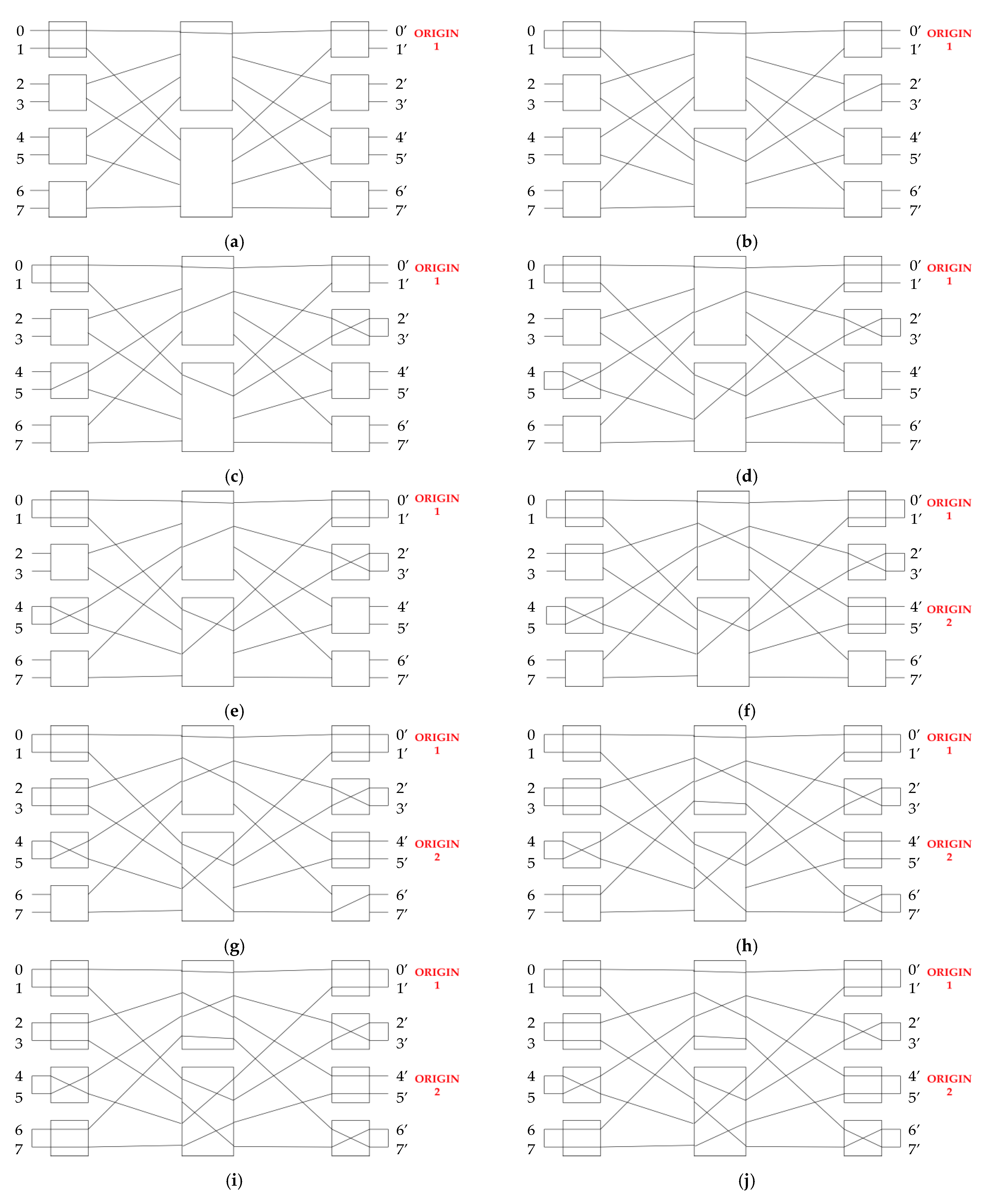
Proposition 6. If the subnetwork, with which every input and output is connected, is known, then by merit of Proposition 5, all switches can be configured correctly. Additionally, it is clear that the knowledge of the input–output table of the 2 subnetworks of the subsequent layer can be used to configure them. Therefore, the sequence that successfully routes layer 0 (the outmost layer) can be recursively used to route the inner layers and eventually the entire Benes network. This is related to the general form of the Benes network. The middle networks (the ones presented as “black boxes”) follow the exact same form as layer 0 (the outermost layer). The only thing required to route the outer layer is the input–output routing table. The process of routing the outer layer itself produces the input–output routing tables of the inner networks. This is shown in
Figure 4j clearly, where the lines connecting inputs–outputs of the inner networks can be seen. Each of these networks plays the same role for its own subnetworks and propagates the new routing tables. This process continues until all layers are routed fully.
4. Implementation
This section covers the hardware implementation of the algorithm described in the previous sections. The input of the circuit is the input–output routing table, and the output is the switches’ setting. After the routing is complete, it is expected that every output can be reached through its corresponding input.
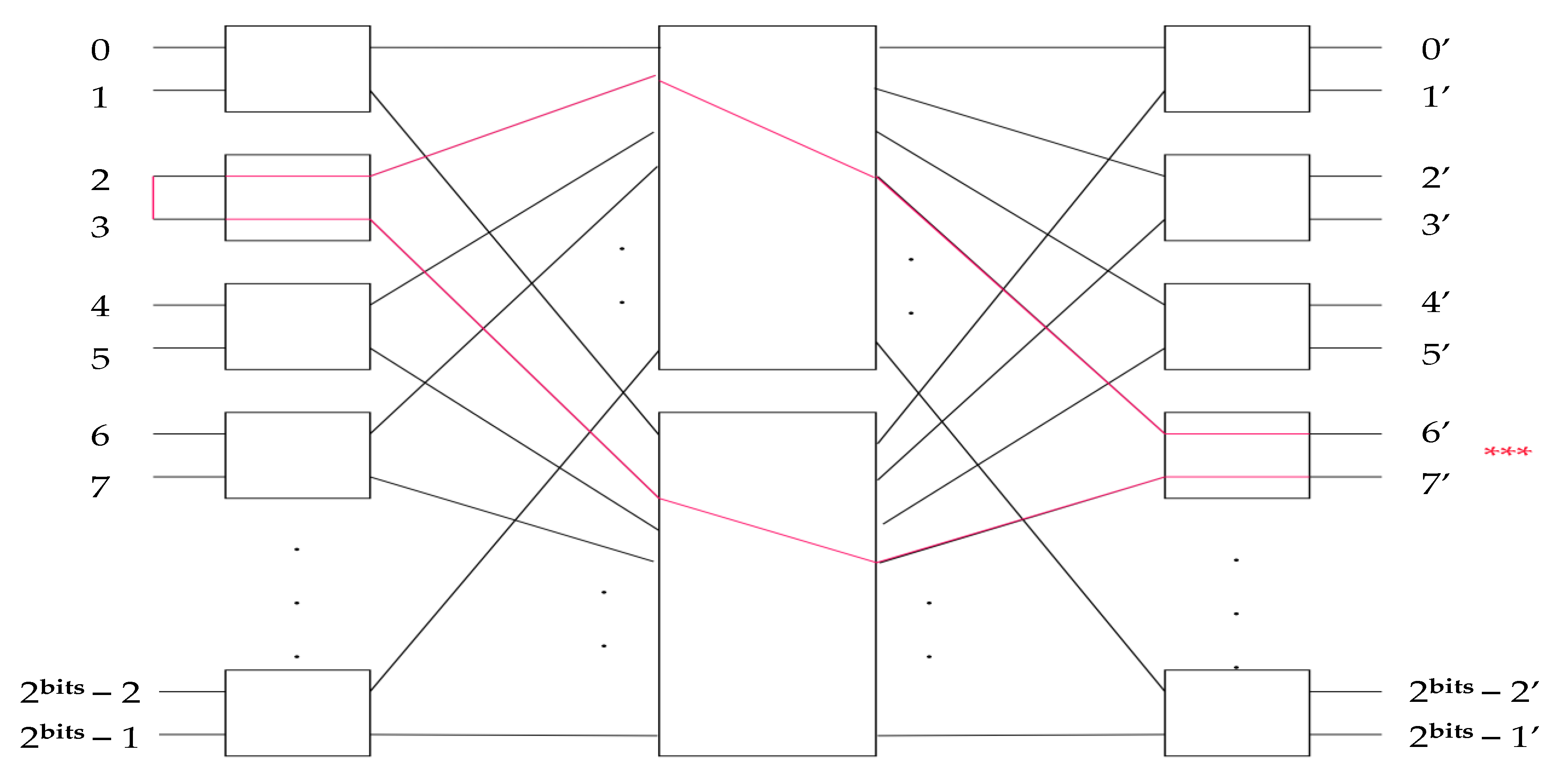
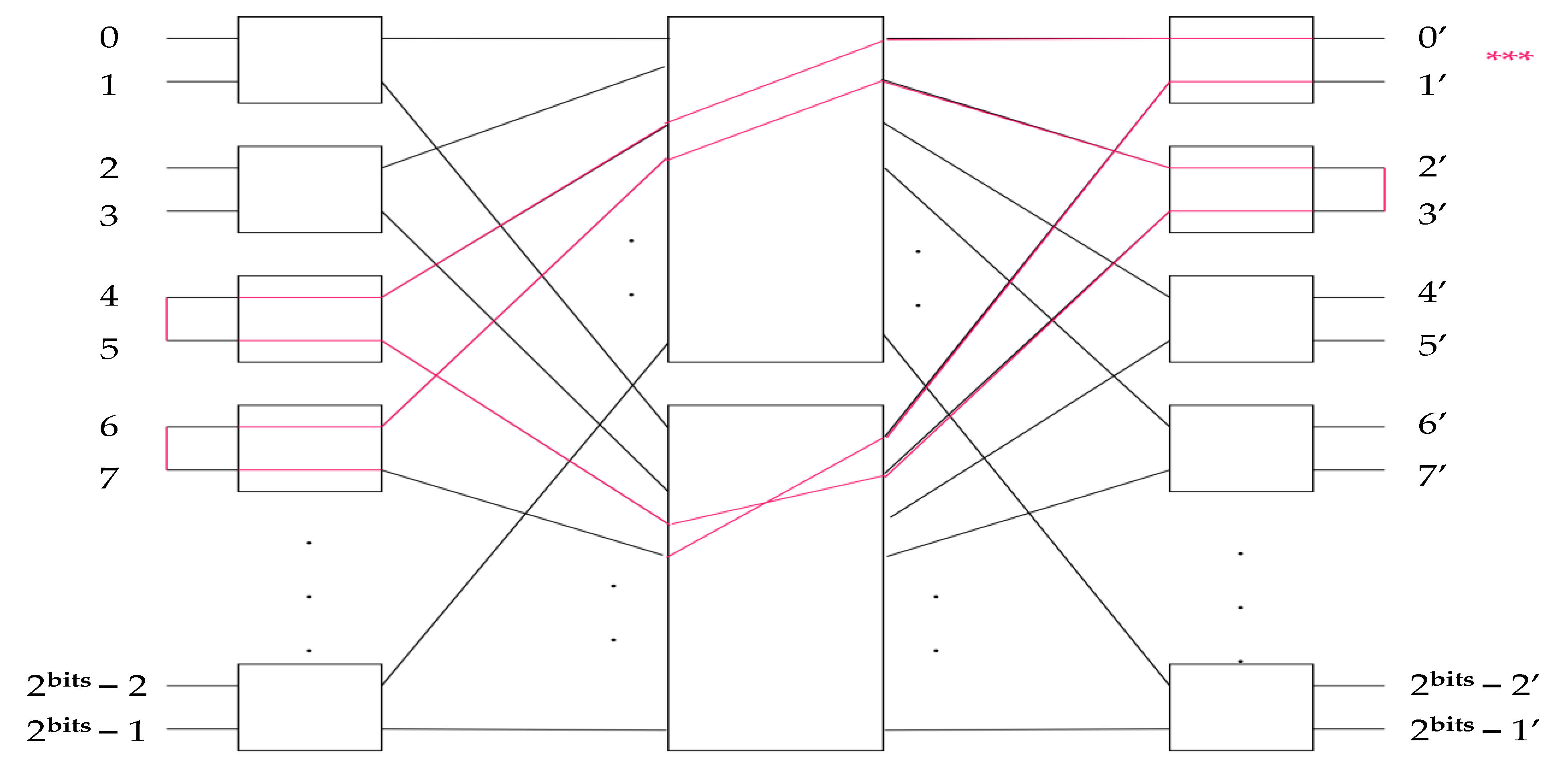
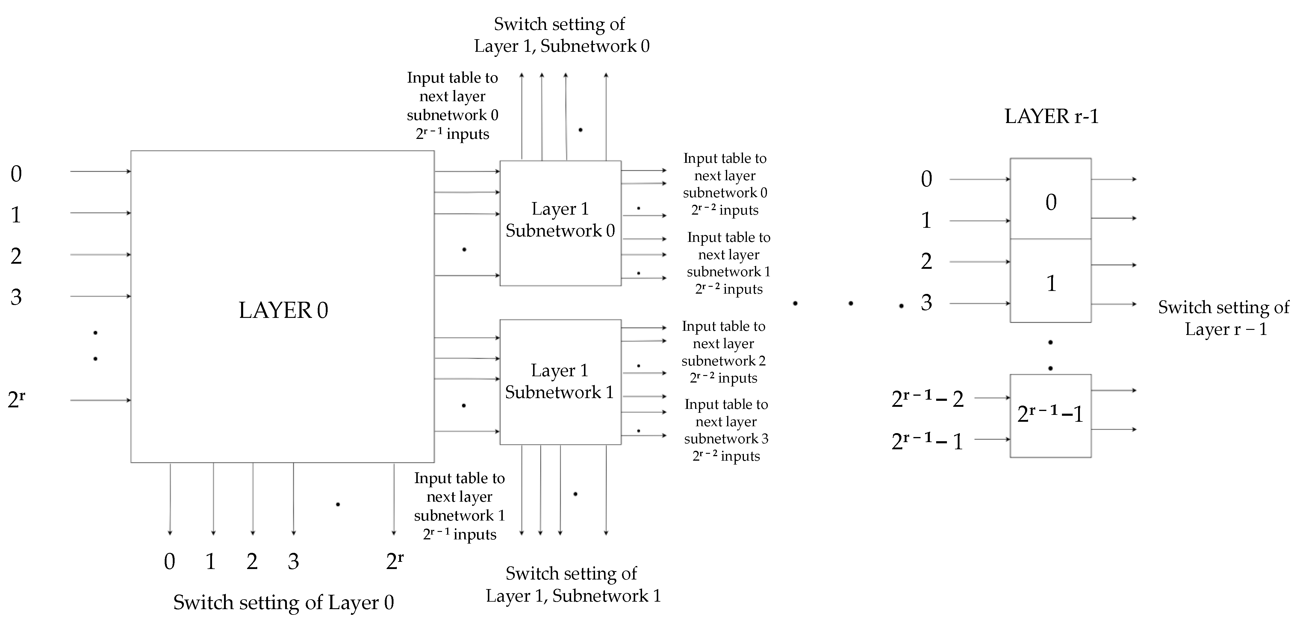
The recursive nature allows the use of the same circuit for every subnetwork albeit with a different number of inputs–outputs. The overall architecture of the design for a generic number of inputs is shown in
Figure 8. All subnetworks work identically. In each layer, the number of subnetworks is doubled, and the number of inputs per subnetwork is halved. The main output of each layer is the switches setting. The number of switches is the number of inputs–outputs (half input switches and half output switches) and is the same (2
r switches) for every layer, except the center (2
r−1 switches). Apart from the switches’ setting, each subnetwork also creates the input–output tables that it feeds to the next two subnetworks that replace it. In each instance, the act of “routing” inputs and outputs is translated to a simple sorting of the input–output entries. This sorting ensures that in the new list, pairs in 2 × z positions are routed through the upper subnetwork and pairs in 2 × z + 1 positions are routed through the lower subnetwork.
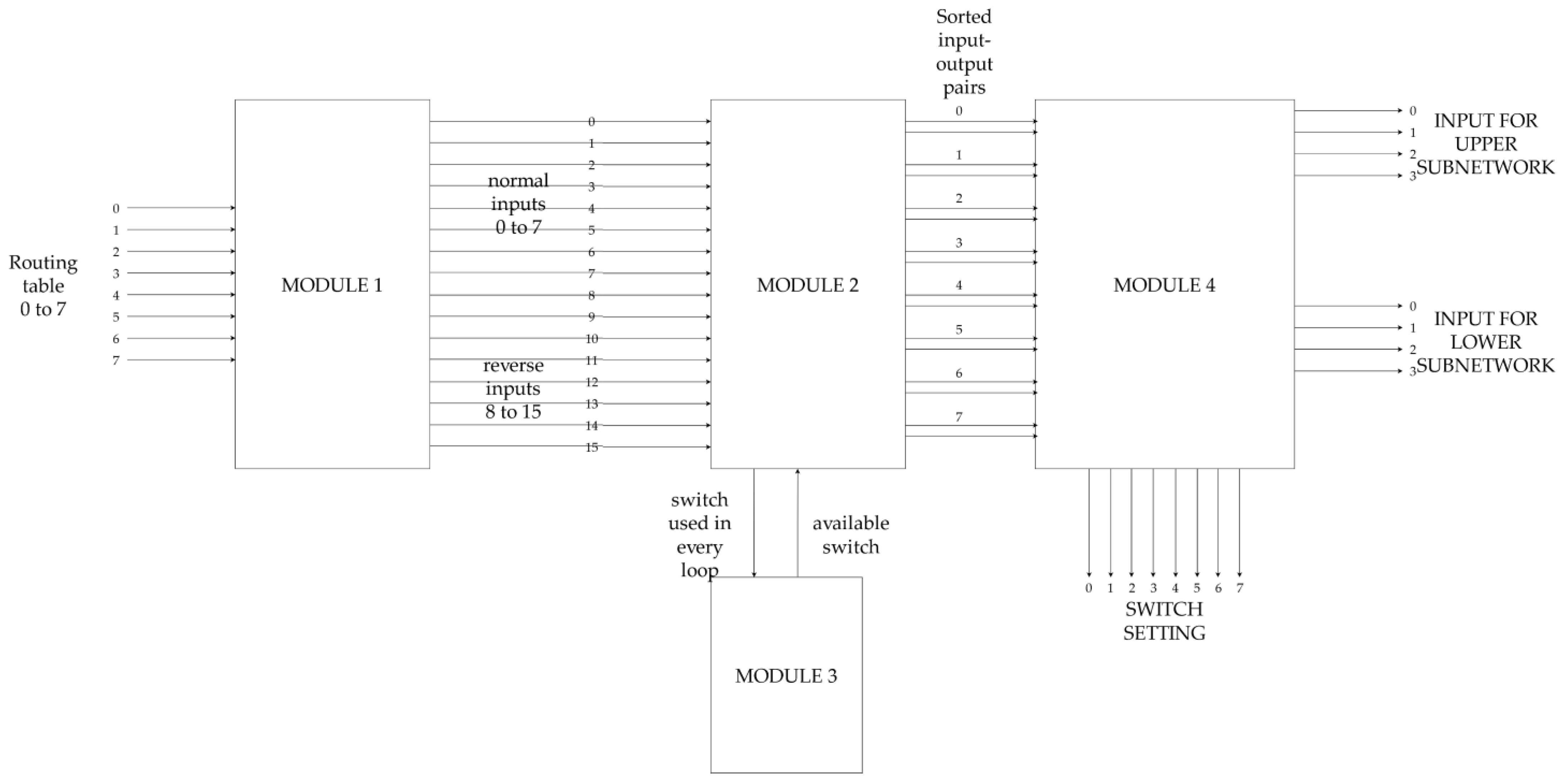
Figure 8 presents the subnetwork of the first layer with 2
r inputs. There are four modules. Modules 1 and 4 handle the input and output formatting, respectively. Modules 2 and 3 constitute the main system, and it is where the sorting takes place.
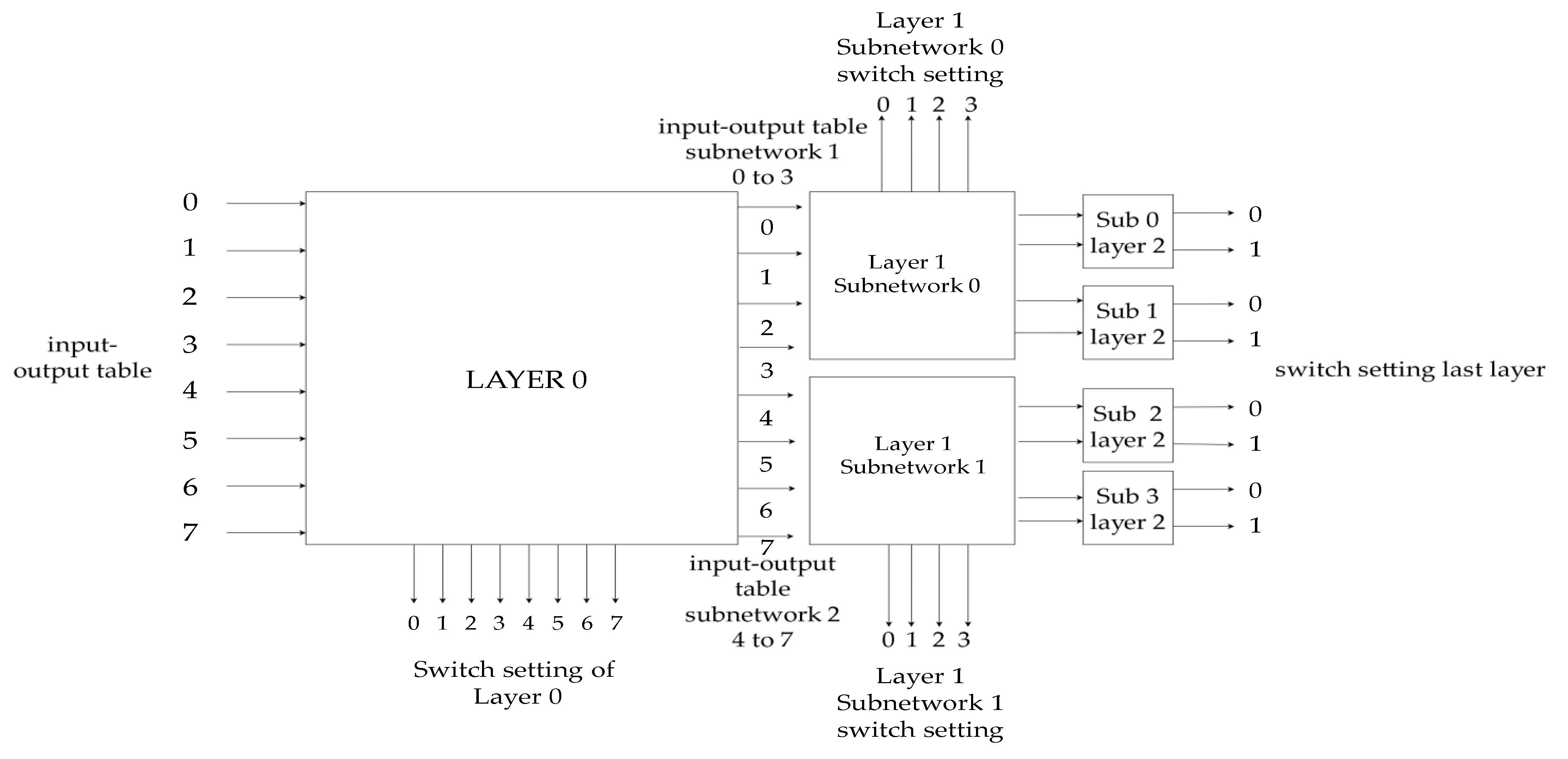
For the more detailed explanation of the system, we used an example of an 8 input–output network (
Figure 9). Out of all the subnetworks (Proposition 2) in the network, we focus on the function of the first layer (
Figure 10) (8 input–output ports, 8 switches). Proposition 6 ensures that once the first layer is routed, all others follow in the same way.
The choice to present things in this way was primarily made in order to present the concept of each module in a concise way, which is easy to follow. The relationship between the 8-port network and the generic version is examined in each module section separately.
4.1. Module 1: Reverse Input Vector
This module creates the inverse input vector of the input–output routing table. The process uses the number of the output as the index of the inverse vector entries. For example,
Table 2 presents the input–output routing table of an 8-port Benes network.
Input port 0 leads to output port 0′. Input port 1 leads to output port 2′. Port 2 to 4′, etc. The inverse vector contains the output ports on the left side in an ascending order and their respective input port on the right side. In our example, position 2′ in the new vector is filled with the number 1, position 0′ with the number 0, and 4′ with 2. The entire reverse vector in shown in
Table 3.
The left side of both vectors are always in an ascending order. That is why we can simply keep the right side and use the index of the input vectors as the left side. The right side of these two vectors is the input that is fed to the first layer and starts the entire routing process.
In the case of a generic number of input ports, nothing changes. We use the left side as an index and complete the inverse vector. If there is more than one zero elements, two or more input ports are connected to the same output. With n = 2r inputs, the creation of the inverse vector needs 1 clock cycle. The creation of the inverse vector is necessary in order to be able to find the corresponding port to an input or an output without searching the entire vector.
4.2. Module 2: Sorting Mechanism
Module 2 implements the algorithm described in the
Section 3. In every cycle, it routes two paths: one from the outputs to the inputs and one from the inputs back to the outputs. In the circuit environment, “routing” means sorting input–output pairs in a way in which pairs in 2 × m positions are routed through the upper network and pairs in 2 × m + 1 positions are routed through the lower network. Whether it is up and down, or down and up, makes no difference to the solution. Utilizing the two indexed vectors (
Table 2 and
Table 3), a detailed run of the algorithm is shown below. As we mentioned in
Section 3, one iteration consists of all steps, essentially routing an output to an input and routing the input of the same switch back to the output.
1st iteration. Any output can be selected to start the algorithm, but in our case, we select output 0′ as the origin point of the first path (
Table 4).
2nd iteration. The output for the next iteration is 3′ since it in the same switch as 2′ (
Table 5). This is detected simply by dividing the number of the 2 ports by 2.
3rd iteration. 1′ is in the same switch as 0′ so a new path must be created. Output port 4′ is the new origin point (
Table 6).
4th iteration. 7′ is in the same switch as 6′. Last iteration since all switches are routed (
Table 7). This is the same example that is presented in
Figure 4.
In the case of a generic number of inputs, the algorithm is the same. We keep repeating the same steps until all switches are routed. The process is linear, and, in every clock cycle, two switches are routed. For 2r = n input, 2r−1 = n/2 clock cycles are needed.
4.3. Module 3: Unrouted Switch Pointer
Module 3 is a complementary module to the previous part. It is responsible for selecting the next starting point (origin) in the case of a path loop. For example, in iteration 2 (
Table 5), the path ends in a loop on output switch 0′ (output ports 0′,1′). To continue the process, a new starting point is necessary. When there are no more available switches in Module 3, all loops are closed, and the algorithm ends. In order to avoid the long critical path of the priority encoder needed for the 1st implementation, a different design is considered. Every switch element, with the use of two auxiliary vectors, becomes a part of a linked list. Vector (left) contains the list entries on the left of each element and vector (right) contains the list entries on the right of each element. The head of the list is the first available pair. When an element is used in Module 2, it is ejected from the list by connecting the two adjacent entries. If the head is selected, then it is ejected, and the head pointer moves to the left entry. The list is always organized from left to right. An equivalent run to the first implementation is as follows.
1st iteration. The two vectors (left) and (right) have four entries, one for every output switch. The initial values for these entries are the adjacent switches. For example, position 1 refers to the 1′ switch (ports 2′,3′). Left of 1 is 2, and therefore, left [
1] = 2; right of 2 is 3, and therefore right [
1] = 3. Switch 0′ (ports 0′,1′) does not contribute since it is always routed first. The other vector cells are initialized with the same logic (
Table 8). The head of the list is switch 1′ (ports 2′,3′), head = 1′.
2nd iteration. Output switch 1′ is ejected from the list. Switch 2′ (4′,5′) becomes head of the list, head = 2′ (
Table 9).
3rd iteration. A path loop is reached. Output switch 2′ (head of list) is used to proceed with the routing. Consequently, switch 2′ is ejected from the list (
Table 10).
4th iteration. Output switch 3′ is ejected from the list. The routing is complete (
Table 11).
Such an implementation dramatically improves the speed of the circuit. It allows us to avoid using logical constructs with long critical paths, such as a priority encoder to decide the availability of switches.
4.4. Module 4: Switch Routing and Input-Output Routing Tables of the Next Layer
The last module of the design reads the sorted list of pairs and routes the input and output switches accordingly. It reads every two entries in each side since adjacent entries belong to the same switch. In the case of a path loop, since the path has 2 × k + 1 steps, it never samples the same switch. If a 2 × m input or output is the first input/output of a switch, then the switch is bar. If it is the second one, then the switch is cross. It also prepares the input–output table for the two subnetworks. The process is completed in n/2 cycles.
After sorting the entries with the previous modules, we now have the mapping of the paths (
Table 12). All pairs in 2 × m positions are routed through the upper Benes subnetwork, and all pairs in 2 × m + 1 are routed through the lower subnetwork. We check all 2 × m positions of the table and determine the routing of both input and output switches. In position 0, there is input port 0 and output port 0′. Both ports 0 and 0′ are the first port of their respective switch, so both switches are routed bar according to Proposition 5 (
Table 13).
The next 2 × m position is position 2 (3rd row). The respective ports are 5 and 3′. Both are the second port of their respective switch, so both switches are cross (switch 2 for 5 and switch 1′ for 3′) (
Table 14).
Position 4 (5th row) contains ports 2 and 4′. They are both the first port of their respective switch, so both switches are set to bar (
Table 15).
Position 6 (7th row) contains ports 6 and 7′. Here, port 6 is the first input of input switch 3 and 7′ is the second output of switch 3′. Switch 3 is set to bar, and switch 3′ is set to cross (
Table 16).
The entire layer is presented routed in the picture below (
Figure 11).
Regarding the input routing tables to the next layers (upper and lower subnetworks), each switch can only be connected to a subnetwork once. The number of a subnetwork port that a switch is connected to is the same as the number of the switch (Proposition 2). For this reason, in order to produce the input–output tables for the next layer, we separate the input–output pairs (
Table 12) by their subnetwork (
Table 17 and
Table 18).
We then must divide by 2. This division is necessary in order to produce a valid routing table since subnetworks have half the number of input and output ports (
Table 19 and
Table 20).
Finally, the pairs are organized in the same manner (ascending input order) as the original input–output routing table (
Table 21 and
Table 22).
At this point, the tables are passed as inputs to the subnetworks of the next layer and are used to route it (Proposition 6). The process repeats until all switches on all layers are set. The entire fully routed network can be seen in
Figure 12.
The process is linear in this case also, and it is the same for a generic number of inputs, as nothing changes. We simply keep setting the switches until the end. Since we use only 2 × m positions for 2r inputs, 2r-1 = n/2 clock cycles are needed.
The cycles of the individual modules are Module 1: 1, Module 2:
n/2, Module 3: 1, Module 4:
n/2, and thus, 1 +
n/2 + 1 +
n/2 = 2 +
nn total cycles. Due to the recursiveness of the Benes network (Proposition 1) there are log
n = r layers of subnetworks. The complexity of the entire system is log
n ×
n, the minimum complexity to route a Benes network with one processing unit [
23].
5. Board Implementation, Results and Discussion
In [
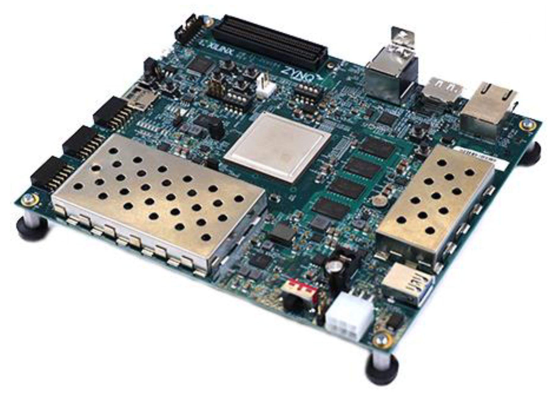
32], the author used the Taiwan Semiconductor Manufacturing Company (TSMC) ASIC libraries to implement their work. In our case, we implemented the design on the mid-range FPGA board, ZCU-104 Evaluation board (
Figure 13) using Vivado. In order to leave as many resources as possible available for the algorithm to utilize, we used a single pin for the input and a single pin for the output.
The input–output routing table entries were linearly inserted to a shift register (input vector), whose elements became the corresponding output port (
Table 23). In the example, port 0 is paired with port 0′. So, the first 3 bits are 000. Port 1 is paired with port 2′, so the next 3 bits are 010. Using this logic, the corresponding input vector of the example is 000 010 100 110 001 011 111 101. For a generic size of 2
r inputs, the input vector’s size is r × 2
r bits.
The same logic applies to the output. For all layers, the setting of all switches is loaded to a shift register connected to the single output pin. The size of the output shift register for a Benes network of 2
r inputs is (r − 1) × 2
r + 2
r−1 bits. Each switch is represented by one bit: 1 for cross setting and 0 for bar setting (Proposition 3). There are (r − 1) layers with 2
r switches and one layer with 2
r−1 switches (Proposition 2).
Table 24 shows the output vector of the 8 × 8 example per layer (Proposition 2). The first 4 bits are the input switches of the first layer (red). The next 4 are the output switches of the first layer, etc.
The design was implemented originally for Benes networks of size 8, 16, 32, and 64 (
Table 25).
The operational frequency along with the time needed to produce one fully routed setting is listed below (
Table 26). Complexity of the algorithm is
n × log
n so in order to find the time need to produce one complete result, we multiply the required clock cycles with the minimum period (
Table 26). No DSP, RAM blocks or other specialized blocks were used.
Lastly, we have the power consumed as reported by the Vivado tool (
Table 27).
In [
32], the author provides a utilization report on a synthesized ASIC implementation of Lee’s algorithm [
28]. For a 64-port network, the parallel design consumes around 1.32 × 10
5 logic cells and needs 5.6 × 36 = 201.6 ns (5.6 ns being the critical path and 36 the needed clock cycles to complete 1 operation) to complete one routing.
A rather rough comparison between these two implementation approaches could be done as follows. According to [
33], the fact that architectures built on FPGAs are, on average, 35 times larger and 4 times slower than those build on ASICs, these values can be converted to FPGA terms. However, the difference in the technology nodes (65 nm vs. 16 nm of the used FPGA) should be taken into account since there is a proportional increase in devices speed, according to the scaling factor. More specifically, the above correspond to an area of 132,000 × 35 = 4,620,000 cells and a required time of 201.6 × 4/4 = 201.6 ns. By merit of this analogy, it seems that the metric of space × time is lower in our design (49,466 × 3072 < 4,620,000 × 201.6) by a factor of 6.12.
Apart from parallel and linear routing algorithms, there is another approach to routing interconnection networks and networks in general. Machine learning has risen to prominence in recent years and is being used in many different areas of networking, including network routing. In our case, machine learning-assisted routing of Benes networks primarily concerns photonic switches. Researchers have opted to used machine learning for Benes switch routing since it is less resource demanding compared to the already established algorithms. The author of [
34] conducted extensive work on the subject. In [
34], a photonic 4 × 4 Benes switch was routed using machine learning techniques. The author stated that there are 2
6 = 64 possible combinations. This is drastically more than our model which needs only 4 × log24 = 4 × 2 = 8 clock cycles (
n × log2
n,
n = 4) to complete the routing. In [
35], the same trend is continuous. For a classic 8 × 8 Benes network, the possible combinations are in the range of millions. This would require much more time than our approach of 8log28 = 8 × 3 = 24 clock cycles/steps. The author also used non-classic, arbitrary size Benes networks [
36] with ports not equal to a power of 2. The modification needed for our proposed algorithm to route all kinds of Benes networks (arbitrary size and classic) will be the subject of our future work. It seems that the proposed algorithm can replace both hard and soft existing computing methods. It is straightforward enough to be implemented easily and does not consume a lot of resources. As it was presented, parallel solutions require too many resources while not offering the counterweight advantages in terms of speed (metric speed × space) and machine learning has to contend with very big data sets (millions for 8 × 8 Benes switch).

